Archive for August, 2014
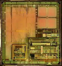
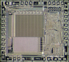
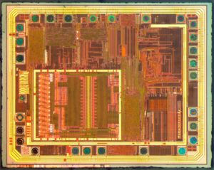
 Recover IC PIC16F687 Software

Recover IC PIC16F687 Software
The Program Counter (PC) is 13 bits wide. The low byte comes from the PCL register, which is a recoverable and writable register which can be used for Recover IC PIC16F687 Software. The high byte (PC<12:8>) is not directly recoverable or writable and comes from PCLATH. On any Reset, the PC is cleared. Figure 2-9 shows the two situations for the loading of the PC. The upper example in Figure 2-9 shows how the PC is loaded on a write to PCL (PCLATH<4:0> → PCH). The lower example in Figure 2-9 shows how the PC is loaded during aCALL or GOTO instruction (PCLATH<4:3> → PCH).
The PIC16F687 devices have an 8-level x 13-bit wide hardware stack. The stack space is not part of either program or data space and the Stack Pointer is not recoverable or writable. The PC is PUSHed onto the stack when a CALL instruction is executed or an interrupt causes a branch. The stack is POPed in the event of a RETURN, RETLW or a RETFIE instruction execution. PCLATH is not affected by a PUSH or POP operation.
The stack operates as a circular buffer. This means that after the stack has been PUSHed eight times, the ninth push overwrites the value that was stored from the first push. The tenth push overwrites the second push (and so on).
Executing any instruction with the PCL register as the destination simultaneously causes the Program Counter PC<12:8> bits (PCH) to be replaced by the contents of the PCLATH register. This allows the entire contents of the program counter to be changed by writing the desired upper 5 bits to the PCLATH register.
When the lower 8 bits are written to the PCL register, all 13 bits of the program counter will change to the values contained in the PCLATH register and those being written to the PCL register after Recover IC PIC16F687 Software.
Circuit Engineering Company Limited continues to be recognized as the Southern China Leader in Services for IC recovering. With the advancement of today’s modern circuit board technology, it is more important than ever to have specialists available to help you at a moment’s notice. Our engineering and commercial teams collectively have a vast amount of electronic experience covering field include Consumer Electronics, Industrial Automation Electronics, Wireless Communication Electronics., etc. For more information please contact us through email.
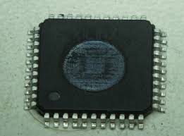
Break Microcontroller PIC16F690 Heximal
Break Microcontroller PIC16F690 Heximal
We can Break Microcontroller PIC16F690 Heximal, please view the Microcontroller PIC16F684 features for your reference:
High-Performance RISC CPU:
· Only 35 instructions to learn:
– All single-cycle instructions except branches
· Operating speed:
– DC – 20 MHz oscillator/clock input
– DC – 200 ns instruction cycle
· Interrupt capability
· 8-level deep hardware stack
Low-Power Features:
· Standby Current:
– 1 nA @ 2.0V, typical
· Operating Current:
– 8.5 µA @ 32 kHz, 2.0V, typical
– 100 µA @ 1 MHz, 2.0V, typical
· Watchdog Timer Current:
– 1 µA @ 2.0V, typical
· Direct, Indirect and Relative Addressing modes
Peripheral Features:
Special Microcontroller Features:
· Precision Internal Oscillator:
– Factory calibrated to ±1%
– Software selectable frequency range of 8 MHz to 31 kHz
– Software tunable
– Two-speed Start-up mode
– Crystal fail detect for critical applications
– Clock mode switching during operation for power savings
· Power-saving Sleep mode
· Wide operating voltage range (2.0V-5.5V)
· Industrial and Extended Temperature range
· Power-on Reset (POR)
· Power-up Timer (PWRT) and Oscillator Start-up Timer (OST)
· Brown-out Detect (BOD) with software control option
· Enhanced low-current Watchdog Timer (WDT) with on-chip oscillator (software selectable nominal 268 seconds with full prescaler) with software enable to facilitate the process of Break Microcontroller PIC16F690 Heximal.
· Multiplexed Master Clear with pull-up/input pin
· Programmable code protection
· High Endurance Flash/EEPROM cell:
– 100,000 write Flash endurance
– 1,000,000 write EEPROM endurance
– Flash/Data EEPROM retention: > 40 years
· 12 I/O pins with individual direction control:
– High current source/sink for direct LED drive
– Individually programmable weak pull-ups
– Ultra Low-power Wake-up (ULPWU)
· Analog comparator module with:
– Two analog comparators
– Programmable on-chip voltage reference (CVREF) module (% of VDD)
– Comparator inputs and outputs externally accessible
· A/D Converter:
– 10-bit resolution and 8 channels
· Timer0: 8-bit timer/counter with 8-bit programmable prescaler
· Enhanced Timer1:
– 16-bit timer/counter with prescaler
– External Gate Input mode
– Option to use OSC1 and OSC2 in LP mode as Timer1 oscillator if INTOSC mode selected
· Timer2: 8-bit timer/counter with 8-bit period register, prescaler and postscaler
· Enhanced Capture, Compare, PWM module:
– 16-bit Capture, max resolution 12.5 ns
– Compare, max resolution 200 ns
– 10-bit PWM with 1, 2 or 4 output channels, programmable “dead time”, max frequency 20 kHz
· In-Circuit Serial ProgrammingTM (ICSPTM) via two pins
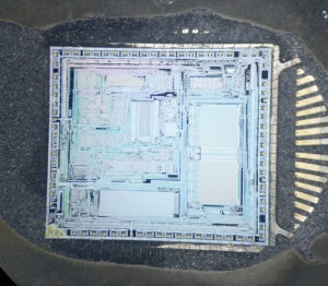
Recover IC PIC16F72A Binary
Recover IC PIC16F72A Binary
This document contains device-specific information for Recover IC PIC16F72A Binary. Additional information may be found in the PICmicro™ Mid-Range Reference Manual, (DS33023), which may be obtained from your local Microchip Sales Representative or downloaded from the Microchip website.
The Reference Manual should be considered a complementary document to this data sheet, and is highly recommended reading for a better understanding of the device architecture and operation of the peripheral modules. There are two devices (PIC16C72A) covered by this datasheet. The PIC16C72A does not have the A/D module implemented.
The Special Function Registers are registers used by the CPU and Peripheral Modules for controlling the desired operation of the device. These registers are implemented as static RAM.
The STATUS register, shown in Register 2-1, contains the arithmetic status of the ALU, the RESET status and the bank select bits for data memory.
The STATUS register can be the destination for any instruction, as with any other register. If the STATUS register is the destination for an instruction that affects the Z, DC or C bits, the write to these three bits is disabled after Recover IC PIC16F72A Binary.
These bits are set or cleared according to the device logic. The TO and PD bits are not writable. The result of an instruction with the STATUS register as destination may be different than intended.
For example, CLRF STATUS will clear the upper-three bits and set the Z bit. This leaves the STATUS register as 000u u1uu (where u = unchanged).
Circuit Engineering Company Limited continues to be recognized as the Southern China Leader in Services for IC Read, MCU Recover, Chip Extract, Microcontroller Unlock service. With the advancement of today’s modern circuit board technology, it is more important than ever to have specialists available to help you at a moment’s notice.
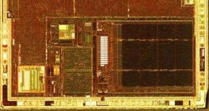
Break Microcontroller PIC16C65B Eeprom
The PIC16C65B devices are low cost, high performance, CMOS, fully-static, 8-bit microcontrollers in the PIC16CXX mid-range family. All PICmicro® microcontrollers employ an advanced RISC architecture which has been fully researched and becoming easier to Break Microcontroller PIC16C65B Eeprom.
The PIC16CXX microcontroller family has enhanced core features, eight-level deep stack and multiple internal and external interrupt sources.
The separate instruction and data buses of the Harvard architecture allow a 14-bit wide instruction word with the separate 8-bit wide data. The two stage instruction pipeline allows all instructions to execute in a single cycle, except for program branches, which require two cycles, A total of 35 instructions (reduced instruction set) are available. Additionally, a large register set gives some of the architectural innovations used to achieve a very high performance.
The PIC16C63A/73B devices have 22 I/O pins. The PIC16C65B/74B devices have 33 I/O pins. Each device has 192 bytes of RAM. In addition, several peripheral features are available, including: three timer/ counters, two Capture/Compare/PWM modules, and two serial ports;
The Synchronous Serial Port (SSP) can be configured as either a 3-wire Serial Peripheral Interface (SPI) or the two-wire Inter-Integrated Circuit (I 2C) bus. The Universal Synchronous Asynchronous Receiver Transmitter (USART) is also known as the Serial Communications Interface or SCI. Also, a 5- channel high speed 8-bit A/D is provided while the PIC16C74B offers 8 channels.
The 8-bit resolution is ideally suited for applications requiring low cost analog interface, e.g., thermostat control, pressure sensing, etc. The PIC16C65B devices have special features to reduce external components, thus reducing cost, enhancing system reliability and reducing power consumption which makes engineer more likely to choose it as the next generation of device and necessary to Break Microcontroller PIC16C65B Eeprom.
There are four oscillator options, of which the single pin RC oscillator provides a low cost solution, the LP oscillator minimizes power consumption, XT is a standard crystal, and the HS is for high speed crystals. The SLEEP (power-down) feature provides a power-saving mode. The user can wake-up the chip from SLEEP through several external and internal interrupts and RESETS.
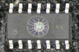
Attack MCU PIC16C715 Software
Attack MCU PIC16C715 Software
PORTB is an 8-bit wide bi-directional port. The corresponding data direction register is TRISB. Setting a bit in the TRISB register puts the corresponding output driver in a hi-impedance input mode when Attack MCU PIC16C715 Software. Clearing a bit in the TRISB register puts the contents of the output latch on the selected pin(s).
Each of the PORTB pins has a weak internal pull-up. A single control bit can turn on all the pull-ups. This is performed by clearing bit RBPU (OPTION<7>). The weak pull-up is automatically turned off when the port pin is configured as an output. The pull-ups are disabled on a Power-on Reset.
Four of PORTB’s pins, RB7:RB4, have an interrupt on change feature. Only pins configured as inputs can cause this interrupt to occur (i.e. any RB7:RB4 pin configured as an output is excluded from the interrupt on change comparison).
The input pins (of RB7:RB4) are compared with the old value latched on the last attack of PORTB. The “mismatch” outputs of RB7:RB4 are OR’ed together to generate the RB Port Change Interrupt with flag bit RBIF (INTCON<0>).
Any instruction which writes, operates internally as a attack followed by a write operation. The BCF and BSF instructions, for example, attack the register into the CPU, execute the bit operation and write the result back to the register to ease the process of Attack MCU PIC16C715 Software. Caution must be used when these instructions are applied to a port with both inputs and outputs defined.
For example, a BSF operation on bit5 of PORTB will cause all eight bits of PORTB to be attack into the CPU. Then the BSF operation takes place on bit5 and PORTB is written to the output latches.
If another bit of PORTB is used as a bi-directional I/O pin (e.g., bit0) and it is defined as an input at this time, the input signal present on the pin itself would be attack into the CPU and rewritten to the data latch of this particular pin, overwriting the previous content. As long as the pin stays in the input mode, no problem occurs. However, if bit0 is switched to an output, the content of the data latch may now be unknown.
The actual write to an I/O port happens at the end of an instruction cycle, whereas for attacking, the data must be valid at the beginning of the instruction cycle. Therefore, care must be exercised if a write followed by a attack operation is carried out on the same I/O port. The sequence of instructions should be such to allow the pin voltage to stabilize (load dependent) before the next instruction which causes that file to be attack into the CPU is executed.
Otherwise, the previous state of that pin may be attack into the CPU rather than the new state. When in doubt, it is better to separate these instructions with a NOP or another instruction not accessing this I/O port.
Recover Chip PIC18F1330 Code
Memory Endurance: The Enhanced Flash cells for both program memory and data EEPROM are rated to last for many thousands of erase/write cycles – up to 100,000 for program memory and 1,000,000 for EEPROM. Data retention without refresh is conservatively estimated to be greater than 40 years.
Self-Programmability: These devices can write to their own program memory spaces under internal software control. By using a boot loader routine located in the protected Boot Block at the top of program memory, it becomes possible to create an application that can update itself in the field.
· Extended Instruction Set: The PIC18F1230/1330 family introduces an optional extension to the PIC18 instruction set, which adds eight new instructions and an Indexed Addressing mode. This extension, enabled as a device configuration option, has been specifically designed to optimize re-entrant application code originally developed in high-level languages, such as C.
· Power Control PWM Module: This module provides up to six modulated outputs for controlling half-bridge and full-bridge drivers. Other features include auto-shutdown on Fault detection and auto-restart to reactivate outputs once the condition has cleared.
· Enhanced Addressable USART: This serial communication module is capable of standard RS-232 operation and provides support for the LIN bus protocol. Other enhancements include automatic baud rate detection and a 16-bit Baud Rate Generator for improved resolution from Recover Chip PIC18F1330 Code.
When the microcontroller is using the internal oscillator block, the EUSART provides stable operation for applications that talk to the outside world without using an external crystal (or its accompanying power requirement).
· 10-Bit A/D Converter: This module incorporates programmable acquisition time, allowing for a channel to be selected and a conversion to be initiated without waiting for a sampling period and thus, reducing code overhead can help to Recover Chip PIC18F1330 Code.
· Extended Watchdog Timer (WDT): This enhanced version incorporates a 16-bit prescaler, allowing an extended time-out range that is stable across operating voltage and temperature.
See Section 22.0 “Electrical Characteristics” for time-out periods. Devices in the PIC18F1230/1330 family are available in 18-pin, 20-pin and 28-pin packages. The devices are differentiated from each other in one way:
1. Flash program memory (4 Kbytes for PIC18F1230, 8 Kbytes for PIC18F1330). All other features for devices in this family are identical. Like all Microchip PIC18 devices, members of the PIC18F1230/1330 family are available as both standard and low-voltage devices.
Standard devices with Enhanced Flash memory, designated with an “F” in the part number (such as PIC18F1330), accommodate an operating VDD range of 4.2V to 5.5V. Low-voltage parts, designated by “LF” (such as PIC18LF1330), function over an extended VDD range of 2.0V to 5.5V.
Break Microcontroller PIC18F4220 Binary
· Self-programmability: These devices can write to their own program memory spaces under internal software control. By using a bootloader routine located in the protected Boot Block at the top of program memory to Break Microcontroller PIC18F4220 Binary, it becomes possible to create an application that can update itself in the field.
· Enhanced CCP Module: In PWM mode, this module provides 1, 2 or 4 modulated outputs for controlling half-bridge and full-bridge drivers. Other features include Auto-Shutdown for disabling PWM outputs on interrupt or other select conditions and Auto-Restart to reactivate outputs once the condition has cleared.
Addressable USART: This serial communication module is capable of standard RS-232 operation using the internal oscillator block, removing the need for an external crystal (and its accompanying power requirement) in applications that talk to the outside world.
· 10-bit A/D Converter: This module incorporates programmable acquisition time, allowing for a channel to be selected and a conversion to be initiated without waiting for a sampling period and thus, reduce code overhead.
· Extended Watchdog Timer (WDT): This enhanced version incorporates a 16-bit prescaler, allowing a time-out range from 4 ms to over 2 minutes, that is stable across operating voltage and temperature.
The EC and ECIO Oscillator modes require an external clock source to be connected to the OSC1 pin. There is no oscillator start-up time required after a Power-on Reset or after an exit from Sleep mode. In the EC Oscillator mode, the oscillator frequency divided by 4 is available on the OSC2 pin. This signal may be used for test purposes or to synchronize other logic by Break Microcontroller PIC18F4220 Binary.
For timing insensitive applications, the “RC” and “RCIO” device options offer additional cost savings. The RC oscillator frequency is a function of the supply voltage, the resistor (REXT) and capacitor (CEXT) values and the operating temperature.
In addition to this, the oscillator frequency will vary from unit to unit due to normal manufacturing variation. Furthermore, the difference in lead frame capacitance between package types will also affect the oscillation frequency, especially for low CEXT values.
The user also needs to take into account variation due to tolerance of external R and C components used. Figure 2-6 shows how the R/C combination is connected. In the RC Oscillator mode, the oscillator frequency divided by 4 is available on the OSC2 pin. This signal may be used for test purposes or to synchronize other logic.
Recover Microcontroller MSP430F4361 Flash
Recover Microcontroller MSP430F4361 Flash from Texas Instruments (TI) are 16-bit, RISC-based, mixed-signal processors designed specifically for ultra-low-power. MSP430 MCUs have the right mix of intelligent peripherals, ease-of-use, low cost and lowest power consumption for thousands of applications – including Recover Microcontroller MSP430F4361 Flash.
TI offers robust design support for the MSP430 MCU platform along with technical documents, training, tools and software to help designers develop products and release them to market faster. Learn more at www.ti.com/msp430.
Ultra-Low Power
The MSP430 MCU is designed specifically for ultra-low-power applications. Its flexible clocking system, multiple low-power modes, instant wakeup and intelligent autonomous peripherals enable true ultra-low-power optimization, dramatically extending battery life.
Flexible Clocking System – The MSP430 MCU clock system has the ability to enable and disable various clocks and oscillators which allow the device to enter various low-power modes (LPMs). The flexible clocking system optimizes overall current consumption by only enabling the required clocks when appropriate.
Multiple-Oscillator Clock System
Key Features
· Ultra-low-power (ULP) architecture and flexible clock system extend battery life: 0.1-µA RAM retention, <1-µA RTC mode,
<100 µA MHz
· Integrated intelligent peripherals including a wide range of high-performance analog and digital peripherals that off-load the CPU
· Easy-to-use 16-bit RISC CPU architecture enables new applications with industry-leading code density
· Complete development ecosystem with tools starting at $4.30
· Enhanced libraries to benefit several applications such as capacitive touch, metering metrology, low power design and debugging to Recover Microcontroller MSP430F4361 Flash.
400+ Ultra-Low-Power Devices
8-MHz to 25-MHz CPU Speed
0.5KB to 256KB Flash
128B to 18KB RAM
14 to 113 pins; 25+ packages
Sub-Main Clock (SMCLK) – Source for faster individual peripheral modules that may be driven by the internal DCO up to 25 MHz or with external crystal to Recover Microcontroller MSP430F4361 Flash.
Instant Wakeup – The MSP430 MCU can wake-up instantly from LPMs. This ultra-fast wake-up is enabled by the MSP430 MCU’s internal digitally controlled oscillator (DCO), which can source up to 25 MHz and be active and stable in 1µs. Instant wake-up functionality is important in ultra-low-power applications since it allows the microcontroller to use the CPU in very efficient bursts and spend more time in LPMs.
Zero-Power Brown-Out Reset (BOR) – The MSP430 MCU’s BOR is always enabled and active in all modes of operation.
the most reliable performance possible while maintaining ultra-low-power consumption. The BOR circuit detects low supply voltages and Lower-Power Peripherals resets the device when power is applied or removed. This functionality is especially critical in battery-power applications.
Attack Chip PIC16C73A Program
The Synchronous Serial Port can be configured as either a 3-wire Serial Peripheral Interface (SPI) or the two-wire Inter-Integrated Circuit (I2C) bus which can be used to Attack Chip PIC16C73A Program.
The Universal Synchronous Asynchronous Receiver Transmitter (USART) is also known as the Serial Communications Interface or SCI. Also a 5-channel high-speed 8-bit A/D is provided.The 8-bit resolution is ideally suited for applications requiring low-cost analog interface, e.g. thermostat control, pressure sensing, etc.
The PIC16C73A devices have 192 bytes of RAM, while the PIC16C73A has 368 bytes of RAM. Each device has 33 I/O pins. In addition several peripheral features are available including: three timer/counters, two Capture/Compare/PWM modules and two serial ports.
The Synchronous Serial Port can be configured as either a 3-wire Serial Peripheral Interface (SPI) or the two-wire Inter-Integrated Circuit (I2C) bus. The Universal Synchronous Asynchronous Receiver Transmitter (USART) is also known as the Serial Communications Interface or SCI.
Attack Chip PIC16C73A Program
An 8-bit Parallel Slave Port is provided. Also an 8-channel high-speed 8-bit A/D is provided. The 8-bit resolution is ideally suited for applications requiring low-cost analog interface, e.g. thermostat control, pressure sensing, etc.
The PIC16C7X family has special features to reduce external components, thus reducing cost, enhancing system reliability and reducing power consumption.
There are four oscillator options, of which the single pin RC oscillator provides a low-cost solution, the LP oscillator minimizes power consumption, XT is a standard crystal, and the HS is for High Speed crystals. The SLEEP (power-down) feature provides a power saving mode. The user can wake up the chip from SLEEP through several external and internal interrupts and resets to Attack Chip PIC16C73A Program.
A highly reliable Watchdog Timer with its own on-chip RC oscillator provides protection against software lock-up. A UV erasable CERDIP packaged version is ideal for code development while the cost-effective One-Time-Programmable (OTP) version is suitable for production in any volume.
The PIC16C7X family fits perfectly in applications ranging from security and remote sensors to appliance control and automotive. The EPROM technology makes customization of application programs (transmitter codes, motor speeds, receiver frequencies, etc.) extremely fast and convenient.
The small footprint packages make this microcontroller series perfect for all applications with space limitations when Attack Chip. Low cost, low power, high performance, ease of use and I/O flexibility make the PIC16C7X very versatile even in areas where no microcontroller use has been considered before (e.g. timer functions, serial communication, capture and compare, PWM functions and coprocessor applications).
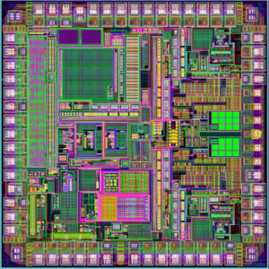
Copy Microcontroller PIC16F627A Binary
We can Copy Microcontroller PIC16F627A Binary, please view the Microcontroller PIC16F627A features for your reference:
High Performance RISC CPU:
Operating speeds from DC – 20 MHz
Interrupt capability
Direct, Indirect and Relative Addressing modes
35 single word instructions
– All instructions single cycle except branches
Special Microcontroller Features:
· Internal and external oscillator options
– Precision Internal 4 MHz oscillator factory calibrated to ±1%
– Low Power Internal 37 kHz oscillator
– External Oscillator support for crystals and resonators
· Power saving SLEEP mode
· Programmable weak pull-ups on PORTB
· Multiplexed Master Clear/Input-pin
· Watchdog Timer with independent oscillator for reliable operation
· Low voltage programming
· In-Circuit Serial Programming™ (via two pins)
· Programmable code protection
· Brown-out Reset
· Power-on Reset
· Power-up Timer and Oscillator Start-up Timer
· Wide operating voltage range. (2.0 – 5.5V)
· Industrial and extended temperature range
· High Endurance FLASH/EEPROM Cell
– 100,000 write FLASH endurance
– 1,000,000 write EEPROM endurance
Low Power Features:
· Standby Current:
– 100 nA @ 2.0V, typical
· Operating Current:
– 12 µA @ 32 kHz, 2.0V, typical
– 120 µA @ 1 MHz, 2.0V, typical
· Watchdog Timer Current
– 1 µA @ 2.0V, typical
· Timer1 oscillator current:
– 1.2 µA @ 32 kHz, 2.0V, typical
· Dual Speed Internal Oscillator:
– Run-time selectable between 4 MHz and 37 kHz
– 4 µs wake-up from SLEEP, 3.0V, typical
Peripheral Features:
· 16 I/O pins with individual direction control
· High current sink/source for direct LED drive
· Analog comparator module with:
– Two analog comparators
– Programmable on-chip voltage reference (VREF) module
– Selectable internal or external reference
– Comparator outputs are externally accessible
· Timer0: 8-bit timer/counter with 8-bit programmable prescaler
· Timer1: 16-bit timer/counter with external crystal/clock capability
· Timer2: 8-bit timer/counter with 8-bit period register, prescaler and postscaler
· Capture, Compare, PWM module
– 16-bit Capture/Compare
– 10-bit PWM
· Addressable Universal Synchronous/Asynchronous Receiver/Transmitter USART/SCI