 Attack Microcontroller TMS320C32PCM40 Firmware
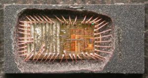
Attack Microcontroller TMS320C32PCM40 Firmware
We can Attack Microcontroller TMS320C32PCM40 Firmware, please view below Microcontroller TMS320C32PCM40 features for your reference:
High-Performance Floating-Point DSP
– TMS320C32-60 (5 V)
33-ns Instruction Cycle Time
330 Million Operations Per Second (MOPS), 60 Million Floating-Point Operations Per Second (MFLOPS), 30 Million Instructions Per Second (MIPS)
– TMS320C32-50 (5 V)
40-ns Instruction Cycle Time
275 MOPS, 50 MFLOPS, 25 MIPS
– TMS320C32-40 (5 V)
50-ns Instruction Cycle Time 220 MOPS, 40 MFLOPS, 20 MIPS
32-Bit High-Performance CPU
16- / 32-Bit Integer and 32- / 40-Bit
Floating-Point Operations
32-Bit Instruction Word, 24-Bit Addresses
Two 256 × 32-Bit Single-Cycle, Dual-Access
On-Chip RAM Blocks
Flexible Boot-Program Loader to Unlocking Microcontroller
On-Chip Memory-Mapped Peripherals:
– One Serial Port
– Two 32-Bit Timers
– Two-Channel Direct Memory Access (DMA) Coprocessor With Configurable Priorities
Enhanced External Memory Interface That Supports 8- / 16- / 32-Bit-Wide External RAM for Data Access and Program Execution From 16- / 32-Bit-Wide External RAM
TMS320C30 and TMS320C31 Object Code Compatible Fabricated using 0.7 µm Enhanced Performance Implanted CMOS (EPIC)
Technology by Texas Instruments (TI) 144-Pin Plastic Quad Flat Package ( PCM Suffix ) 5 V Eight Extended-Precision Registers
Two Address Generators With Eight
Auxiliary Registers and Two Auxiliary
Register Arithmetic Units (ARAUs)
Two Low-Power Modes
Two- and Three-Operand Instructions
Parallel Arithmetic Logic Unit (ALU) and
Multiplier Execution in a Single Cycle
Block-Repeat Capability
Zero-Overhead Loops With Single-Cycle
Branches
Conditional Calls and Returns
Interlocked Instructions for
Multiprocessing Support
One External Pin, PRGW, That Configures the External-Program-Memory Width to 16 or 32 Bits
Two Sets of Memory Strobes (STRB0 and STRB1) and One I / O Strobe (IOSTRB)
Allow Zero-Glue Logic Interface to Two
Banks of Memory and One Bank of External
Peripherals
Separate Bus-Control Registers for Each
Strobe-Control Wait-State Generation,
External Memory Width, and Data Type Size
STRB0 and STRB1 Memory Strobes Handle 8-, 16-, or 32-Bit External Data Accesses (Reads and Writes)
Multiprocessor Support Through the HOLD and HOLDA Signals Is Valid for All Strobes