 Decrypt IC Flash
Decrypt IC Flash memory, reset the Microcontroller security fuse bit when crack microcontroller using focus ion beam, and extract IC flash memory code in the format of heximal;
Decrypt IC Flash memory, reset the Microcontroller security fuse bit when crack microcontroller using focus ion beam, and extract IC flash memory code in the format of heximal
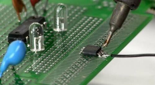
Invasive MCU breaking start with partial or full removal of the chip package in order to expose the silicon die. There are several methods, depending upon the package type and the requirements for further analysis. For microcontrollers, partial decapsulation is normally used, so that the device can be placed in a standard programmer unit and tested.
Some devices cannot be decapsulated and still maintain their electrical integrity. In this case the chip die has to be bonded to a chip carrier using a bonding machine which connects to the bonding pads on the die with thin aluminium or gold wire. Such bonding machines are available from different manufacturers and can be bought second-hand for less than £5,000. The contacts to the die can be also established using microprobing needles on a probing station.
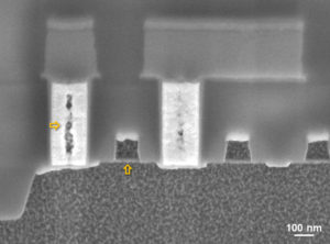
To undertake further work under a FIB or a SEM the chip surface has to be coated with a thin gold layer making it conductive, otherwise it will very quickly accumulate charge and the picture become dark. We used an Emitech K550 gold sputter coater to coat samples prior to the FIB work. Some modern FIB machines have a built-in video camera for optical navigation, eliminating the need for the special coating.
PCB Reverse Engineering Primary Objective
PCB Reverse Engineering primary objective is the development of unrestricted technical data, adequate for competitive procurement, through engineering evaluations of existing hardware.
In Process Reviews (IPRs) should be performed at the end of each principal phase of the PCB card cloning process to assure compliance to the process and to evaluate the need for continuing reverse engineering on the item.
a. Functional/economic analysis should be completed to collect available documentation, determine missing data requirements, determine testing requirements, and develop the PCB board Reverse Engineering Cost-Estimates and Schedules;
b. A disassembly procedure should be completed for each candidate to ensure functional integrity is maintained to allow for a viable analysis and documentation;
c. A reverse engineering management plan should be completed for each candidate to ensure a logical sequence of events to prevent delays or misinterpretations in the overall program objectives;
d. A hardware analysis should be performed to develop the missing data required for Level 3 drawings by restoring schematic diagram of circuit board;
e. Level 3 drawings are the result of the reverse engineering process and contain the documented parameters necessary to reproduce the selected candidate;
f. A quality control study should be performed and documented on the Level 3 drawings and prototypes of candidates to certify their compliance with original candidate specifications;
g. A production review should be performed to determine the economics of production of the reverse engineered item;
h. Prototype production involves the manufacture and testing of prototypes to determine if they meet all required specifications; and
i. A finalized TDP should be formulated and delivered to the Government/Tasking Agency requesting the reverse engineering of the candidate item.
Article quote from MLK-HDBK-115A(ARMY)
Break MCU ATmega1280V Eeprom
Break MCU ATmega1280V Eeprom memory for its data, and flash memory for its program, then extract files from both Microcontroller memories, disable the fuse bit by Microprocessor cracking;
Break MCU ATmega1280V Eeprom memory for its data, and flash memory for its program, then extract files from both Microcontroller memories, disable the fuse bit by Microprocessor cracking
Please view the MCU ATMEGA1280V features for your reference:
To program and verify the AT89S53 in the parallel programming mode, the following sequence is recommended after break MCU eeprom:
Power-up sequence:
Apply power between VCC and GND pins.
Set RST pin to “H”.
Apply a 3 MHz to 24 MHz clock to XTAL1 pin and wait for at least 10 milliseconds to break MCU dsPIC30F4011 eeprom.
Set PSEN pin to “L”
ALE pin to “H”
EA pin to “H” and all other pins to “H”.
Apply the appropriate combination of “H” or “L” logic levels to pins P2.6, P2.7, P3.6, P3.7 to select one of the programming operations shown in the eeprom Programming Modes table.
Apply the desired byte address to pins P1.0 to P1.7 and P2.0 to P2.5.
Apply data to pins P0.0 to P0.7 for Write Code operation.
Raise EA/VPP to 12V to enable eeprom programming, erase or verification.
Pulse ALE/PROG once to program a byte in the Code memory array, or the lock bits. The byte-write cycle is self-timed and typically takes 1.5 ms.
To verify the byte just programmed, bring pin P2.7 to “L” and read the programmed data at pins P0.0 to P0.7.
Repeat steps 3 through 7 changing the address and data for the entire 12K-byte array or until the end of the object file is reached.
Power-off sequence will affect the process of break MCU SAF-C164CI-8EM firmware eeprom:
Set XTAL1 to “L”.
Set RST and EA pins to “L”.
Turn VCC power off.
The AT89S53 features DATA Polling to indicate the end of a write cycle. During a write cycle in the parallel or serial programming mode, an attempted read of the last byte written will result in the complement of the written datum on P0.7 (parallel mode), and on the MSB of the serial output byte on MISO (serial mode).
Once the write cycle has been completed, true data are valid on all outputs, and the next cycle may begin. DATA Polling may begin any time after a write cycle has been initiated.
The progress of byte programming in the parallel programming mode can also be monitored by the RDY/BSY output signal. Pin P3.4 is pulled Low after ALE goes High during programming to indicate BUSY. P3.4 is pulled High again when programming is done to indicate READY.
PCB Reverse Engineering Rationale
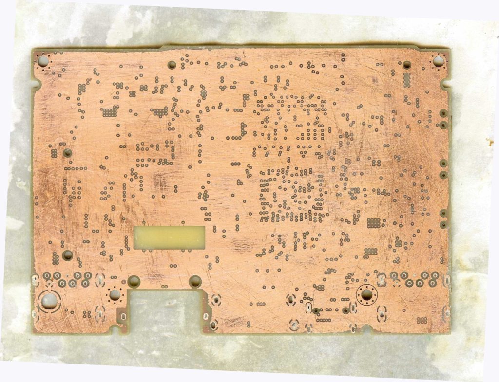
PCB Reverse Engineering Rationale is to extract wiring diagram from existing printed circuit board which has been out of production or not easy to get access to the new purchasing due to various reasons;
One method of controlling the high costs of replenishment spares is by pcb reverse engineering.
PCB Reverse engineering is the process of duplicating an item, functionally and dimensionally, by physically examining and measuring existing parts to develop the technical data (physical and material characteristics) required for competitive procurement.
The PCB reverse engineering process may be performed on specific items which are currently purchased sole-source. This may be due to limited data rights, in inadequate TDP, a diminished or non-existent source of supply, or as part of a Product Improvement Program (PIP).
Normally, PCB card cloning will not be cost effective unless the items under consideration are of a high dollar value or are procured in large quantities. Such items may be reverse engineered if an economical savings over their acquisition life cycle is demonstrated, and if other methods of acquiring the necessary technical data for competitive reprocurement are either more costly or not available.
Article quote from MLK-HDBK-115A(ARMY)
Reverse Engineering Microcomputer ATmega2560 Program
Reverse Engineering Microcomputer ATmega2560 internal memory, and extract MCU ATmega2560 Program out from flash memory, crack Microcontroller ATmega2560 security fuse bit by focus ion beam technique;
Reverse Engineering Microcomputer ATmega2560 internal memory, and extract MCU ATmega2560 Program out from flash memory, crack Microcontroller ATmega2560 security fuse bit by focus ion beam technique
If lock bits LB1 and LB2 have not been programmed, the programmed Code can be read back via the address and data lines for verification. The state of the lock bits can also be verified directly in the parallel programming mode when copying infineon saf-xc888cm-8ffi binary.
In the serial programming mode, the state of the lock bits can only be verified indirectly by observing that the lock bit features are enabled. In the parallel programming mode, Microcomputer erase is initiated by using the proper combination of control signals and by holding ALE/PROG low for 10 ms.
The Code array is written with all “1”s in the Microcomputer Erase operation. In the serial programming mode, a Microcomputer erase operation is initiated by issuing the Microcomputer Erase instruction. In this mode, Microcomputer erase is self-timed and takes about 16 ms.
During Microcomputer erase, a serial read from any address location will return 00H at the data outputs. A programmable fuse is available to disable Serial Programming if the user needs maximum system security after recover Microcomputer C8051F340 firmware.
The Serial Programming Fuse can only be programmed or erased in the Parallel Programming Mode. The AT89S53 is shipped with the Serial Programming Mode enabled.
Reading the Signature Bytes: The signature bytes are read by the same procedure as a normal verification of locations 030H and 031H, except that P3.6 and P3.7 must be pulled to a logic low. The values returned are as follows:
(030H) = 1EH indicates manufactured by Atmel
(031H) = 53H indicates 89S53
Every code byte in the program array can be written, and the entire array can be erased, by using the appropriate combination of control signals. The write operation cycle is self-timed and once initiated, will automatically time itself to completion.
All major programming vendors offer worldwide support for the Atmel microcontroller series. Please contact your local programming vendor for the appropriate software revision.
PCB Reverse Engineering Background in the U.S. department of Defense
PCB Reverse Engineering Background has a profound effect over the past years which is helping the engineer to restore circuit board schematic diagram from original physical samples include the gerber file, layout drawing and BOM list;
Defense contractors who supply systems, equipment and spare parts during the initial production phase of a weapon system acquisition in which they have performed in the development, frequently become the “sole-source” for follow-on procurements.
The cost of items procured under these sole source conditions are sometimes inflated beyond their true value. Consequently, procurement costs for spare parts consume an increasingly larger share of the defense dollar. Recent emphasis on the prices paid for spare parts dictates the need for competition.
Congress and the Department of Defense (DOD) directed the military services to increase competition in an effort to reduce the cost of spare parts. The Defense Acquisition Regulation Supplement No. 6 (DAR-S6), dated 1 June 1983, titled: DOD Replenishment Parts Breakout Program, was promulgated to encourage competition and reduce restrictive features which limit competitive procurement.
Article quote from MLK-HDBK-115A(ARMY)
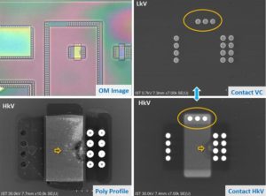
Reverse Engineering IC Flash
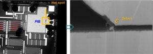
Reverse Engineering IC Flash is starting point of Microcontroller reverse engineering, target MCU will be delayer one by one in the reverse order of Microprocessor manufacturing, the purpose is to figure out the security fuse bit and cut it off;
Reverse Engineering IC Flash is starting point of Microcontroller reverse engineering, target MCU will be delayer one by one in the reverse order of Microprocessor manufacturing, the purpose is to figure out the security fuse bit and cut it off
Read program and data out from Microcontroller memory requires direct access to the internal components of the device. If it is a security module or a USB dongle, then it has to be opened to get access to the internal memory chips. In the case of a smartcard or a microcontroller, the packaging should be removed followed by FIB or laser depassivation to get access to the internal wires buried deep under the passivation layer of the chip.
Such ic decryption method normally require a well equipped and knowledgeable ic attacker to succeed. Meanwhile, invasive ic extraction are becoming constantly more demanding and expensive, as feature sizes shrink and device complexity increases.
Decode MCU ATmega2560V Program
Decode MCU ATmega2560V Program from encrypted flash memory is a process of Microcontroller firmware extraction, reset the status of microprocessor ATmega2560V by unlocking;
We can decode mcu ATMEGA2560V program, please view the mcu ATMEGA2560V features for your reference:
The Code memory array can be programmed using the serial SPI bus while RST is pulled to VCC. The serial interface consists of pins SCK, MOSI (input) and MISO (output) when copy mcu at89c55wd binary.
After RST is set high, the Programming Enable instruction needs to be executed first before program/erase operations can be executed. An auto-erase cycle is built into the self-timed programming operation (in the serial mode ONLY) and there is no need to first execute the Chip Erase instruction unless any of the lock bits have been programmed.
The Chip Erase operation turns the content of every memory location in the Code array into FFH. The Code memory array has an address space of 0000H to 2FFFH.
Either an external system clock is supplied at pin XTAL1 or a crystal needs to be connected across pins XTAL1 and XTAL2. The maximum serial clock (SCK) frequency should be less than 1/40 of the crystal frequency. With a 24 MHz oscillator clock, the maximum SCK frequency is 600 kHz. To program and verify the AT89S53 in the serial programming mode, the following sequence is recommended:
Power-up sequence: Apply power between VCC and GND pins. Set RST pin to “H”. If a crystal is not connected across pins XTAL1 and XTAL2, apply a 3 MHz to 24 MHz clock to XTAL1 pin and wait for at least 10 milliseconds if attack mcu atmega162 flash program.
Enable serial programming by sending the Programming Enable serial instruction to pin MOSI/P1.5. The frequency of the shift clock supplied at pin SCK/P1.7 needs to be less than the CPU clock at XTAL1 divided by 40..
The Code array is programmed one byte at a time by supplying the address and data together with the appropriate Write instruction.
The selected memory location is first automatically erased before new data is written. The write cycle is self-timed and typically takes less than 2.5 ms at 5V. Any memory location can be verified by using the Read instruction which returns the content at the selected address at serial output MISO/P1.6 before attack microcontroller w77e058a40dl flash program.
At the end of a programming session, RST can be set low to commence normal operation. Power-off sequence (if needed): Set XTAL1 to “L” (if a crystal is not used). Set RST to “L”. Turn VCC power off.
Break IC Flash
Break IC flash could be also applied to the device communication protocol in order to find any hidden functions embedded by the software developer for testing and upgrade purposes.
Break IC flash could be also applied to the device communication protocol in order to find any hidden functions embedded by the software developer for testing and upgrade purposes
IC Chip manufacturers very often embed hardware test interfaces for postproduction testing of their semiconductor devices. If the security protection for these interfaces is not properly designed, the ic attacker can exploit it to get access to the on-chip memory. In smartcards such test interfaces are normally located outside the chip circuit and physically removed after the test operation, eliminating any possibility of use by outsiders.
Any security system, either software or hardware, could also have holes in its design and there is always a small chance that an ic cloner would eventually find one with brute force random testing. Careful design of the security protection, followed by proper evaluation, could help avoid many problems and make such MCU attack virtually impossible.
Read IC Program
Another possible brute force ic decryption when you are trying to Read IC Program, applicable to many semiconductor chips, is applying an external high voltage signal (normally twice the power supply) to the chip’s pins to find out whether one of them has any transaction like entering into a factory test or programming mode.
Another possible brute force ic decryption when you are trying to Read IC Program, applicable to many semiconductor chips, is applying an external high voltage signal (normally twice the power supply) to the chip’s pins to find out whether one of them has any transaction like entering into a factory test or programming mode
In fact, such pins can be easily found with a digital multimeter because they do not have a protection diode to the power supply line. Once sensitivity to a high voltage is found for any pin, MCU Cracker can try a systematic search on possible combinations of logic signals applied to other pins to figure out which of them are used for the test/programming mode and exploit this opportunity.