 Decrypt Secured MCU ATmega128P Code
 November 17th, 2012 |
  Author:
 We can decrypt secured MCU ATMEGA128P code, please view the secured MCU ATMEGA128P features for your reference:
The following charts show typical behavior. These data are characterized but not tested. All current consumption measurements are performed with all I/O pins configured as inputs and with internal pull-ups enabled.
The current consumption is a function of several factors such as: Operating voltage, operating frequency, loading of I/O pins, switching rate of I/O pins, code executed and ambient temperature. The dominating factors are operating voltage and frequency if Decrypt Secured MCU ATMEGA128P Code.
The current drawn from capacitive loaded pins may be estimated (for one pin) as CL·VCC·f where CL = load capacitance, VCC = operating voltage and f = average switching frequency of I/O pin.
The difference between current consumption in Power-down mode with Watchdog Timer enabled and Power-down mode with Watchdog Timer disabled represents the differential current drawn by the Watchdog Timer after Decrypt Secured MCU ATMEGA128P Code.
The ATMEGA128P is a low-power, high-performance CMOS 8-bit microcomputer with 12K bytes of Downloadable Flash codemable and erasable read only memory.
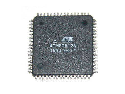
The device is manufactured using Atmel’s high density nonvolatile memory technology and is compatible with the industry standard 80C51 instruction set and pinout.
The onsecured MCU Downloadable Flash allows the code memory to be recodemed in-system through an SPI serial interface or by a conventional nonvolatile memory codemer before Decrypt Secured MCU ATMEGA128P Code.
Smartcard attacker fight with service provider
Smartcard attack will not be so expensive, because pirate devices are normally based on standard microcontrollers which have much lower security protection than pay-TV smartcards. Very likely the device will be cracked in a few weeks, and the secondary attackers will flood the market with their clones. Fairly soon, the information on how to build pirate devices becomes available on the Internet and anyone can build pirate devices at almost no cost. So the pay-TV service provider loses millions of dollars; sometimes the original attacker is sued or prosecuted. But because the lost profit was distributed among all the pirates and dishonest subscribers, the service provider hardly gets any money back. The only effect of such actions is to threaten the hacker community with punishment. In addition the service provider will have to spend a fortune on redesigning his access control system, choosing and developing software for the new smartcard, and distributing cards to the subscribers
 Posted in Break IC |
  Tags: decode smartcard, discover smartcard, hack smartcard, recover smartcard |
  Comments Closed
Pay-TV access card attack
Another example is when the smartcard attacker invests a huge amount of money to reverse engineer a pay-TV access card. Then he disassembles the internal code from the card, learning everything that happens during authorisation and operation. Very likely he would be able to find vulnerabilities which give unlimited access to the subscription channels, for example, by applying a power glitch at just the right moment to cause a malfunction of the CPU. Once he succeeded he could either offer the subscription service at a very competitive price, or sell equipment for counterfeiting the card to malicious people. Obviously such an attacker needs to invest some capital to do this. But once he launches a pirate device on the market, it will be attacked by others.
Posted in Break IC |
Tags: break smartcard, decrypt smartcard, extract smartcard, smartcard attack, smartcard crack |
Comments Closed
modem- or network-card adapt to PC condition
Anyone who has ever tried to add a modem- or network-card to a PC knows that such an undertaking may produce unwanted results and can take more time than expected. To achieve cost savings from high volume production, the add-in board is designed to be logically compatible to a large variety of motherboards from various vendors. This flexibility makes it necessary to configure the board for its operating environment before it is ready to function. To perform the configuration one needs two pieces of information: sufficient knowledge of the system that the board is expected to reside in and knowledge of the board itself. Once the suitable settings are determined one needs to set jumpers or flip switches on the board. This completes the tricky part of the hardware installation.
Dump Microcontroller ATMEGA128V Locked Code
We can dump microcontroller ATMEGA128V locked code, please view the microcontroller ATMEGA128V features for your reference:
The ATMEGA128V provides the following standard features: 12K bytes of Downloadable locked code, 256 bytes of RAM, 32 I/O lines, programmable watchdog timer, two Data Pointers, three 16-bit timer/counters, a six-vector two-level interrupt architecture, a full duplex serial port, on-chip oscillator, and clock circuitry.
In addition, the ATMEGA128V is designed with static logic for operation down to zero frequency and supports two software selectable power saving modes. The Idle Mode stops the CPU while allowing the RAM, timer/counters, serial port, and interrupt system to continue functioning if Dump Microcontroller ATMEGA128V Locked Code.
The Power Down Mode saves the RAM contents but freezes the oscillator, disabling all other chip functions until the next interrupt or hardware reset.
The Downloadable locked code can be changed a single byte at a time and is accessible through the SPI serial interface. Holding RESET active forces the SPI bus into a serial programming interface and allows the program memory to be written to or read from unless Lock Bit 2 has been activated after Dump Microcontroller ATMEGA128V Locked Code.
Port 0 is an 8-bit open drain bidirectional I/O port. As an output port, each pin can sink eight TTL inputs. When 1s are written to port 0 pins, the pins can be used as high impedance inputs. Port 0 can also be configured to be the multiplexed low order address/data bus during accesses to external program and data memory. In this mode, P0 has internal pullups.
Port 0 also receives the code bytes during locked code programming and outputs the code bytes during program verification. External pullups are required during program verification before Dump Microcontroller ATMEGA128V Locked Code.
Port 1 is an 8-bit bidirectional I/O port with internal pullups. The Port 1 output buffers can sink/source four TTL inputs. When 1s are written to Port 1 pins, they are pulled high by the internal pullups and can be used as inputs. As inputs, Port 1 pins that are externally being pulled low will source current (IIL) because of the internal pullups.
Some Port 1 pins provide additional functions. P1.0 and P1.1 can be configured to be the timer/counter 2 external count input (P1.0/T2) and the timer/counter 2 trigger input (P1.1/T2EX), respectively after REVERSE ENGINEERING MICROCONTROLLER.
Recover Locked Chip ATMEGA128PV Binary
We can recover locked chip ATMEGA128PV binary, please view the locked chip ATMEGA128PV features for your reference:
Port 1 also receives the low-order address bytes during Flash programming and verification.
Port 2
Port 2 is an 8-bit bidirectional I/O port with internal pullups. The Port 2 output buffers can sink/source four TTL inputs. When 1s are written to Port 2 pins, they are pulled high by the internal pullups and can be used as inputs when Recover Locked Chip ATMEGA128PV Binary.
As inputs, Port 2 pins that are externally being pulled low will source current (IIL) because of the internal pullups. Port 2 emits the high-order address byte during fetches from external program memory and during accesses to external data memory that use 16-bit addresses (MOVX @ DPTR).
In this application, Port 2 uses strong internal pullups when emitting 1s. During accesses to external data memory that use 8-bit addresses (MOVX @ RI), Port 2 emits the contents of the P2 Special Function Register.
Port 2 also receives the high-order address bits and some control signals during Flash programming and verification.
Port 3
Port 3 is an 8 bit bidirectional I/O port with internal pullups. The Port 3 output buffers can sink/source four TTL inputs. When 1s are written to Port 3 pins, they are pulled high by the internal pullups and can be used as inputs after Recover Locked Chip ATMEGA128PV Binary.
As inputs, Port 3 pins that are externally being pulled low will source current (IIL) because of the pullups. Port 3 also serves the functions of various special features of the AT89S53, as shown in the following table. Port 3 also receives some control signals for Flash programming and verification.
Reset input. A high on this pin for two machine cycles while the oscillator is running resets the device.
ALE/PROG
Address Latch Enable is an output pulse for latching the low byte of the address during accesses to external memory. This pin is also the program pulse input (PROG) during Flash programming.
In normal operation, ALE is emitted at a constant rate of 1/6 the oscillator frequency and may be used for external timing or clocking purposes. Note, however, that one ALE pulse is skipped during each access to external data memory before RECOVER MCU.
Decrypt Locked MCU ATMEGA128V Embedded Firmware
We can decrypt locked MCU ATMEGA128V embedded firmware, please view the locked MCU ATMEGA128V features for your reference:
If desired, ALE operation can be disabled by setting bit 0 of SFR location 8EH. With the bit set, ALE is active only during a MOVX or MOVC instruction. Otherwise, the pin is weakly pulled high. Setting the ALE-disable bit has no effect if the microcontroller is in external execution mode.
Program Store Enable is the read strobe to external program memory. When the AT89S53 is executing embedded firmware from external program memory, PSEN is activated twice each machine cycle, except that two PSEN activations are skipped during each access to external data memory before Decrypt Locked MCU ATMEGA128V Embedded Firmware.
External Access Enable. EA must be strapped to GND in order to enable the device to fetch embedded firmware from external program memory locations starting at 0000H up to FFFFH. Note, however, that if lock bit 1 is programmed, EA will be internally latched on reset.
EA should be strapped to VCC for internal program executions. This pin also receives the 12-volt programming enable voltage (VPP) during Flash programming when 12-volt programming is selected.
A map of the on-chip memory area called the Special Function Register (SFR) space is shown in Table 1. Note that not all of the addresses are occupied, and unoccupied addresses may not be implemented on the chip when Decrypt Locked MCU ATMEGA128V Embedded Firmware.
Read accesses to these addresses will in general return random data, and write accesses will have an indeterminate effect. User software should not write 1s to these unlisted locations, since they may be used in future products to invoke new features. In that case, the reset or inactive values of the new bits will always be 0.
Timer 2 Registers Control and status bits are contained in registers T2CON (shown in Table 2) and T2MOD (shown in Table 9) for Timer 2. The register pair (RCAP2H, RCAP2L) are the Capture/Reload registers for Timer 2 in 16 bit capture mode or 16-bit auto-reload mode before Decrypt Locked MCU ATMEGA128V Embedded Firmware.
Watchdog Control Register The WCON register contains control bits for the Watchdog Timer (shown in Table 3). The DPS bit selects one of two DPTR registers available after BREAK IC.
Decrypt Microprocessor ATMEGA169PA Code
We can decrypt Microprocessor ATMEGA169PA code, please view the Microprocessor ATMEGA169PA features for your reference:
SPI Registers Control and status bits for the Serial Peripheral Interface are contained in registers SPCR (shown in Table 4) and SPSR (shown in Table 5). The SPI data bits are contained in the SPDR register.
Writing the SPI data register during serial data transfer sets the Write Collision bit, WCOL, in the SPSR register. The SPDR is double buffered for writing and the values in SPDR are not changed by Reset if decrypt Microprocessor code.
Interrupt Registers The global interrupt enable bit and the individual interrupt enable bits are in the IE register. In addition, the individual interrupt enable bit for the SPI is in the SPCR register. Two priorities can be set for each of the six interrupt sources in the IP register before Decrypt Microprocessor ATMEGA169PA Code.
Dual Data Pointer Registers To facilitate accessing external data memory, two banks of 16 bit Data Pointer Registers are provided: DP0 at SFR address locations 82H-83H and DP1 at 84H-85H. Bit DPS = 0 in SFR WCON selects DP0 and DPS = 1 selects DP1.
The user should always initalize the DPS bit to the appropriate value before accessing the respective Data Pointer register.
Power Off Flag The Power Off Flag (POF) is located at bit_4 (PCON.4) in the PCON SFR. POF is set to “1” during power up. It can be set and reset under software control and is not affected by RESET when Decrypt Microprocessor ATMEGA169PA Code.
The ATMEGA169PA implements 256 bytes of RAM. The upper 128 bytes of RAM occupy a parallel space to the Special Function Registers. That means the upper 128 bytes have the same addresses as the SFR space but are physically separate from SFR space.
When an instruction accesses an internal location above address 7FH, the address mode used in the instruction specifies whether the CPU accesses the upper 128 bytes of RAM or the SFR space. Instructions that use direct addressing access SFR space.
For example, the following direct addressing instruction accesses the SFR at location 0A0H (which is P2) after Decrypt Microprocessor ATMEGA169PA Code.
Recover Microcontroller ATmega169PV Heximal
We can recover Microcontroller ATmega169PV heximal, please view the Microcontroller ATmega169PV features for your reference:
Instructions that use indirect addressing access the upper 128 bytes of RAM. For example, the following indirect addressing instruction, where R0 contains 0A0H, accesses the data byte at address 0A0H, rather than P2 (whose address is 0A0H).
MOV @R0, #data Note that stack operations are examples of indirect addressing, so the upper 128 bytes of data RAM are available as stack space if Recover Microcontroller ATMEGA169PV Heximal.
The programmable Watchdog Timer (WDT) operates from an independent oscillator. The prescaler bits, PS0, PS1 and PS2 in SFR WCON are used to set the period of the Watchdog Timer from 16 ms to 2048 ms.
The available timer periods are shown in the following table and the actual timer periods (at VCC = 5V) are within ±30% of the nominal. The WDT is disabled by Power-on Reset and during Power Down.
It is enabled by setting the WDTEN bit in SFR WCON (address = 96H). The WDT is reset by setting the WDTRST bit in WCON. When the WDT times out without being reset or disabled, an internal RST pulse is generated to reset the CPU before Recover Microcontroller ATMEGA169PV Heximal.
Timer 0 and Timer 1 in the ATMEGA169PV operate the same way as Timer 0 and Timer 1 in the ATMEGA169PV. For further information, see the October 1995 IC Data Book, page 2-45, section titled, “Timer/Counters.”
Timer 2 is a 16 bit Timer/Counter that can operate as either a timer or an event counter.
The type of operation is selected by bit C/T2 in the SFR T2CON (shown in Table 2). Timer 2 has three operating modes: capture, auto-reload (up or down counting), and baud rate generator.
The modes are selected by bits in T2CON, as shown in Table 8. Timer 2 consists of two 8-bit registers, TH2 and TL2.
In the Timer function, the TL2 register is incremented every machine cycle. Since a machine cycle consists of 12 oscillator periods, the count rate is 1/12 of the oscillator frequency before Recover Microcontroller ATMEGA169PV Heximal.
Break MCU ATMEGA2560PV Code
We can break MCU ATMEGA2560PV code, please view the MCU ATMEGA2560PV features for your reference:
Timer 2 is a 16 bit Timer/Counter that can operate as either a timer or an event counter. The type of operation is selected by bit C/T2 in the SFR T2CON (shown in Table 2). Timer 2 has three operating modes: capture, auto-reload (up or down counting), and baud rate generator.
The modes are selected by bits in T2CON, as shown in Table 8. Timer 2 consists of two 8-bit registers, TH2 and TL2. In the Timer function, the TL2 register is incremented every machine cycle. Since a machine cycle consists of 12 oscillator periods, the count rate is 1/12 of the oscillator frequency if Break MCU ATMEGA2560PV Code.
In the Counter function, the register is incremented in response to a 1-to-0 transition at its corresponding external input pin, T2. In this function, the external input is sampled during S5P2 of every machine cycle. When the samples show a high in one cycle and a low in the next cycle, the count is incremented.
The new count value appears in the register during S3P1 of the cycle following the one in which the transition was detected. Since two machine cycles (24 oscillator periods) are required to recognize a 1-to-0 transition, the maximum count rate is 1/24 of the oscillator frequency after Break MCU ATMEGA2560PV Code.
To ensure that a given level is sampled at least once before it changes, the level should be held for at least one full machine cycle. In the capture mode, two options are selected by bit EXEN2 in T2CON. If EXEN2 = 0, Timer 2 is a 16 bit timer or counter which upon overflow sets bit TF2 in T2CON.
This bit can then be used to generate an interrupt. If EXEN2 = 1, Timer 2 performs the same operation, but a l to-0 transition at external input T2EX also causes the current value in TH2 and TL2 to be captured into RCAP2H and RCAP2L, respectively if break MCU code.
In addition, the transition at T2EX causes bit EXF2 in T2CON to be set. The EXF2 bit, like TF2, can generate an interrupt after Break MCU ATMEGA2560PV Code.