 Decode Secured Atmel Chip ATmega164A Heximal
 December 30th, 2012 |
  Author:
 We can decode secured Atmel Chip ATMEGA164A heximal, please view the secured Atmel Chip ATMEGA164A features for your reference:
Thus, when the BOD is not enabled, after setting the AINBG bit, the user must always allow the reference to start-up before the output from the Analog Comparator is used when decode secured Atmel Chip heximal.
The bandgap reference uses typically 10 µA, and to reduce power consumption in Power-down mode, the user can avoid the three conditions above to ensure that the reference is turned off before entering Power-down mode if Decode Secured Atmel Chip ATmega164A Heximal.
The ATtiny15L has two 8-bit Interrupt Mask control registers: GIMSK (General Interrupt Mask register) and TIMSK (Timer/Counter Interrupt Mask register) before decode secured Atmel Chip heximal.
When an interrupt occurs, the Global Interrupt Enable I-bit is cleared (zero) and all interrupts are disabled. The user software can set the I-bit (one) to enable interrupts. The Ibit is set (one) when a Return from Interrupt instruction (RETI) is executed.
When the heximal Counter is vectored to the actual interrupt vector in order to execute the interrupt handling routine, hardware clears the corresponding flag that generated the interrupt.
Some of the interrupt flags can also be cleared by writing a logical “1” to the flag bit position(s) to be cleared. If an interrupt condition occurs when the corresponding interrupt enable bit is cleared (zero), the interrupt flag will be set and remembered until the interrupt is enabled, or the flag is cleared by software if Decode Secured Atmel Chip ATmega164A Heximal.
If one or more interrupt conditions occur when the global interrupt enable bit is cleared (zero), the corresponding interrupt flag(s) will be set and remembered until the global interrupt enable bit is set (one), and will be executed by order of priority.
Note that external level interrupt does not have a flag, and will only be remembered for as long as the interrupt condition is present.
Note that the Status Register is not automatically stored when entering an interrupt routine and restored when returning from an interrupt routine. This must be handled by software if BREAK IC.
Reverse Engineering Locked Chip ATmega164PA Firmware
We can reverse engineering locked chip ATMEGA164PA firmware, please view the locked chip ATMEGA164PA features for your reference:
The interrupt execution response for all the enabled AVR interrupts is four clock cycles minimum. After the four clock cycles the firmware vector address for the actual interrupt handling routine is executed.
During this 4-clock-cycle period, the firmware Counter (9 bits) is pushed onto the Stack. The vector is often a relative jump to the interrupt routine, and this jump takes two clock cycles.
If an interrupt occurs during execution of a multi cycle instruction, this instruction is completed before the interrupt is served. If an interrupt occurs when the MCU is in Sleep mode, the interrupt execution response time is increased by four clock cycles before Reverse Engineering Locked Chip ATmega164PA Firmware.
A return from an interrupt handling routine takes four clock cycles. During these four clock cycles, the firmware Counter (9 bits) is popped back from the Stack. When AVR exits from an interrupt, it will always return to the main firmware and execute one more instruction before any pending interrupt is served.
· Bit 7 – Res: Reserved Bit
This bit is a reserved bit in the atmega164pa and always reads as zero.
· Bit 6 – INT0: External Interrupt Request 0 Enable
When the INT0 bit is set (one) and the I-bit in the Status Register (SREG) is set (one), the external pin interrupt is activated.
The Interrupt Sense Control0 bits 1/0 (ISC01 and ISC00) in the MCU general Control Register (MCUCR) define whether the external interrupt is activated on rising or falling edge, on pin change, or low level of the INT0 pin after Reverse Engineering Locked Chip ATmega164PA Firmware.
Activity on the pin will cause an interrupt request even if INT0 is configured as an output. The corresponding interrupt of External Interrupt Request 0 is executed from firmware memory address $001. See also “External Interrupts.”
· Bit 5 – PCIE: Pin Change Interrupt Enable
When the PCIE bit is set (one) and the I-bit in the Status Register (SREG) is set (one), the interrupt on pin change is enabled. Any change on any input or I/O pin will cause an interrupt.
The corresponding interrupt of Pin Change Interrupt Request is executed from firmware memory address $002. See also “Pin Change Interrupt.”
· Bits 4..0 – Res: Reserved Bits
These bits are reserved bits in the atmega164pa and always read as zero.
· Bit 6 – INTF0: External Interrupt Flag0
When an edge or logic change on the INT0 pin triggers an interrupt request, INTF0 becomes set (one). If the I-bit in SREG and the INT0 bit in GIMSK are set (one), the MCU will jump to the interrupt vector at address $001 before Reverse Engineering Locked Chip ATmega164PA Firmware.
The flag is cleared when the interrupt routine is executed. Alternatively, the flag can be cleared by writing a logical “1” to it. The flag is always cleared when INT0 is configured as level interrupt.
· Bit 5 – PCIF: Pin Change Interrupt Flag
When an event on any input or I/O pin triggers an interrupt request, PCIF becomes set (one). If the I-bit in SREG and the PCIE bit in GIMSK are set (one), the MCU will jump to the interrupt vector at address $002.
The flag is cleared when the interrupt routine is executed. Alternatively, the flag can be cleared by writing a logical “1” to it before reverse engineering Microcontroller.
· Bits 4..0 – Res: Reserved Bits
These bits are reserved bits in the atmega164pa and always read as zero.
Recover Locked Microprocessor ATmega164PV Source Code
We can recover locked microprocessor ATMEGA164PV source code, please view the locked microprocessor ATMEGA164PV features for your reference:
To enter any of the three sleep modes, the SE bit in locked microprocessorCR must be set (one) and a SLEEP instruction must be executed. The SM1 and SM0 bits in the locked microprocessorCR register select which sleep mode (Idle, ADC Noise Reduction or Power-down) will be activated by the SLEEP instruction (see Table 7).
If an enabled interrupt occurs while the locked microprocessor is in a sleep mode, the locked microprocessor wakes up. The locked microprocessor is then halted for four cycles, executes the interrupt routine and resumes execution from the instruction following SLEEP if Recover Locked Microprocessor ATmega164PV Source Code.
On wake-up from Power-down mode on pin change, the two instructions following SLEEP. The contents of the register file, SRAM, and I/O memory are unaltered when the device wakes up from sleep.
If a reset occurs during sleep mode, the locked microprocessor wakes up and executes from the Reset vector. When the SM1/SM0 bits are “00”, the SLEEP instruction forces the locked microprocessor into the Idle mode, stopping the CPU but allowing the ADC, Analog Comparator, Timer/Counters, Watchdog and the Interrupt system to continue operating.
This enables the locked microprocessor to wake up from external triggered interrupts as well as internal ones like the Timer Overflow interrupt and Watchdog Reset. If the ADC is enabled, a conversion starts automatically when this mode is entered when Recover Locked Microprocessor ATmega164PV Source Code.
If wake-up from the Analog Comparator interrupt is not required, the Analog Comparator can be powered down by setting the ADC-bit in the Analog Comparator Control and Status Register (ACSR).
This will reduce power consumption in Idle mode. When the SM1/SM0 bits are “01”, the SLEEP instruction forces the locked microprocessor into the ADC Noise Reduction mode, stopping the CPU but allowing the ADC, the external interrupt pin, pin change interrupt and the Watchdog (if enabled) to continue operating.
Please note that the clock system including the PLL is also active in the ADC Noise Reduction mode. This improves the noise environment for the ADC, enabling higher resolution measurements after RECOVER MCU.
If the ADC is enabled, a conversion starts automatically when this mode is entered. In addition to Watchdog Time-out and External Reset, only an external leveltriggered interrupt, a pin change interrupt or an ADC interrupt can wake up.
Break IC ATmega324V Protected Firmware
We can break IC ATMEGA324V protected firmware, please view the IC ATMEGA324V features for your reference:
The internal PLL in ATtiny15L generates a clock frequency that is 16x multiplied from the RC oscillator system clock. If the RC oscillator frequency is the nominal 1.6 MHz, the fast peripheral clock is 25.6 MHz.
The fast peripheral clock, or a clock prescaled from that, can be selected as the clock source for Timer/Counter1. The PLL is locked on the tunable internal RC oscillator and adjusting the tunable internal RC oscillator via the OSCCAL register will adjust the fast peripheral clock at the same time.
Timer1 may malfunction if the internal RC oscillator is adjusted beyond 1.75 MHz. It is recommended not to take the OSCCAL adjustments to a higher frequency than 1.75 MHz in order to keep proper operation of all chip functions before Break IC ATmega324V Protected Firmware.
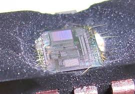
Break IC ATmega324V Protected Firmware
The ATmega324 provides two general purpose 8-bit Timer/Counters. The Timer/Counters hav e se par ate p re sc al ing s ele cti on fr om s epar at e 1 0- bit pres calers.
The Timer/Counter0 uses internal clock (CK) as the clock time base. The Timer/Counter1 may use either the internal clock (CK) or the fast peripheral clock (PCK) as the clock time base when break ic protected firmware.
The four prescaled selections are: CK/8, CK/64, CK/256, and CK/1024, where CK is the oscillator clock. CK, external source and stop, can also be selected as clock sources if Break IC ATmega324V Protected Firmware.
Setting the PSR10 bit in SFIOR resets the prescaler. This allows the user to operate with a predictable prescaler. Figure 19 shows the Timer/Counter1 prescaler.
For Timer/Counter1 the clock selections are: PCK, PCK/2, PCK/4, PCK/8, CK (=PCK/16), CK/2, CK/4, CK/8,CK/16, CK/32, CK/64, CK/128, CK/256, CK/512, CK/1024, and stop. The clock options are described in Table 12 on page 32 and the Timer/Counter1 Control Register (TCCR1).
Setting the PSR1 bit in the SFIOR register resets the 10-bit prescaler. This allows the user to operate with a predictable prescaler.
Reverse Engineering Secured Chip ATmega324 Flash
We can reverse engineering secured chip ATMEGA324 flash, please view the secured chip ATMEGA324 features for your reference:
When the SM1/SM0 bits are “10”, the SLEEP instruction forces the MCU into the Power down mode. Only an External Reset, a Watchdog Reset (if enabled), an external level triggered interrupt, or a pin change interrupt can wake up the MCU when reverse engineering secured chip flash.
Note that if a level-triggered or pin change interrupt is used for wake-up from Power-down mode, the changed level must be held for some time to wake up the MCU if reverse engineering secured chip flash.
This makes the MCU less sensitive to noise. The changed level is sampled twice by the Watchdog Oscillator clock, and if the input has the required level during this time, the MCU will wake up before reverse engineering secured chip flash.
The period of the waTchdog Oscillator is 2.9 µs (nominal) at 3.0V and 25°C. The frequency of the Watchdog Oscillator is voltage-dependent as shown in the “Electrical Characteristics” section after reverse engineering secured chip flash.
When waking up from the Power-down mode, a delay from the wake-up condition occurs until the wake-up becomes effective. This allows the clock to restart and become stable after having been stopped when reverse engineering secured chip flash.
The wake-up period is defined by the same CKSEL fuses that define the reset time-out period. The internal RC oscillator provides a fixed 1.6 MHz clock (nominal at 5V and 25°C) if reverse engineering secured chip flash.
This internal clock is always the system clock of the ATtiny15L. This oscillator can be calibrated by writing the calibration byte (see page 55) to the OSCCAL register before reverse engineering secured chip flash.
Writing the calibration byte to this address will trim the internal oscillator frequency in order to remove process variations. When OSCCAL is zero (initial value), the lowest available frequency is chosen after reverse engineering secured chip flash.
Writing non-zero values to this register will increase the frequency of the internal oscillator. Writing $FF to the register selects the highest available frequency before reverse engineering secured chip flash.
Decode Locked Microprocessor ATmega324A Source Code
We can decode locked microprocessor ATMEGA324A source code, please view the locked microprocessor ATMEGA324A features for your reference:
Writing a logical “1” to this bit forces a change in the compare match output pin PB1 (OC1A) according to the values already set in COM1A1 and COM1A0.
The Force Output Compare bit can be used to change the output pin without waiting for a compare match in timer.
The automatic action programmed in COM1A1 and COM1A0 happens as if a Compare Match had occurred, but no interrupt is generated and the Timer/Counter1 will not be cleared even if CTC1 is set. The FOC1A bit will always be read as zero if decode locked microprocessor source code.
The setting of the FOC1A bit has no effect in PWM mode.
· Bit 1 – PSR1: Prescaler Reset Timer/Counter1
When this bit is set (one) the Timer/Counter1 prescaler will be reset. The bit will be cleared by hardware after the operation is performed. Writing a “0” to this bit will have no effect. This bit will always be read as zero.
· Bit 0 – PSR0: Prescaler Reset Timer/Counter0
When this bit is set (one) the Timer/Counter0 prescaler will be reset. The bit will be cleared by hardware after the operation is performed. Writing a “0” to this bit will have no effect. This bit will always be read as zero after decode locked microprocessor source code.
The 8-bit Timer/Counter0 can select clock source from CK, prescaled CK or an external pin. In addition, it can be stopped as described in the specification for the Timer/Counter0 Control Register (TCCR0).
The overflow status flag is found in the Timer/Counter Interrupt Flag Register (TIFR). Control signals are found in the Timer/Counter0 Control Register (TCCR0). The interrupt enable/disable settings for Timer/Counter0 are found in the Timer/Counter Interrupt Mask Register (TIMSK) if decode locked microprocessor source code.
When Timer/Counter0 is externally clocked, the external signal is synchronized with the oscillator frequency of the CPU. To ensure proper sampling of the external clock, the minimum time between two external clock transitions must be at least one internal CPU clock period.
The external clock signal is sampled on the rising edge of the internal CPU clock. The 8-bit Timer/Counter0 features both a high-resolution and a high-accuracy usage with the lower prescaling opportunities.
Similarly, the high-prescaling opportunities make the Timer/Counter0 useful for lower-speed functions or exact-timing functions with infrequent actions before BREAK IC.
Recover Encrypted Processor ATmega1284P Heximal
We can recover encrypted processor ATMEGA1284P Heximal, please view the encrypted processor ATMEGA1284P features for your reference:
If the result is left-adjusted and no more than 8-bit precision is required, it is sufficient to read ADCH. Otherwise, ADCL must be read first, then ADCH, to ensure that the content of the data registers belongs to the same conversion when recover encrypted processor heximal.
Once ADCL is read, ADC access to data registers is blocked. This means that if ADCL has been read, and a conversion completes before ADCH is read, neither register is updated and the result from the conversion is lost if recover encrypted processor heximal.
When ADCH is read, ADC access to the ADCH and ADCL registers is re-enabled. The ADC has its own interrupt, which can be triggered when a conversion completes. When ADC access to the data registers is prohibited between reading of ADCH and ADCL, the interrupt will trigger even if the result is lost before recover encrypted processor heximal.
The successive approximation circuitry requires an input clock frequency between 50 kHz and 200 kHz. Using a higher input frequency will affect the conversion accuracy, see “ADC Characteristics” on page 50 after recover encrypted processor heximal.
The ADC module contains a prescaler, which divides the system clock to an acceptable ADC clock frequency. The ADPSn bits in ADCSR are used to generate a proper ADC clock input frequency from any CK frequency above 100 kHz when recover encrypted processor heximal.
The prescaler starts counting from the moment the ADC is switched on by setting the ADEN bit in ADCSR. The prescaler keeps running for as long as the ADEN bit is set, and is continuously reset when ADEN is low if recover encrypted processor heximal.
When initiating a conversion by setting the ADSC bit in ADCSR, the conversion starts at the following rising edge of the ADC clock cycle. If differential channels are selected, the conversion will only start at every other rising edge of the ADC clock cycle after ADEN was set before recover encrypted processor heximal.
Avoid holes on security design
Any security system, either software or hardware, could also have holes in its design and there is always a small chance that an attacker would eventually find one with brute force random testing. Careful design of the security protection, followed by proper evaluation, could help avoid many problems and make such attacks virtually impossible.
Exploite Access Interface
The IC attacker could be also applied to the device communication protocol in order to find any hidden functions embedded by the software developer for testing and upgrade purposes. Chip manufacturers very often embed hardware test interfaces for postproduction testing of their semiconductor devices. If the security protection for these interfaces is not properly designed, the attacker can exploit it to get access to the on-chip memory. In smartcards such test interfaces are normally located outside the chip circuit and physically removed after the test operation, eliminating any possibility of use by outsiders.
 Posted in Break IC |
  Tags: exploit embeded content, exploit embeded firmware, exploit embeded program, exploit embeded software |
  Comments Closed
Recover Protected Microcontroller ATmega1284PA Heximal
We can recover protected microcontroller ATMEGA1284PA heximal, please view the protected microcontroller ATMEGA1284PA features for your reference:
A normal conversion takes 13 ADC clock cycles. In certain situations, the ADC needs more clock cycles to perform initialization and minimize offset errors. These extended conversions take 25 ADC clock cycles and occur as the first conversion after one of the following events when recover protected microcontroller heximal:
the ADC is switched on (ADEN in ADCSR is set) the voltage reference source is changed (the REFS1..0 bits in ADMUX change value) a differential channel is selected (MUX2 in ADMUX is “1”) if recover protected microcontroller heximal.
Note that subsequent conversions on the same channel are not extended conversions.
The actual sample-and-hold takes place 1.5 ADC clock cycles after the start of a normal conversion and 13.5 ADC clock cycles after the start of an extended conversion. When a conversion is complete, the result is written to the ADC data registers, and ADIF is set before recover protected microcontroller heximal.
In Single Conversion mode, ADSC is cleared simultaneously. The software may then set ADSC again, and a new conversion will be initiated on the first rising ADC clock edge after recover protected microcontroller heximal.
In Free Running mode, a new conversion will be started immediately after the conversion completes while ADSC remains high. Using Free Running mode and an ADC clock frequency of 200 kHz gives the lowest conversion time, 65 µs, equivalent to 15 kSPS when recover protected microcontroller heximal.
For a summary of conversion times, see Table 18. The ADC features a noise canceler that enables conversion during ADC Noise Reduction mode (see “Sleep Modes” on page 23) to reduce noise induced from the CPU core and other I/O peripherals if recover protected microcontroller heximal.
If other I/O peripherals must be active during conversion, this mode works equivalently for Idle mode. To make use of this feature, the following procedure should be used before recover protected microcontroller heximal:
1. Make sure that the ADC is enabled and is not busy converting. Single Conversion mode must be selected and the ADC conversion complete interrupt must be enabled.
ADEN = 1
ADSC = 0
ADFR = 0
ADIE = 1
2. Enter ADC Noise Reduction mode (or Idle mode). The ADC will start a conversion once the CPU has been halted.
3. If no other interrupts occur before the ADC conversion completes, the ADC interrupt will wake up the protected microcontroller and execute the ADC conversion complete interrupt routine after recover protected microcontroller heximal.