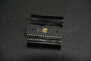
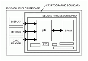
 Copy IC PIC16F886 Firmware
The Microchip PIC16F886 is a versatile 8-bit microcontroller widely used in various embedded applications, from consumer electronics and industrial automation to medical devices and automotive control systems. With its built-in EEPROM, Flash memory, 12-bit ADC, and enhanced capture/compare/PWM modules, the PIC16F886 is a favorite among engineers for projects that demand flexibility, compact size, and low power consumption.
However, the same qualities that make it ideal for integration also make it a challenge when it comes to firmware analysis or recovery—especially when the chip is locked, secured, or encrypted to prevent unauthorized access. At CIRCUIT ENGINEERING CO., LTD, we specialize in helping clients copy IC PIC16F886 firmware, including from protected or embedded systems.
Copy IC PIC16F886 Firmware and reprogramme the program into blank Microcontroller PIC16F886 which will provide the same functions as original MCU PIC16F886 after Crack MCU protective system;
High-Performance RISC CPU:
· Only 35 instructions to learn:
– All single-cycle instructions except branches
· Operating speed:
– DC – 20 MHz oscillator/clock input
– DC – 200 ns instruction cycle
· Interrupt capability

· 8-level deep hardware stack
· Direct, Indirect and Relative Addressing modes
Our expert team provides comprehensive services to copy, clone, or duplicate the firmware, binary, or heximal data from a secured PIC16F886 microcontroller. Whether you’re trying to restore a corrupted device, decode a legacy system, or unlock the original program for upgrades, we offer the technical capabilities and experience to assist you.
We work with:
- Encrypted and locked PIC16F886 devices
- Flash and EEPROM data extraction
- Heximal file recovery and source code reconstruction
- Memory mapping and firmware archive analysis
- Protected firmware decryption and reverse engineering
Using highly specialized techniques and proprietary hardware/software tools, our process enables the safe and accurate extraction of data, even from secured chips that most general programmers can’t access.
Special Microcontroller Features:
· Precision Internal Oscillator:
– Factory calibrated to ±1%
– Software selectable frequency range of 8 MHz to 31 kHz
– Software tunable
– Two-Speed Start-up mode
– Crystal fail detect for critical applications
– Clock mode switching during operation for power savings
· Power-Saving Sleep mode
· Wide operating voltage range (2.0V-5.5V)
· Industrial and Extended Temperature range
· Power-on Reset (POR)
· Power-up Timer (PWRT) and Oscillator Start-up Timer (OST)
· Brown-out Reset (BOR) with software control option
· Enhanced low-current Watchdog Timer (WDT) with on-chip oscillator (software selectable nominal 268 seconds with full prescaler) with software enable
· Multiplexed Master Clear with pull-up/input pin
· Programmable code protection
Understanding the structure and function of the PIC16F886 helps explain the demand for this service. The chip includes:
- 14KB of self-programmable Flash memory
- 368 bytes of SRAM
- 256 bytes of EEPROM
- Rich peripheral set (ADC, CCP, UART, SPI, I²C)
- Internal oscillator and watchdog timer
It’s commonly deployed in remote sensors, motor control, signal processing, and smart controller systems, where firmware updates or analysis might be required—especially in cases of hardware failure, lost documentation, or product redesign.
When a manufacturer fails to provide the original firmware, or when you’re working with a legacy system that’s no longer supported, copying the IC PIC16F886 firmware becomes a practical necessity. It may be the only way to restore full functionality or maintain operations in a production environment.

· High Endurance Flash/EEPROM cell:
– 100,000 write Flash endurance
– 1,000,000 write EEPROM endurance
– Flash/Data EEPROM retention: > 40 years
· Program memory Read/Write during run time
· In-Circuit Debugger (on board)
Low-Power Features:
· Standby Current:
– 50 nA @ 2.0V, typical
· Operating Current:
– 11 ìA @ 32 kHz, 2.0V, typical
– 220 ìA @ 4 MHz, 2.0V, typical
· Watchdog Timer Current:
– 1 ìA @ 2.0V, typical
Peripheral Features:
· 24/35 I/O pins with individual direction control
– High current source/sink for direct LED drive
– Interrupt-on-Change pin
– Individually programmable weak pull-ups
– Ultra Low-Power Wake-up (ULPWU)
· Analog Comparator module with:
While we offer the technical expertise to crack, hack, or decode locked firmware, our services are offered under strict confidentiality and within the boundaries of local laws. We support ethical reverse engineering, such as:
- System recovery
- Security research
- Legacy system maintenance
- Intellectual property retrieval for rightful owners
We do not engage in any services that violate the intellectual property rights of others.
– Two analog comparators
– Programmable on-chip voltage reference (CVREF) module (% of VDD)
– Fixed voltage reference (0.6V)
– Comparator inputs and outputs externally accessible
– SR Latch mode

– External Timer1 Gate (count enable)
· A/D Converter:
– 10-bit resolution and 11/14 channels
· Timer0: 8-bit timer/counter with 8-bit programmable prescaler
· Enhanced Timer1:
– 16-bit timer/counter with prescaler
– External Gate Input mode
– Dedicated low-power 32 kHz oscillator
· Timer2: 8-bit timer/counter with 8-bit period register, prescaler and postscaler
· Enhanced Capture, Compare, PWM+ module:
– 16-bit Capture, max. resolution 12.5 ns
– Compare, max. resolution 200 ns
– 10-bit PWM with 1, 2 or 4 output channels, programmable “dead time”, max. frequency 20 kHz
– PWM output steering control
· Capture, Compare, PWM module:
– 16-bit Capture, max. resolution 12.5 ns
– 16-bit Compare, max. resolution 200 ns
– 10-bit PWM, max. frequency 20 kHz
· Enhanced USART module:
– Supports RS-485, RS-232, and LIN 2.0
– Auto-Baud Detect
– Auto-Wake-Up on Start bit
· In-Circuit Serial ProgrammingTM (ICSPTM) via two pins
· Master Synchronous Serial Port (MSSP) module supporting 3-wire SPI (all 4 modes) and I2C™ Master and Slave Modes with I2C address mask
At CIRCUIT ENGINEERING CO., LTD, we combine technical precision, industry experience, and a deep understanding of embedded microcontroller architectures to deliver world-class firmware recovery solutions. If you’re struggling with a locked or damaged PIC16F886 and need to copy its internal data, we’re here to help.
Contact us today to learn more about how our services can help you copy IC PIC16F886 firmware, unlock valuable programs, and regain control of your embedded systems.
Attack IC MB90F598 Firmware
We can Break IC MB90F598 Firmware, please view the IC MB90F598 features below for your reference:
The MB90595/595G series with FULL-CAN*1 interface and FLASH ROM is especially designed for automotive and industrial applications. Its main features are two on board CAN Interfaces, which conform to V2.0 Part A and Part B, while supporting a very flexible message buffer scheme and so offering more functions than a normal full CAN approach when Attack IC.
The instruction set of F2MC-16LX CPU core inherits an AT architecture of the F2MC*2 family with additional instruction sets for high-level languages, extended addressing mode, enhanced multiplication/division instructions, and enhanced bit manipulation instructions. The microcontroller has a 32-bit accumulator for processing long word data after Attack IC.
The MB90595/595G series has peripheral resources of 8/10-bit A/D converters, UART (SCI), extended I/O serial interface, 8/16-bit PPG timer, I/O timer (input capture (ICU), output compare (OCU)) and stepping motor controller if Attack IC.
*1: Controller Area Network (CAN) – License of Robert Bosch GmbH
*2: F2MC stands for FUJITSU Flexible Microcontroller.
Clock
Embedded PLL clock multiplication circuit
Operating clock (PLL clock) can be selected from divided-by-2 of oscillation or one to four times the oscillation (at oscillation of 4 MHz, 4 MHz to 16 MHz) before Attack IC.
Minimum instruction execution time: 62.5 ns (operation at oscillation of 4 MHz, four times the oscillation clock, VCC of 5.0 V)
Instruction set to optimize controller applications
Rich data types (bit, byte, word, long word)
Rich addressing mode (23 types)
Enhanced signed multiplication/division instruction and RETI instruction functions after Attack IC
Enhanced precision calculation realized by the 32-bit accumulator
· Instruction set designed for high level language (C language) and multi-task operations
Adoption of system stack pointer
Enhanced pointer indirect instructions
Barrel shift instructions
· Program patch function (for two address pointers)
· Enhanced execution speed: 4-byte instruction queue
· Enhanced interrupt function: 8 levels, 34 factors when Attack IC
· Automatic data transmission function independent of CPU operation
Extended intelligent I/O service function (EI2OS): Up to 10 channels
· Embedded ROM size and types
Mask ROM: 128 Kbytes
Flash ROM: 128 Kbytes
Embedded RAM size: 4 Kbytes (MB90V595/595G : 6 Kbytes)
· Flash ROM
Supports automatic programming, Embedded Algorithm TM*
Write/Erase/Erase-Suspend/Resume commands after Attack IC
A flag indicating completion of the algorithm
Hard-wired reset vector available in order to point to a fixed boot sector
Erase can be performed on each block
Block protection with external programming voltage
· Low-power consumption (stand-by) mode
Sleep mode (mode in which CPU operating clock is stopped)
Stop mode (mode in which oscillation is stopped)
CPU intermittent operation mode
Hardware stand-by mode
· Process: 0.5 µm CMOS technology
· I/O port
General-purpose I/O ports: 78 ports
Push-pull output and Schmitt trigger input.
Programmable on each bit as I/O or signal for peripherals for Attack IC.
· Timer
Watchdog timer: 1 channel
8/16-bit PPG timer: 8/16-bit × 6 channels
16-bit re-load timer: 2 channels
· 16-bit I/O timer
Input capture: 4 channels
Output compare: 4 channels
· Extended I/O serial interface: 1 channel
· UART0
With full-duplex double buffer (8-bit length)
Clock asynchronized or clock synchronized (with start/stop bit) transmission can be selectively used.
UART1 (SCI)
With full-duplex double buffer (8-bit length)
Clock asynchronized or clock synchronized serial transmission (I/O extended transmission) can be selectively used if Attack IC.
· Stepping motor controller (4 channels)
· External interrupt circuit (8 channels)
A module for starting an extended intelligent I/O service (EI2OS) and generating an external interrupt which is triggered by an external input.
· Delayed interrupt generation module: Generates an interrupt request for switching tasks.
· 8/10-bit A/D converter (8 channels)
8/10-bit resolution can be selectively used.
Starting by an external trigger input.
· FULL-CAN interface: 1 channel
Conforming to Version 2.0 Part A and Part B
Flexible message buffering (mailbox and FIFO buffering can be mixed) after Attack IC
· 18-bit Time-base counter
· External bus interface: Maximum address space 16 Mbytes
*: Embedded Algorithm is a trademark of Advanced Micro Devices Inc.
Break Chip PIC16F716 Heximal
The PIC16F716 is a compact yet powerful 8-bit microcontroller (MCU) developed by Microchip Technology, widely deployed in industrial control, home automation, and sensor-driven applications. Designed with cost efficiency and simplicity in mind, this MCU features a Flash-based program memory, internal EEPROM, analog comparators, and an integrated oscillator—all in a compact 18-pin package. While ideal for embedded systems, its protected firmware often presents challenges when data recovery or firmware duplication is necessary.

At CIRCUIT ENGINEERING CO., LTD, we specialize in offering advanced reverse engineering services to break chip PIC16F716 heximal files. This includes the ability to crack, decode, and decrypt protected program memory and EEPROM data from the chip, even when the device is secured or locked using Microchip’s code protection mechanisms.
Break Chip PIC16F716 and extract Heximal out from MCU PIC16F716 flash memory, the security fuse bit of Microcontroller PIC16F716 can be removed or disable for the original MCU PIC16F716;
When clients need access to the firmware inside the PIC16F716, standard reading tools often fail due to built-in encryption and lock bits. Our team uses proprietary techniques and hardware-level exploit strategies to unlock and copy the embedded binary or heximal file from Flash or EEPROM memory. Once recovered, the data can be converted into a source code archive for analysis, debugging, or replication.

Our services cover a full range of tasks, including:
- Crack and unlock code-protected memory areas
- Restore lost or corrupted firmware from embedded devices
- Duplicate or clone firmware for hardware replacement or scale-up production
- Decrypt and decode the program file into human-readable logic
- Generate commented disassemblies or higher-level reconstructions from raw memory dumps
Microcontroller Core Features:
· High-performance RISC CPU
· Only 35 single-word instructions to learn
– All single-cycle instructions except for
program branches which are two-cycle
· Operating speed: DC – 20 MHz clock input
DC – 200 ns instruction cycle
· Interrupt capability (up to 7 internal/external interrupt sources)
· 8-level deep hardware stack
· Direct, Indirect and Relative Addressing modes
Special Microcontroller Features:
· Power-on Reset (POR)
· Power-up Timer (PWRT) and
Oscillator Start-up Timer (OST)
· Watchdog Timer (WDT) with its own on-chip RC
oscillator for reliable operation
· Dual level Brown-out Reset circuitry
– 2.5 VBOR (Typical)
– 4.0 VBOR (Typical)
· Programmable code protection
· Power-Saving Sleep mode
· Selectable oscillator options
· Fully static design
· In-Circuit Serial Programming (ICSP™)
CMOS Technology:
· Wide operating voltage range:
– Industrial: 2.0V to 5.5V
– Extended: 3.0V to 5.5V
· High Sink/Source Current 25/25 mA
· Wide temperature range:
– Industrial: -40°C to 85°C
– Extended: -40°C to 125°C
Low-Power Features:
· Standby Current:
– 100 nA @ 2.0V, typical
· Operating Current:
– 14 ìA @ 32 kHz, 2.0V, typical
– 120 ìA @ 1 MHz, 2.0V, typical
– 1 ìA @ 2.0V, typical
· Timer1 Oscillator Current:
– 3.0 ìA @ 32 kHz, 2.0V, typical
The PIC16F716 is tailored for real-time control in resource-constrained environments. With features like:

- 2K words of Flash program memory
- 128 bytes of EEPROM
- 128 bytes of RAM
- Internal 4 MHz oscillator
- Multiple analog comparators
…it is often used in low-cost embedded control applications such as:
- Home appliance control boards
- Power supplies and battery charging circuits
- Environmental monitoring and sensor hubs
- Automotive lighting and low-level control logic
This makes the PIC16F716 a prime candidate for firmware copying, especially when systems are no longer supported or require restoration after hardware failure.
Why Choose Our Reverse Engineering Solutions?
Many businesses, repair engineers, or developers face the urgent need to recover firmware from a locked, secured, or encrypted PIC16F716 chip. That’s where our deep expertise in firmware disassembly, memory analysis, and protected data extraction becomes invaluable.
We maintain strict confidentiality and legal compliance while providing efficient, low-risk firmware recovery services. Whether you’ve lost the original source files or need to duplicate a critical control board, we can extract, decrypt, and return the full heximal program archive to you in a readable format.
Peripheral Features:
· Timer0: 8-bit timer/counter with 8-bit prescaler can be incremented during Sleep via external crystal/clock
· Timer2: 8-bit timer/counter with 8-bit period register, prescaler and postscaler
· Enhanced Capture, Compare, PWM module:
– Capture is 16-bit, max. resolution is 12.5 ns
– Compare is 16-bit, max. resolution is 200 ns
– PWM maximum resolution is 10-bit
– Enhanced PWM:
– Single, Half-Bridge and Full-Bridge modes
– Digitally programmable dead-band delay
– Auto-shutdown/restart
· 8-bit multi-channel Analog-to-Digital Converter
· 13 I/O pins with individual direction control
· Programmable weak pull-ups on PORTB
Our “break chip PIC16F716 heximal” service empowers you to regain control over your embedded systems by opening up protected memory, restoring lost firmware, and enabling you to clone or copy the program data for future use. Don’t let a locked microcontroller stop your operations—contact [Your Company Name] today for professional, discrete, and highly accurate firmware recovery services tailored to your needs.
Break Microcontroller MC68376BACAB25 Program
We can Break Microcontroller MC68376BACAB25 Program, please view below Microcontroller MC68376BACAB25 features for your reference:
The MC68336 and the MC68376 are highly-integrated 32-bit microcontrollers, combining high-performance data manipulation capabilities with powerful peripheral subsystems.
MC68300 microcontrollers are built up from standard modules that interface through a common intermodule bus (IMB). Standardization facilitates rapid development of devices tailored for specific applications when Break Microcontroller.
The MC68336 incorporates a 32-bit CPU (CPU32), a system integration module (SIM), a time processor unit (TPU), a configurable timer module (CTM4), a queued serial module (QSM), a 10-bit queued analog-to-digital converter module (QADC), a 3.5-Kbyte TPU emulation RAM module (TPURAM), and a 4-Kbyte standby RAM module (SRAM) if Break Microcontroller.
The MC68376 includes all of the aforementioned modules, plus a CAN 2.0B protocol controller module (TouCAN™) and an 8-Kbyte masked ROM (MRM).
The MC68336/376 can either synthesize the system clock signal from a fast reference or use an external clock input directly after Break Microcontroller. Operation with a 4.194 MHz reference frequency is standard. The maximum system clock speed is 20.97 MHz. System hardware and software allow changes in clock rate during operation. Because MCU operation is fully static, register and memory contents are not affected by clock rate changes before Break Microcontroller.
High-density complementary metal-oxide semiconductor (HCMOS) architecture makes the basic power consumption of the MCU low. Power consumption can be minimized by stopping the system clock. The CPU32 instruction set includes a low-power stop (LPSTOP) instruction that efficiently implements this capability after Break Microcontroller.
Documentation for the Modular Microcontroller Family follows the modular construction of the devices in the product line. Each microcontroller has a comprehensive user’s manual that provides sufficient information for normal operation of the device before Break Microcontroller.
The user’s manual is supplemented by module reference manuals that provide detailed information about module operation and applications. Refer to Motorola publication Advanced Microcontroller Unit (AMCU) Literature (BR1116/D) for a complete listing of documentation when Break IC.
Break MCU MC68HC11F1CFN3 Heximal
The MC68HC11F1CFN3, a legacy 8-bit microcontroller from Freescale (formerly Motorola), has long served in automotive, industrial, and consumer electronics applications. Known for its robust performance and integrated features—including on-chip A/D converters, serial communication interfaces, and internal EEPROM—it remains embedded in critical systems even today. However, its protected memory, often secured by hardware security bits, presents a significant challenge when attempting to extract or modify the firmware for maintenance, analysis, or system upgrade.

At CIRCUIT ENGINEERING CO.,LTD, we specialize in professional microcontroller reverse engineering services. Our expertise allows us to break MCU MC68HC11F1CFN3 heximal, enabling clients to access and restore the original binary, heximal, or source code from these highly secured, locked microcontrollers.
Break MCU MC68HC11F1CFN3 tamper resistance system and read heximal file out from Microcontroller MC68HC11F1, status of Microprocessor will be reset from locked to unlocked one;
Our process begins by carefully analyzing the device’s flash and EEPROM architecture. Using non-invasive and semi-invasive methods, we can crack, hack, and unlock the memory content without damaging the chip—preserving its functionality while retrieving critical data.
We extract the heximal file from the target MCU, decode the firmware, and, where necessary, decrypt encrypted sections. From there, we can help you clone or duplicate the program, convert it to a more accessible archive, or even reconstruct it into human-readable source code through disassembly or decompilation techniques.

Whether you need to copy a protected system for diagnostics or replicate functionality in a modernized platform, our service enables complete access to what was once considered inaccessible.
Features
· MC68HC11 CPU
· Power Saving STOP and WAIT Modes
· 4 Kbytes of On-Chip ROM
· 192 Bytes of On-Chip RAM (All Saved During Standby)
· 16-Bit Timer System
— 3 Input Capture (IC) Channels
— 4 Output Compare (OC) Channels
— One IC or OC Channel (Software Selectable)
· 8-Bit Pulse Accumulator
· Real-Time Interrupt Circuit
· Computer Operating Properly (COP) Watchdog System
· Synchronous Serial Peripheral Interface (SPI)
· Asynchronous Nonreturn to Zero (NRZ) Serial Communications Interface (SCI)
· 26 Input/Output (I/O) Pins
— 16 Bidirectional I/O Pins
— 3 Input Only Pins
— 3 Output Only Pins (One Output Only Pin in the 40-Pin Package)
· Available in a 44-Pin Plastic Leaded Chip Carrier (PLCC) and 40-Pin Dual In-Line Package (DIP) 2.1 VDD, VSS, and EVSS
Power is supplied to the MCU through VDD and VSS. VSS is the power supply, and VSS is ground. EVSS, available on the 44-pin PLCC, is an additional ground pin that must be grounded with VSS. The MCU operates from a single 5-volt (nominal) power supply. Very fast signal transitions occur on the MCU pins. The short rise and fall times place high, short duration current demands on the power supply. To prevent noise problems, provide good power supply bypassing at the MCU. Also, use bypass capacitors that have good high-frequency characteristics and situate them as close to the MCU as possible. Bypass requirements vary, depending on how heavily the MCU pins are loaded.

Hardware-Specific Expertise: We’re deeply familiar with the quirks and protections of the Freescale MC68HC11F1CFN3 and similar legacy devices. This means faster, safer results.
Precision and Confidentiality: We maintain strict protocols for secure data handling. All recovered firmware and files are handled with confidentiality.
End-to-End Support: We don’t just deliver raw data—we assist with interpretation, conversion, and integration into your current systems.
No Damage Guarantee: Our methods aim to preserve chip function post-extraction whenever possible, ideal for reuse or archival.
2.2 Reset (RESET)
An active low bidirectional control signal, RESET, acts as an input to initialize the MCU to a known startup state. It also acts as an open-drain output to indicate that an internal failure has been detected in either the clock monitor or COP watchdog circuit. The CPU distinguishes between internal and external reset conditions by sensing whether the reset pin rises to a logic one in less than two E-clock cycles after a reset has occurred. It is not advisable to connect an external resistor-capacitor (RC) power-up delay circuit to the reset pin of M68HC11 devices because the circuit charge time 2.3 Crystal Driver and External Clock Input (XTAL, EXTAL)
The MC68HC11F1CFN3 remains in use today due to its proven reliability in automotive control units, instrument clusters, industrial automation controllers, and legacy consumer electronics. With on-board RAM, internal EEPROM, and a flexible I/O architecture, it’s built to handle low-latency control tasks in embedded systems.
One standout feature is its bootstrap ROM, which can be leveraged for in-circuit programming or diagnostics. However, many of these features are locked down with hardware-level protection to prevent tampering or duplication—a hurdle we help you overcome.
These two pins provide the interface for either a crystal or a CMOS compatible clock to control the internal clock generator circuitry. The frequency applied to these pins is four times higher than the desired E-clock rate.
The XTAL pin is normally left unterminated when an external CMOS compatible clock input is connected to the EXTAL pin. However, a 10 kΩ to 100 kΩ load resistor connected from XTAL to ground can be used to reduce RFI noise emission. The XTAL output is normally intended to drive only a crystal. The XTAL output can be buffered with a high impedance buffer, or it can be used to drive the EXTAL input of another M68HC11.
Whether you’re tasked with maintaining a fleet of legacy control systems, duplicating a protected embedded environment, or auditing a third-party solution, our ability to break MCU MC68HC11F1CFN3 heximal and recover its firmware is your path forward. Our service is built for professionals who demand access, clarity, and reliability from even the most secured and encrypted systems.
Contact us today to learn how we can help you unlock, decode, and restore the full functionality of your Freescale MC68HC11F1CFN3-based systems.
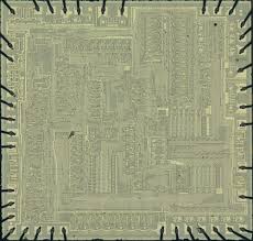
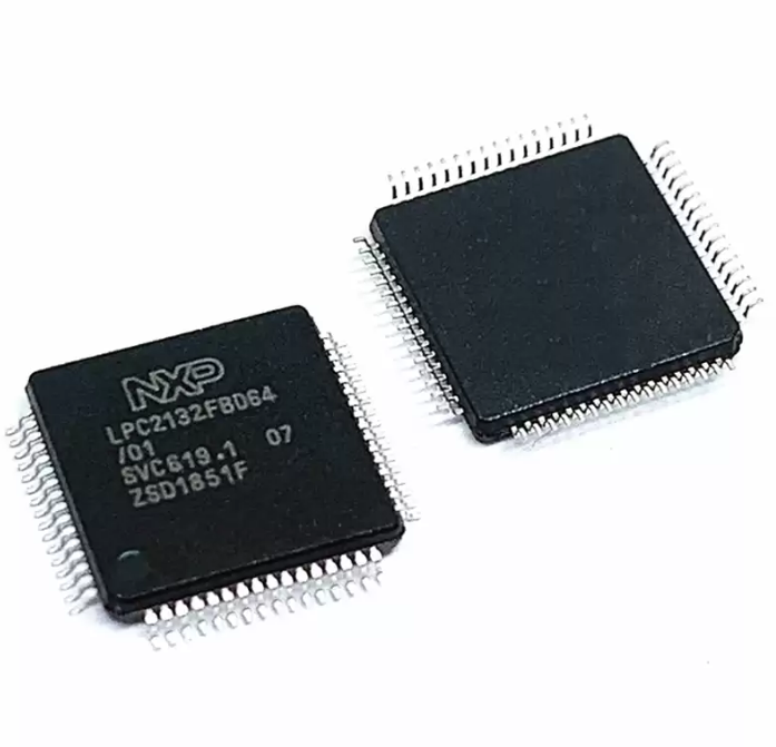
Break IC LPC2132FBD64 Firmware
In the field of embedded electronics, the LPC2132FBD64 microcontroller—based on the ARM7TDMI-S core—is widely used in applications ranging from industrial control to medical devices and consumer electronics. With its integrated 512KB Flash memory, rich peripheral set, and advanced features, it has become a reliable choice for secure embedded system design. However, its protected and encrypted firmware often poses a significant obstacle when users need to regain access to a device’s functionality or replicate legacy systems. That’s where we come in.
At CIRCUIT ENGINEERING CO.,LTD, we specialize in providing professional services to break IC LPC2132FBD64 firmware, allowing end users and engineers to unlock, copy, and restore the internal code of secured and locked microcontrollers. Whether it’s for product repair, legacy system recovery, or R&D, our solutions are designed to disable fuse bits, bypass read protection, and extract data securely and confidentially.
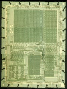
Break IC LPC2132FBD64 program memory and readout firmware from Microcontroller LPC2132FBD64, focus ion beam technique will be applied to reset the status of MCU LPC2132FBD64 from locked to unlocked one;
The LPC2132 microcontrollers are based on a 32/16 bit ARM7TDMI-S CPU with real-time emulation and embedded trace support, that combines the microcontroller with 32 kB, 64 kB, 128 kB, 256 kB and 512 kB of embedded high speed Flash memory.
Manufacturers often implement security features in microcontrollers like the LPC2132FBD64 to lock the firmware and prevent unauthorized access. While this protects intellectual property, it can become problematic for legitimate users when the original developer is unavailable, the firmware is lost, or a system needs modification. The chip’s security bits and fuse protections are intentionally designed to prevent reading of the flash, EEPROM, or memory archive, even with direct access to the device.
Using proprietary techniques and custom hardware interfaces, our team can carefully crack, decode, and read out the binary or heximal firmware of the LPC2132FBD64 without damaging the hardware. We also offer advanced decryption and disassembly services to convert the extracted data into readable source code or program files, enabling full analysis, reuse, or migration to other platforms.
The LPC2132FBD64 is valued for its compact 64-pin LQFP package and high-speed 60MHz CPU operation. It features two 10-bit ADCs, multiple UARTs, SPI/I2C interfaces, PWM channels, and USB 1.1 full-speed support—making it a powerful and versatile microcontroller in embedded system design. These rich peripherals are often deeply tied into the firmware, meaning that gaining access to the code is crucial for re-implementation, debugging, or custom development.
A 128-bit wide memory interface and a unique accelerator architecture enable 32-bit code execution at maximum clock rate. For critical code size applications, the alternative 16-bit Thumb mode reduces code by more than 30 % with minimal performance penalty after Copying IC PIC16F84A binary.
Our Complete Service Offering
- Firmware extraction from locked LPC2132FBD64 ICs
- Fuse bit disablement and read protection bypass
- Binary and heximal data recovery
- Conversion to C-style source code or annotated assembly
- Cloning and duplication for system replication
- Secure handling and confidential data management
Our services are trusted by electronics repair centers, product manufacturers, forensic investigators, and reverse engineering specialists. We treat each project with strict confidentiality and provide documentation of the process upon request.
Due to their tiny size and low power consumption, these microcontrollers are ideal for applications where miniaturization is a key requirement, such as access control and point-of-sale. With a wide range of serial communications interfaces and on-chip SRAM options of 8/16/32 kB, they are very well suited for communication gateways and protocol converters, soft modems, voice recognition and low end imaging, providing both large buffer size and high processing power. Various 32-bit timers, single or dual 10-bit 8 channel ADC(s), 10-bit DAC, PWM channels and 47 GPIO lines with up to nine edge or level sensitive external interrupt pins make these microcontrollers particularly suitable for industrial control and medical systems after attacking C8051F530 firmware.
16/32-bit ARM7TDMI-S microcontroller in a tiny LQFP64 package.
8/16/32 kB of on-chip static RAM and 32/64/128/256/512 kB of on-chip Flash program memory. 128 bit wide interface/accelerator enables high speed 60 MHz operation. In-System/In-Application Programming (ISP/IAP) via on-chip boot-loader software.
Single Flash sector or full chip erase in 400 ms and programming of 256 bytes in 1 ms. EmbeddedICE RT and Embedded Trace interfaces offer real-time debugging with the on-chip RealMonitor software and high speed tracing of instruction execution.
One (LPC2132) or two (LPC2134/36/38) 8 channel 10-bit A/D converters provides a total of up to 16 analog inputs, with conversion times as low as 2.44 µs per channel. Single 10-bit D/A converter provides variable analog output (LPC2132). Two 32-bit timers/external event counters (with four capture and four compare channels each), PWM unit (six outputs) and watchdog after attack microcontroller PIC16C63A heximal.
Low power Real-time clock with independent power and dedicated 32 kHz clock input.
Multiple serial interfaces including two UARTs (16C550), two Fast I2C-bus (400 kbit/s),
SPI and SSP with buffering and variable data length capabilities.
Vectored interrupt controller with configurable priorities and vector addresses.
Up to 47 5 V tolerant general purpose I/O pins in tiny LQFP64 package.
Up to nine edge or level sensitive external interrupt pins available.
60 MHz maximum CPU clock available from programmable on-chip PLL with settling time of 100 µs.
On-chip integrated oscillator operates with external crystal in range of 1 MHz to
30 MHz and with external oscillator up to 50 MHz.
Power saving modes include Idle and Power-down
Individual enable/disable of peripheral functions as well as peripheral clock scaling down for additional power optimization.
Processor wake-up from Power-down mode via external interrupt or BOD.
Single power supply chip with POR and BOD circuits:
CPU operating voltage range of 3.0 V to 3.6 V (3.3 V ± 10 %) with 5 V tolerant I/O pads.
Recover Chip MC68HC11A0FN3 Binary
The Motorola/Freescale MC68HC11A0FN3 is a powerful 8-bit microcontroller widely used in industrial control, automotive electronics, robotics, and legacy embedded systems. Known for its on-chip EEPROM, robust flash memory, and versatile I/O capabilities, this chip has long served as the backbone of many secure and high-performance applications. However, its protected architecture, often with fuse-bit security or memory lockout mechanisms, makes it extremely difficult for users to access or recover the internal binary or firmware once programmed.

We specialize in advanced microcontroller security bypassing. Our premium service to recover chip MC68HC11A0FN3 binary is tailored for professionals needing access to original firmware, source code, or heximal data stored inside this secured embedded device.
Recover Chip MC68HC11A0FN3 Binary from Microcontroller MC68HC11A0FN3 program memory, unlock microprocessor MC68HC11A0FN3 security fuse bit and extract heximal out from memory;
The MC68HC11A0FN3 is frequently found in applications where the firmware is locked, encrypted, or protected to safeguard intellectual property. But what happens when original files are lost, the system malfunctions, or a firmware update is required? Most off-the-shelf tools are helpless when faced with the chip’s security fuses and protected memory layout.
This is where our team steps in—with precision and discretion. We offer the ability to crack, hack, or unlock the internal memory of secured MCUs like the MC68HC11A0FN3. By applying advanced microprobing, signal analysis, or fuse-disabling methodologies, we can decrypt, decode, and open the locked memory region to retrieve the original program, archive, or data file.
· Power Saving STOP and WAIT Modes
· 4 Kbytes of On-Chip ROM
· 192 Bytes of On-Chip RAM (All Saved During Standby)
· 16-Bit Timer System
— 3 Input Capture (IC) Channels
— 4 Output Compare (OC) Channels
— One IC or OC Channel (Software Selectable)
Our MC68HC11A0FN3 reverse engineering and data extraction services include:

- Fuse Bit Disabling: We employ non-destructive or minimally invasive techniques to disable fuse bits, giving access to protected flash, EEPROM, and firmware memory.
- Binary Extraction: We can copy, clone, or duplicate the original binary or heximal data, even from secured or damaged chips.
- Conversion to Source Code: The recovered data can be disassembled and, in many cases, translated back to readable source code for audit, debugging, or redevelopment purposes.
- Firmware Recovery: Whether due to data loss, hardware failure, or lack of documentation, we can restore your device’s original firmware for continued operation or migration to modern hardware.
· 8-Bit Pulse Accumulator
· Real-Time Interrupt Circuit
· Computer Operating Properly (COP) Watchdog System
· Synchronous Serial Peripheral Interface (SPI)
· Asynchronous Nonreturn to Zero (NRZ) Serial Communications Interface (SCI)
· 26 Input/Output (I/O) Pins
— 16 Bidirectional I/O Pins
— 3 Input Only Pins
— 3 Output Only Pins (One Output Only Pin in the 40-Pin Package)
· Available in a 44-Pin Plastic Leaded Chip Carrier (PLCC) and 40-Pin Dual In-Line Package (DIP)
2.1 VDD, VSS, and EVSS
This chip is not just a legacy device; it remains embedded in critical systems such as:
- Automotive ECUs: Engine control, ABS, and dashboard systems.
- Industrial Automation: Programmable controllers, safety relays, and process monitors.
- Medical Devices: Legacy diagnostic machines and custom sensors.
- Aerospace Systems: Avionic support tools and aircraft diagnostics.
Many of these systems still rely on the original code running on the MC68HC11A0FN3. Without proper access, maintaining or upgrading them becomes nearly impossible.
Power is supplied to the MCU through VDD and VSS. VSS is the power supply, and VSS is ground. EVSS, available on the 44-pin PLCC, is an additional ground pin that must be grounded with VSS. The MCU operates from a single 5-volt (nominal) power supply before MCU PIC32MX440F512H binary copying. Very fast signal transitions occur on the MCU pins.
The short rise and fall times place high, short duration current demands on the power supply. To prevent noise problems, provide good power supply bypassing at the MCU. Also, use bypass capacitors that have good high-frequency characteristics and situate them as close to the MCU as possible. Bypass requirements vary, depending on how heavily the MCU pins are loaded.

2.2 Reset (RESET)
An active low bidirectional control signal, RESET, acts as an input to initialize the MCU to a known startup state. It also acts as an open-drain output to indicate that an internal failure has been detected in either the clock monitor or COP watchdog circuit. The CPU distinguishes between internal and external reset conditions by sensing whether the reset pin rises to a logic one in less than two E-clock cycles after a reset has occurred. It is not advisable to connect an external resistor-capacitor (RC) power-up delay circuit to the reset pin of M68HC11 devices because the circuit charge time.
2.3 Crystal Driver and External Clock Input (XTAL, EXTAL)
These two pins provide the interface for either a crystal or a CMOS compatible clock to control the internal clock generator circuitry. The frequency applied to these pins is four times higher than the desired E-clock rate after Recover MCU PIC16F913 bin.
The XTAL pin is normally left unterminated when an external CMOS compatible clock input is connected to the EXTAL pin. However, a 10 kΩ to 100 kΩ load resistor connected from XTAL to ground can be used to reduce RFI noise emission. The XTAL output is normally intended to drive only a crystal. The XTAL output can be buffered with a high impedance buffer, or it can be used to drive the EXTAL input of another M68HC11.
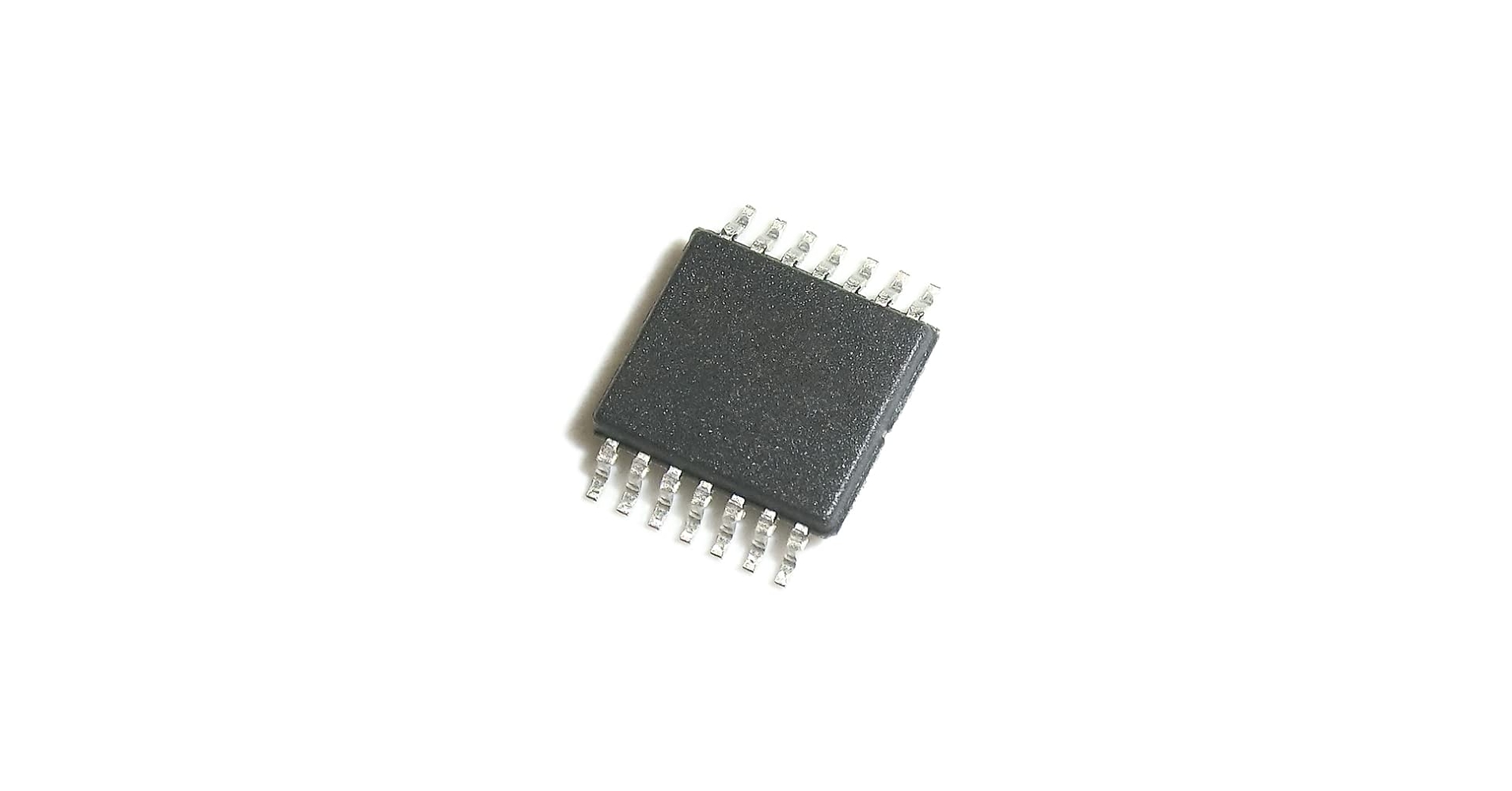
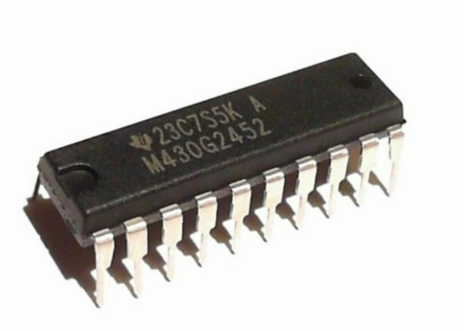
Recover Microcontroller 430G2452 Heximal
Our specialized service enables you to recover Microcontroller 430G2452 heximal code, helping you bypass locked or encrypted firmware and extract essential data. Whether your objective is to restore a legacy system, copy a failed firmware image, or clone a working configuration for backup or migration, our team provides safe and reliable solutions.
We employ advanced hardware-assisted techniques to crack and decode the protection mechanisms of the MCU. This includes overcoming secured fuse bits, accessing locked flash memory, and retrieving data from both program memory and EEPROM-like segments. Once unlocked, the extracted binary or heximal firmware is processed into readable source code or annotated assembly, depending on your need for analysis, porting, or documentation.
Recover Microcontroller 430G2452 Heximal out from MCU MSP430G2452 is a process start from Crack MCU MSP430G2452 protective system and disable its security fuse bit by focus ion beam, then copy the code fro new microcontroller;
FEATURES
Low Supply Voltage Range: 1.8 V to 3.6 V Ultra-Low Power Consumption
– Active Mode: 220 µA at 1 MHz, 2.2 V
– Standby Mode: 0.5 µA
– Off Mode (RAM Retention): 0.1 µA
Five Power-Saving Modes Ultra-Fast Wake-Up From Standby Mode in Less Than 1 µs 16-Bit RISC Architecture, 62.5-ns Instruction Cycle Time.
Basic Clock Module Configurations
– Internal Frequencies up to 16 MHz With
Four Calibrated Frequencies
– Internal Very-Low-Power Low-Frequency (LF) Oscillator
– 32-kHz Crystal
– External Digital Clock Source
One 16-Bit Timer_A With Three Capture/Compare Registers Up to 16 Touch-Sense Enabled I/O Pins
Universal Serial Interface (USI) Supporting SPI and I2C 10-Bit 200-ksps Analog-to-Digital (A/D)
Converter With Internal Reference, Sample-and-Hold, and Autoscan (MSP430G2x52 Only) On-Chip Comparator for Analog Brownout Detector Serial Onboard Programming, No External Programming Voltage Needed, Programmable Code Protection by Security Fuse On-Chip Emulation Logic With Spy-Bi-Wire Interface Family Members are Summarized:
Package Options
– TSSOP: 14 Pin, 20 Pin
– PDIP: 20 Pin
– QFN: 16 Pin
For Complete Module Descriptions, See the MSP430x2xx Family User’s Guide (SLAU144)
DESCRIPTION
The Texas Instruments MSP430™ family of ultra-low-power microcontrollers consist of several devices featuring different sets of peripherals targeted for various applications. The architecture, combined with five low-power modes, is optimized to achieve extended battery life in portable measurement applications.
The device features a powerful 16-bit RISC CPU, 16-bit registers, and constant generators that contribute to maximum code efficiency. The digitally controlled oscillator (DCO) allows wake-up from low-power modes to active mode in less than 1 µs.
The MSP430G2x52 and MSP430G2x12 series of microcontrollers are ultra-low-power mixed signal microcontrollers with built-in 16-bit timers, and up to 16 I/O touch sense enabled pins and built-in communication capability using the universal serial communication interface and have a versatile analog comparator.
The MSP430G2x52 series have a 10-bit A/D converter. For configuration details see Table 1. Typical applications include low-cost sensor systems that capture analog signals, convert them to digital values, and then process the data for display or for transmission to a host system when attacking Microcontrolle ST62T15C6 firmware memory.
Core Services Offered:
- Fuse Bit Bypass: Disable fuse protection to allow memory access.
- Firmware Extraction: Retrieve full program memory, eeprom, and configuration data.
- Binary/Heximal to Source: Convert raw memory dumps into readable C-like code or reconstruct assembly.
- Data Recovery: Recover lost or corrupted firmware from damaged or bricked units.
- System Cloning: Create functionally identical duplicates for hardware migration or replication.
- Security Testing: Evaluate your system’s resilience by simulating a penetration attempt into encrypted or protected MCUs.
Why Choose Us?
- Deep Expertise in MSP430 Architecture: We understand the protection mechanisms, memory layout, and debug interface of the 430G2452 inside-out.
- Confidential & Legal Compliance: Your data and intellectual property are handled securely, with strict confidentiality measures.
- Custom Reporting: We provide optional documentation outlining the structure, functions, and memory map of recovered program files or archives.
- Flexible Delivery: Whether you need a raw binary, disassembled listing, or decompiled source code, we deliver what fits your workflow.
Application Scenarios
MSP430G2452 is often deployed in wearable medical sensors, remote controls, industrial sensors, battery-operated meters, and consumer electronics. When the original source code is lost or the firmware becomes locked, our service ensures your product lifecycle doesn’t come to a halt. Recovering firmware from protected chips isn’t just about duplication—it’s about preserving investment, minimizing downtime, and enabling further innovation.
Recover MCU PIC18F2520 Binary
In the world of embedded systems, the MCU PIC18F2520 stands out as a powerful and reliable microcontroller widely used in automotive electronics, industrial automation, home appliances, and communication equipment. Its popularity stems from its robust performance, built-in EEPROM, and extensive I/O capabilities, making it ideal for real-time applications. However, what makes it secure for manufacturers also makes it difficult for end users to access or modify its internal firmware, especially when the chip is protected with fuse bits.

At CIRCUIT ENGINEERING CO., LTD, we offer advanced services to Recover MCU PIC18F2520 Binary, helping clients copy, clone, or duplicate the original program stored in the flash memory or EEPROM, even if the device is locked, encrypted, or secured. Whether you’ve lost the original source code, need to restore malfunctioning devices, or want to analyze existing data, we can help you unlock the chip and decode its contents with precision.
Recover MCU PIC18F2520 Binary from Microcontroller PIC18F2520 program memory, reset the security fuse bit inside the protective system from locked to unlocked one by Crack MCU PIC18F2520;
Many PIC18F2520 chips are shipped with fuse bits enabled, which disable standard read-out functions and make it nearly impossible to access the internal heximal firmware using traditional programmers. These protections are designed to prevent reverse engineering or unauthorized duplication, but they also pose significant challenges for legitimate developers and technicians needing to recover, modify, or migrate firmware to new hardware.

Our team is equipped with the tools and expertise required to crack these protections and bypass the fuse bits, allowing full access to the locked binary file. This process may involve decoding the archive stored in memory, reading from protected flash, or extracting the program data via low-level hardware or side-channel techniques.
Power Management Features:
Peripheral Highlights (Continued):
Run: CPU on, Peripherals on
Idle: CPU off, Peripherals on
Sleep: CPU off, Peripherals off
Ultra Low 50nA Input Leakage
Run mode Currents Down to 11 ìA Typical
Idle mode Currents Down to 2.5 ìA Typical
Sleep mode Current Down to 100 nA Typical
Timer1 Oscillator: 900 nA, 32 kHz, 2V
Watchdog Timer: 1.4 ìA, 2V Typical
Two-Speed Oscillator Start-up
Once the protected firmware is successfully extracted, we offer further services to convert the binary into human-readable formats. Our decryption pipeline includes transforming heximal data into assembly code, and in many cases, we can decompile the binary into partial or complete C source code.
This enables you to:
Restore damaged or bricked devices where firmware is corrupted or lost
Troubleshoot errors and bugs in legacy systems
Upgrade or modify existing embedded applications
Clone systems for mass production when the original code is unavailable
Perform security audits or validate device integrity
· Master Synchronous Serial Port (MSSP) module
Supporting 3-Wire SPI (all 4 modes) and I2C™
Master and Slave modes
· Enhanced Addressable USART module:
– Supports RS-485, RS-232 and LIN/J2602
– RS-232 operation using internal oscillator block (no external crystal required)
– Auto-wake-up on Start bit
– Auto-Baud Detect
· 10-Bit, up to 13-Channel Analog-to-Digital (A/D)

Flexible Oscillator Structure:
· Four Crystal modes, up to 40 MHz
· 4x Phase Lock Loop (PLL) – Available for Crystal and Internal Oscillators
· Two External RC modes, up to 4 MHz
· Two External Clock modes, up to 40 MHz
· Internal Oscillator Block:
– Fast wake from Sleep and Idle, 1 ìs typical
– 8 use-selectable frequencies, from 31 kHz to 8 MHz
– Provides a complete range of clock speeds from 31 kHz to 32 MHz when used with PLL
– User-tunable to compensate for frequency drift
· Secondary Oscillator using Timer1 @ 32 kHz
· Fail-Safe Clock Monitor:
– Allows for safe shutdown if peripheral clock stops
Peripheral Highlights:
Converter module:
– Auto-acquisition capability
– Conversion available during Sleep
· Dual Analog Comparators with Input Multiplexing
· Programmable 16-Level High/Low-Voltage
Detection (HLVD) module:
– Supports interrupt on High/Low-Voltage Detection
Special Microcontroller Features:
· C Compiler Optimized Architecture:
– Optional extended instruction set designed to
optimize re-entrant code
· 100,000 Erase/Write Cycle Enhanced Flash
Program Memory Typical
· 1,000,000 Erase/Write Cycle Data EEPROM
Memory Typical
· Flash/Data EEPROM Retention: 100 Years Typical
· Self-Programmable under Software Control
High-Current Sink/Source 25 mA/25 mA
Three Programmable External Interrupts
Four Input Change Interrupts
Up to 2 Capture/Compare/PWM (CCP) modules,
· Priority Levels for Interrupts
· 8 x 8 Single-Cycle Hardware Multiplier
· Extended Watchdog Timer (WDT):
– Programmable period from 4 ms to 131s one with Auto-Shutdown (28-pin devices)
· Enhanced Capture/Compare/PWM (ECCP) module (40/44-pin devices only):
– One, two or four PWM outputs
– Selectable polarity
– Programmable dead time
– Auto-shutdown and auto-restart
· Single-Supply 5V In-Circuit Serial
Programming™ (ICSP™) via Two Pins
· In-Circuit Debug (ICD) via Two Pins
· Wide Operating Voltage Range: 2.0V to 5.5V
· Programmable Brown-out Reset (BOR) with
Software Enable Option
The PIC18F2520 is used in a wide range of commercial and industrial systems. From automotive ECUs to industrial sensors and consumer electronics, our clients often need to open or duplicate protected firmware to ensure service continuity, compatibility, or quality control. When the manufacturer is no longer available or documentation is missing, we help recover the MCU PIC18F2520 binary, ensuring your hardware remains viable for years to come.
Let us help you take control of your embedded system’s firmware. Contact us to learn how we can unlock, decrypt, and restore what others consider impossible.
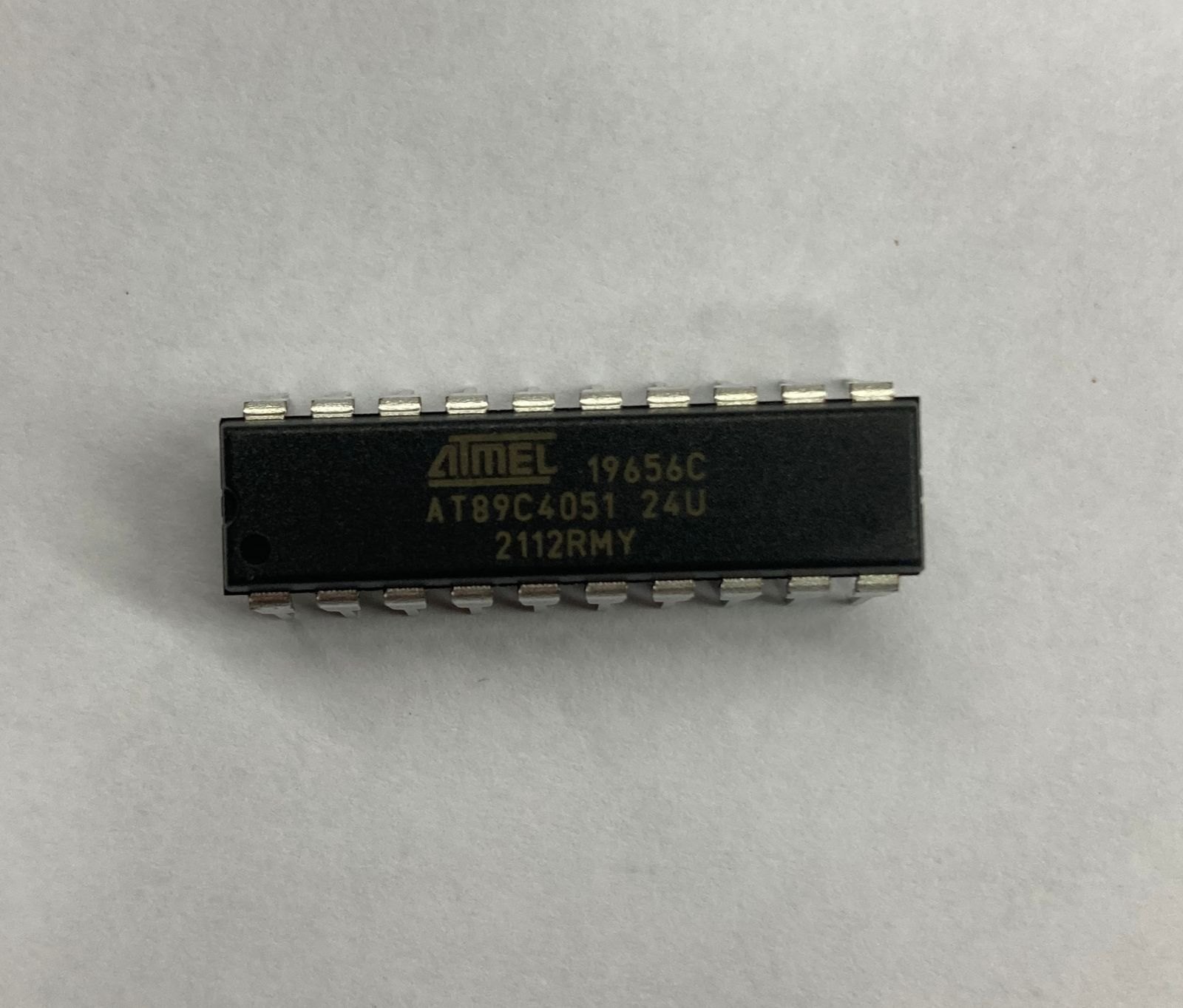
Recover IC AT89C4051 Heximal
The AT89C4051 is a compact, high-performance microcontroller based on the Intel 8051 architecture, widely used in control systems, industrial automation, remote sensors, consumer electronics, and more. With its integrated flash memory, EEPROM, and I/O capabilities, this chip is ideal for compact and efficient embedded applications. However, when the firmware, heximal, or binary data stored in its flash memory is locked, encrypted, or fuse-protected, accessing or modifying the internal program becomes a significant challenge.
At CIRCUIT ENGINEERING CO.,LTD, we specialize in advanced reverse engineering and microcontroller security bypass services. Our flagship service, Recover IC AT89C4051 Heximal, is designed to unlock, decrypt, copy, or clone the protected contents of the AT89C4051 chip — even if the fuse bits are set to prevent reading or duplication.
One of the most common protection mechanisms on the AT89C4051 is the fuse bit, which, once enabled, prevents the reading of the chip’s internal program memory and eeprom. While this protects intellectual property, it can also create roadblocks for legitimate owners seeking to restore, update, or migrate legacy systems when the original source code or firmware is lost.
We provide technical services to safely crack and bypass the fuse bit protection, allowing us to recover the secured heximal or binary file from the device’s flash memory. Our process ensures that the original chip remains intact while extracting readable, editable source code or machine code. The data we provide can be used to duplicate, clone, or modify the firmware for use in development, troubleshooting, or system replication.
Recover IC AT89C4051 Heximal from flash memory and eeprom memory, decapsulate MCU AT89C4051 silicon package by MCU cracking, so the microprobe will be able to get access to the databus of Microcontroller AT89C4051;
Features
· Compatible with MCS®51 Products
· 4K Bytes of Reprogrammable Flash Memory
– Endurance: 1,000 Write/Erase Cycles
2.7V to 6V Operating Range
Fully Static Operation: 0 Hz to 24 MHz
Two-level Program Memory Lock
128 x 8-bit Internal RAM
15 Programmable I/O Lines
Two 16-bit Timer/Counters
Six Interrupt Sources
Programmable Serial UART Channel
Direct LED Drive Outputs
On-chip Analog Comparator
Low-power Idle and Power-down Modes
Brown-out Detection
Power-On Reset (POR)
Green (Pb/Halide-free/RoHS Compliant) Packaging
The AT89C4051 is a low-voltage, high-performance CMOS 8-bit microcontroller with
4K bytes of Flash programmable and erasable read-only memory. The device is manufactured using Atmel’s high-density nonvolatile memory technology and is compatible with the industry-standard MCS-51 instruction set. By combining a versatile 8-bit CPU with Flash on a monolithic chip, the Atmel AT89C4051 is a powerful microcontroller which provides a highly-flexible and cost-effective solution to many embedded control applications.
Our technical team is equipped with a suite of custom-built and industry-grade tools for dealing with protected embedded systems. Our capabilities include:
- Reading and decoding secured flash and eeprom memory
- Recovering and decompiling the heximal firmware into readable assembly or C-like source code
- Cloning and duplicating protected firmware to new chips
- Restoring non-functional systems when the original program is no longer available
- Providing clean, editable code suitable for debugging, migration, or enhancement
The AT89C4051 provides the following standard features: 4K bytes of Flash, 128 bytes of RAM, 15 I/O lines, two 16-bit timer/counters, a five-vector, two-level interrupt architecture, a full duplex serial port, a precision analog comparator, on-chip oscillator and clock circuitry. In addition, the AT89C4051 is designed with static logic for operation down to zero frequency and supports two software-selectable power saving modes. The Idle Mode stops the CPU while allowing the RAM, timer/counters, serial port and interrupt system to continue functioning. The power-down mode saves the RAM contents but freezes the oscillator disabling all other chip functions until the next hardware reset for MCU Attacking.
The AT89C4051 is often used in legacy systems where maintenance and upgrades are needed but the original development tools or firmware are no longer available. Our services are critical for:
- Industrial automation systems with aging control boards
- Medical devices requiring secure updates or analysis
- Automotive modules with proprietary embedded programs
- Consumer electronics where unlocking firmware is needed for repair or compatibility
Whether you’re a hardware engineer, OEM, or system integrator, we help you decode, hack, or open the locked data within embedded systems, giving you the access you need for further development or security analysis.
Circuit Engineering Company Limited continues to be recognized as the Southern China Leader in Services for IC Break, MCU attack, Chip Recover, Microcontroller Copy service. With the advancement of today’s modern circuit board technology, it is more important than ever to have specialists available to help you at a moment’s notice. Our engineering and commercial teams collectively have a vast amount of electronic experience covering field include Consumer Electronics, Industrial Automation Electronics, Wireless Communication Electronics., etc. For more information please contact us through email.