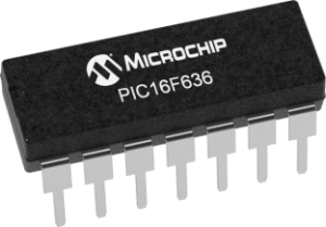
 Attack MCU PIC16F636 Binary
Attack MCU PIC16F636 Binary
Timer1 Operation in Asynchronous Counter Mode can greatly facilitate the process of Attack MCU PIC16F636 Binary.
If control bit T1SYNC (T1CON<2>) is set, the external clock input is not synchronized. The timer continues to increment asynchronous to the internal phase clocks. The timer will continue to run during SLEEP and can generate an interrupt on overflow, which will wake-up the processor. However, special precautions in software are needed to read/write the timer.
Timer1 Oscillator
A crystal oscillator circuit is built-in between pins OSC1 (input) and OSC2 (amplifier output). It is enabled by setting control bit T1OSCEN (T1CON<3>). The oscillator is a low power oscillator rated up to 32 kHz. It will continue to run during SLEEP. It is primarily intended for a 32 kHz crystal. Table 9-2 shows the capacitor selection for the Timer1 oscillator. The Timer1 oscillator is shared with the system LP oscillator. Thus, Timer1 can use this mode only when the system clock is derived from the internal oscillator.
Attack MCU PIC16F636 Binary
Asynchronous Counter Mode.
As with the system LP oscillator, the user must provide a software time delay to ensure proper oscillator start-up.
TRISA5 and TRISA4 bits are set when the Timer1 oscillator is enabled. RA5 and RA4 read as ‘0’ and TRISA5 and TRISA4 bits read as ‘1’
The Timer1 oscillator is shared with the system LP oscillator. Thus, Timer1 can use this mode only when the system clock is derived from the internal oscillator.
Reading TMR1H or TMR1L, while the timer is running from an external asynchronous clock, will ensure a valid read (taken care of in hardware). However, the user should keep in mind that reading the 16-bit timer oscillator is enabled. RA5 and RA4 read as ‘0’ and TRISA5 and TRISA4 bits read as ‘1’ in two 8-bit values itself, poses certain problems, since the timer may overflow between the reads.
For writes, it is recommended that the user simply stop the timer and write the desired values. A write contention may occur by writing to the timer registers, while the register is incrementing. This may produce an unpredictable value in the timer register before CLONE IC.
Reading the 16-bit value requires some care. Examples 12-2 and 12-3 in the PICmicro™ Mid-Range MCU Family Reference Manual (DS33023) show how to read and write Timer1 when it is running in Asynchronous mode.
Attack MCU PIC16F676 Code
Attack MCU PIC16F676 Code
This document contains device specific information for the PIC16F676. Additional information may be found in the PICmicroTM Mid-Range Reference Manual (DS33023) from Attack MCU PIC16F676 Code, which may be obtained from your local Microchip Sales Representative or downloaded from the Microchip web site.
The Reference Manual should be considered a complementary document to this Data Sheet and is highly recommended reading for a better understanding of the device architecture and operation of the peripheral modules.
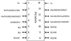
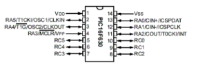
The PIC16F630 and PIC16F676 devices are covered by this Data Sheet. They are identical, except the PIC16F676 has a 10-bit A/D converter. They come in 14-pin PDIP, SOIC and TSSOP packages. Figure 1-1 shows a block diagram of the PIC16F630/676 devices. Table 1-1 shows the pinout description.
Attack MCU PIC16F676 Code
PROGRAM MEMORY ORGANIZATION
The PIC16F630/676 devices have a 13-bit program counter capable of addressing an 8K x 14 program memory space. Only the first 1K x 14 (0000h – 03FFh) for the PIC16F630/676 devices is physically implemented. Accessing a location above these boundaries will cause a wrap around within the first 1K x 14 space.
The RESET vector is at 0000h and the interrupt vector is at 0004h.
The data memory (see Figure 2-2) is partitioned into two banks, which contain the General Purpose registers and the Special Function registers. The Special Function registers are located in the first 32 locations of each bank. Register locations 20h-5Fh are General Purpose registers, implemented as static RAM and are mapped across both banks. All other RAM is unimplemented and returns ‘0’ when read. RP0 (STATUS<5>) is the bank select bit after CRACK MCU code.
SPECIAL FUNCTIONS REGISTERS
The Special Function registers are registers used by the CPU and peripheral functions for controlling the desired operation of the device (see Table 2-1). These registers are static RAM.
The special registers can be classified into two sets: core and peripheral. The Special Function registers associated with the “core” are described in this section. Those related to the operation of the peripheral features are described in the section of that peripheral feature.
Attack MCU PIC16F630 Firmware
Attack MCU PIC16F630 Firmware
Attack MCU PIC16F630 Firmware from its memory needs to take off the protection fuse bits of MCU and then set the status of MCU into unlocking, below its PIC16F630 features:
High Performance RISC CPU:
· Only 35 instructions to learn
– All single cycle instructions except branches
· Operating speed:
– DC – 20 MHz oscillator/clock input
– DC – 200 ns instruction cycle
· Interrupt capability
· 8-level deep hardware stack
· Direct, Indirect, and Relative Addressing modes
Attack MCU PIC16F630 Firmware
Special Microcontroller Features:
· Internal and external oscillator options
– Precision Internal 4 MHz oscillator factory calibrated to ±1%
– External Oscillator support for crystals and resonators
– 5 µs wake-up from SLEEP, 3.0V, typical
· Power saving SLEEP mode
· Wide operating voltage range – 2.0V to 5.5V
· Industrial and Extended temperature range
· Low power Power-on Reset (POR)
· Power-up Timer (PWRT) and Oscillator Start-up Timer (OST)
· Brown-out Detect (BOD)
· Watchdog Timer (WDT) with independent oscillator for reliable operation from CRACK MCU
· Multiplexed MCLR/Input-pin
· Interrupt-on-pin change
· Individual programmable weak pull-ups
· Programmable code protection
· High Endurance FLASH/EEPROM Cell
– 100,000 write FLASH endurance
– 1,000,000 write EEPROM endurance
– FLASH/Data EEPROM Retention: > 40 years
Low Power Features:
· Standby Current:
– 1 nA @ 2.0V, typical
· Operating Current:
– 8.5 µA @ 32 kHz, 2.0V, typical
– 100 µA @ 1 MHz, 2.0V, typical
· Watchdog Timer Current
– 300 nA @ 2.0V, typical
· Timer1 oscillator current:
– 4 µA @ 32 kHz, 2.0V, typical Peripheral Features
· 12 I/O pins with individual direction control
· High current sink/source for direct LED drive
· Analog comparator module with:
– Programmable on-chip comparator voltage reference (CVREF) module
– Programmable input multiplexing from device inputs
– Comparator output is externally accessible
· Analog-to-Digital Converter module (PIC16F676):
– 10-bit resolution
– Programmable 8-channel input
– Voltage reference input
· Timer0: 8-bit timer/counter with 8-bit programmable prescaler
· Enhanced Timer1:
– 16-bit timer/counter with prescaler
– External Gate Input mode
– Option to use OSC1 and OSC2 in LP mode as Timer1 oscillator, if INTOSC mode selected
· In-Circuit Serial ProgrammingTM (ICSPTM) via two pins
Attack MCU PIC12F675 Binary
Attack MCU PIC12F675 Binary
This document contains device specific information for the PIC12F675. Additional information may be found in the PIC® Mid-Range Reference Manual (DS33023) from Attack MCU PIC12F675 Binary, which may be obtained from your local Microchip Sales Representative or downloaded from the Microchip web site.
The Reference Manual should be considered a complementary document to this Data Sheet, and is highly recommended reading for a better understanding of the device architecture and operation of the peripheral modules.
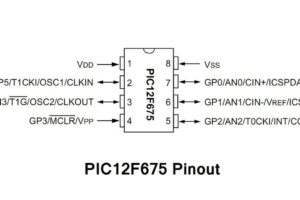
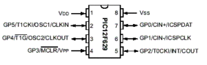
The PIC12F629 and PIC12F675 devices are covered by this Data Sheet. They are identical, except the PIC12F675 has a 10-bit A/D converter. They come in 8-pin PDIP, SOIC, MLF-S and DFN packages. Figure 1-1 shows a block diagram of the PIC12F675 devices. Below Table shows the pinout description.
Attack MCU PIC12F675 Binary
The PIC12F675 devices have a 13-bit program counter capable of addressing an 8K x 14 program memory space. Only the first 1K x 14 (0000h-03FFh) for the PIC12F629/675 devices is physically implemented. Accessing a location above these boundaries will cause a wrap-around within the first 1K x 14 space from UNLOCK MICROCONTROLLER.
The Reset vector is at 0000h and the interrupt vector is at 0004h.
The data memory (see Figure 2-2) is partitioned into two banks, which contain the General Purpose locations of each bank. Register locations 20h-5Fh are General Purpose Registers, implemented as static RAM and are mapped across both banks. All other RAM is unimplemented and returns ‘0’ when read. RP0 (STATUS<5>) is the bank select bit.
Registers and the Special Function Registers. The Special Function Registers are located in the first 32 locations of each bank. Register locations 20h-5Fh are General Purpose Registers, implemented as static RAM and are mapped across both banks. All other RAM is unimplemented and returns ‘0’ when read. RP0 (STATUS<5>) is the bank select bit.
Break IC PIC12F629 Program
Break IC PIC12F629 Program
Break IC PIC12F629 Program from its memory needs to decapsulate its silicon layer as well as metal layer, use probe to get access to the internal wafer die for databus probing:
High-Performance RISC CPU:
· Only 35 Instructions to Learn
– All single-cycle instructions except branches
· Operating Speed:
– DC – 20 MHz oscillator/clock input
– DC – 200 ns instruction cycle
· Interrupt Capability
· 8-Level Deep Hardware Stack
· Direct, Indirect, and Relative Addressing modes
Break IC PIC12F629 Program
Special Microcontroller Features:
· Internal and External Oscillator Options
– Precision Internal 4 MHz oscillator factory calibrated to ±1%
– External Oscillator support for crystals and resonators
– 5 ms wake-up from Sleep, 3.0V, typical
· Power-Saving Sleep mode
· Wide Operating Voltage Range – 2.0V to 5.5V
· Industrial and Extended Temperature Range
· Low-Power Power-on Reset (POR)
· Power-up Timer (PWRT) and Oscillator Start-up Timer (OST)
· Brown-out Detect (BOD)
· Watchdog Timer (WDT) with Independent Oscillator for Reliable Operation
· Multiplexed MCLR/Input Pin
· Interrupt-on-Pin Change
· Individual Programmable Weak Pull-ups
· Programmable Code Protection
· High Endurance Flash/EEPROM Cell
– 100,000 write Flash endurance
– 1,000,000 write EEPROM endurance
– Flash/Data EEPROM Retention: > 40 years
Low-Power Features:
· Standby Current:
– 1 nA @ 2.0V, typical
· Operating Current:
– 8.5 mA @ 32 kHz, 2.0V, typical
– 100 mA @ 1 MHz, 2.0V, typical
· Watchdog Timer Current
– 300 nA @ 2.0V, typical
· Timer1 Oscillator Current:
– 4 mA @ 32 kHz, 2.0V, typical
Peripheral Features:
· 6 I/O Pins with Individual Direction Control
· High Current Sink/Source for Direct LED Drive
· Analog Comparator module with:
– One analog comparator
– Programmable on-chip comparator voltage reference (CVREF) module
– Programmable input multiplexing from device inputs
– Comparator output is externally accessible
· Analog-to-Digital Converter module (PIC12F675):
– 10-bit resolution
– Programmable 4-channel input
– Voltage reference input
· Timer0: 8-Bit Timer/Counter with 8-Bit Programmable Prescaler
· Enhanced Timer1:
– 16-bit timer/counter with prescaler
– External Gate Input mode
– Option to use OSC1 and OSC2 in LP mode as Timer1 oscillator, if INTOSC mode selected
· In-Circuit Serial ProgrammingTM (ICSPTM) via two pins through CRACK MCU
Break IC PIC12F639 Heximal
Break IC PIC12F639 Heximal
Break IC PIC12F639 Heximal from its memory needs to know its memory organization
PROGRAM MEMORY ORGANIZATION
The PIC16F639 devices have a 13-bit program counter capable of addressing an 8K x 14 program memory space. Only the first 1K x 14 (0000h-03FFh, for the PIC12F635) and 2K x 14 (0000h-07FFh, for the PIC16F636/639) is physically implemented. Accessing a location above these boundaries will cause a wrap around within the first 2K x 14 space. The Reset vector is at 0000h and the interrupt vector is at 0004h.
DATA MEMORY ORGANIZATION
The data memory (see below Figure) is partitioned into two banks, which contain the General Purpose Registers (GPR) and the Special Function Registers (SFR).
The Special Function Registers are located in the first 32 locations of each bank. Register locations 20h-7Fh in Bank 0 and A0h-BFh in Bank 1 are GPRs, implemented as static RAM for the PIC16F639.For the PIC12F635, register locations 40h through 7Fh are GPRs implemented as static RAM. Register locations F0h-FFh in Bank 1 point to addresses 70h-7Fh in Bank 0. All other RAM is unimplemented and returns ‘0’ when read. RP0 (STATUS<5>) is the bank select bit.
GENERAL PURPOSE REGISTER
The register file is organized as 64 x 8 for the PIC12F635 and 128 x 8 for the PIC16F636/639. Each register is accessed, either directly or indirectly, through the File Select Register;
Break IC PIC12F639 Heximal
SPECIAL FUNCTION REGISTERS
The Special Function Registers (SFRs) are registers used by the CPU and peripheral functions for controlling the desired operation of the device. These registers are static RAM. The special registers can be classified into two sets: core and peripheral. The Special Function Registers associated with the “core” are described in this section. Those related to the operation of the peripheral features are described in the section of that peripheral feature from MCU CRACK.
Break IC PIC12F636 Code
Break IC PIC12F636 Code
it is also critical to know the peripheral features of PIC12F636 i the process of Break IC PIC12F636 Code:
Peripheral Features:
· 6/12 I/O pins with individual direction control:
– High-current source/sink for direct LED drive
– Interrupt-on-pin change
– Individually programmable weak pull-ups/pull-downs
– Ultra Low-Power Wake-up
· Analog comparator module with:
– Up to two analog comparators
– Programmable on-chip voltage reference (CVREF) module (% of VDD)
– Comparator inputs and outputs externally accessible
· Timer0: 8-bit timer/counter with 8-bit programmable prescaler
· Enhanced Timer1:
– 16-bit timer/counter with prescaler
– External Gate Input mode
– Option to use OSC1 and OSC2 in LP mode as Timer1 oscillator if INTOSC mode selected
· KEELOQ® compatible hardware Cryptographic module
· In-Circuit Serial ProgrammingTM (ICSPTM) via two pins
Break IC PIC12F636 Code
Low Frequency Analog Front-End Features (PIC16F639 only)
· Three input pins for 125 kHz LF input signals
· High input detection sensitivity (3 mVPP, typical)
· Demodulated data, Carrier clock or RSSI output selection
· Input carrier frequency: 125 kHz, typical
· Input modulation frequency: 4 kHz, maximum
· 8 internal configuration registers
· Bidirectional transponder communication (LF talk back)
· Programmable antenna tuning capacitance (up to 63 pF, 1 pF/step)
· Low standby current: 5 ìA (with 3 channels enabled), typical
· Low operating current: 15 ìA (with 3 channels enabled), typical
· Serial Peripheral Interface (SPI™) with internal MCU and external devices
· Supports Battery Back-up mode and batteryless operation with external circuits ly LOQ® compatible hardware Cryptographic module
· In-Circuit Serial ProgrammingTM (ICSPTM) IC breakion;
DEVICE OVERVIEW
This document contains device specific information for the PIC12F635/PIC16F636/639 devices. Additional information may be found in the “PICmicro® Mid-Range MCU Family Reference Manual” (DS33023), which may be obtained from your local Microchip Sales Representative or downloaded from the Microchip web site. The reference manual should be considered a complementary document to this data sheet and is highly recommended reading for a better understanding of the device architecture and operation of the peripheral modules for the purpose of CLONE IC.
Break IC PIC12F635 Program
Break IC PIC12F635 Program
Break IC PIC12F635 Program from eeprom and flash memory, and extract it out from it:
High-Performance RISC CPU:
· Only 35 instructions to learn:
– All single-cycle instructions except branches
· Operating speed:
– DC – 20 MHz oscillator/clock input
– DC – 200 ns instruction cycle
· Interrupt capability
· 8-level deep hardware stack
· Direct, Indirect and Relative Addressing modes
Special Microcontroller Features:
· Precision Internal Oscillator:
– Factory calibrated to ±1%
– Software selectable frequency range of 8 MHz to 31 kHz
– Software tunable
– Two-Speed Start-up mode
– Crystal fail detect for critical applications
· Clock mode switching for low power operation
· Power-saving Sleep mode
· Wide operating voltage range (2.0V-5.5V)
· Industrial and Extended Temperature range
· Power-on Reset (POR)
· Wake-up Reset (WUR)
· Independent weak pull-up/pull-down resistors
· Programmable Low-Voltage Detect (PLVD)
· Power-up Timer (PWRT) and Oscillator Start-up Timer (OST)
· Brown-out Detect (BOD) with software control option
· Enhanced Low-Current Watchdog Timer (WDT) with on-chip oscillator (software selectable nominal 268 seconds with full prescaler) with software enable
· Multiplexed Master Clear with pull-up/input pin
· Programmable code protection (program and data independent)
· High-Endurance Flash/EEPROM cell:
– 100,000 write Flash endurance
– 1,000,000 write EEPROM endurance
– Flash/Data EEPROM Retention: > 40 years
· Standby Current:
– 1 nA @ 2.0V, typical
· Operating Current:
– 8.5 ìA @ 32 kHz, 2.0V, typical
– 100 ìA @ 1 MHz, 2.0V, typical
– 1 ìA @ 2.0V, typical
Break IC PIC12F609 Heximal
Break IC PIC12F609 Heximal
Break IC PIC12F609 Heximal from eeprom and flash memory, and then transfer the heximal into other blank PIC12F609 which will provide the same functions:
Program Memory Organization
The PIC12F609 has a 13-bit program counter capable of addressing an 8K x 14 program memory space. Only the first 1K x 14 (0000h-03FFh) for the PIC12F609/615/12HV609/615 is physically implemented. Accessing a location above these boundaries will cause a wraparound within the first 1K x 14 space. The Reset vector is at 0000h and the interrupt vector is at 0004h.
Data Memory Organization
The data memory (see Figure 2-2) is partitioned into two banks, which contain the General Purpose Registers (GPR) and the Special Function Registers (SFR). The Special Function Registers are located in the first 32 locations of each bank.
Register locations 40h-7Fh in Bank 0 are General Purpose Registers, implemented as static RAM. Register locations F0h-FFh in Bank 1 point to addresses 70h-7Fh in Bank 0. All other RAM is unimplemented and returns ‘0’ when read. The RP0 bit of the STATUS register is the bank select bit.
Break IC PIC12F609 Heximal
The Special Function Registers are registers used by the CPU and peripheral functions for controlling the desired operation of the device. These registers are static RAM.
The special registers can be classified into two sets: core and peripheral. The Special Function Registers associated with the “core” are described in this section. Those related to the operation of the peripheral features are described in the section of that peripheral feature.
The STATUS register, shown in Register 2-1, contains:
· the arithmetic status of the ALU
· the Reset status
· the bank select bits for data memory (RAM)
The STATUS register can be the destination for any instruction, like any other register. If the STATUS register is the destination for an instruction that affects the Z, DC or C bits, then the write to these three bits is disabled. These bits are set or cleared according to the device logic. Furthermore, the TO and PD bits are not writable. Therefore, the result of an instruction with the STATUS register as destination may be different than intended for the purpose of CLONE IC.
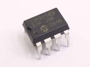
Break IC PIC12F615 Software
Break IC PIC12F615 Software
Break IC PIC12F615 Software from its memory, it is important to know the basic features of PIC12F615 and then disable its protection mechanism:
High-Performance RISC CPU:
· Only 35 instructions to learn:
– All single-cycle instructions except branches
· Operating speed:
– DC – 20 MHz oscillator/clock input
– DC – 200 ns instruction cycle
· Interrupt capability
· 8-level deep hardware stack
· Direct, Indirect and Relative Addressing modes
Special Microcontroller Features:
· Precision Internal Oscillator:
– Factory calibrated to ±1%, typical
– Software selectable frequency: 4 MHz or 8 MHz
· Power-Saving Sleep mode
· Voltage range:
– PIC12F609/615: 2.0V to 5.5V
– PIC12HV609/615: 2.0V to user defined maximum (see note)
· Industrial and Extended Temperature range
· Power-on Reset (POR)
· Power-up Timer (PWRT) and Oscillator Start-up Timer (OST)
· Brown-out Reset (BOR)
· Watchdog Timer (WDT) with independent oscillator for reliable operation
· Multiplexed Master Clear with pull-up/input pin
· Programmable code protection
· High Endurance Flash:
– 100,000 write Flash endurance
– Flash retention: > 40 years
Break IC PIC12F615 Software
Low-Power Features:
· Standby Current:
– 50 nA @ 2.0V, typical
· Operating Current:
– 11 ìA @ 32 kHz, 2.0V, typical
– 260 ìA @ 4 MHz, 2.0V, typical
· Watchdog Timer Current:
– 1 ìA @ 2.0V, typical
Peripheral Features:
· Shunt Voltage Regulator (PIC12HV609/615 only)
– 5 volt regulation
– 4 mA to 50 mA shunt range
· 5 I/O pins and 1 input only
· High current source/sink for direct LED drive
– Interrupt-on-pin change or pins
– Individually programmable weak pull-ups
· Analog Comparator module with:
– One analog comparator
– Programmable on-chip voltage reference (CVREF) module (% of VDD)
– Comparator inputs and output externally accessible
– Built-In Hysteresis (software selectable)
· Timer0: 8-bit timer/counter with 8-bit programmable prescaler
· Enhanced Timer1:
– 16-bit timer/counter with prescaler
– External Timer1 Gate (count enable)
– Option to use OSC1 and OSC2 in LP mode as Timer1 oscillator if INTOSC mode selected
– Option to use system clock as Timer1
· In-Circuit Serial ProgrammingTM (ICSPTM) via two pins
PIC12F615/HV615 ONLY:
· Enhanced Capture, Compare, PWM module:
– 16-bit Capture, max. resolution 12.5 ns
– Compare, max. resolution 200 ns
– 10-bit PWM with 1 or 2 output channels, 1 output channel programmable “dead time”, max. frequency 20 kHz, auto-shutdown
· A/D Converter:
– 10-bit resolution and 4 channels, samples internal voltage references
· Timer2: 8-bit timer/counter with 8-bit period register, prescaler and postscaler