 Recover Chip PIC12C509A Firmware
 May 24th, 2010 |
  Author:
 Recover Chip PIC12C509A Firmware from embedded memory, the program and data can be extracted from pic12c509a mcu and read out from secured microcontroller pic12c509a memory;
The same majority voting is done to the stop bit as done for the other bits in the frame. If the stop bit is registered to have a logic 0 value, the Frame Error (FEn) Flag will be set.
A new high to low transition indicating the start bit of a new frame can come right after the last of the bits used for majority voting. For Normal Speed mode, the first low level sample can be at point marked (A) in Figure 89 if Recover mcu stm32f107rct6 code firmware.
For Double Speed mode the first low level must be delayed to (B). (C) marks a stop bit of full length. The early start bit detection influences the operational range of the Receiver.
The operational range of the Receiver is dependent on the mismatch between the received bit rate and the internally generated baud rate after copy microcontroller pic16f684 memory.
If the Transmitter is sending frames at too fast or too slow bit rates, or the internally generated baud rate of the Receiver does not have a similar (see Table 99) base frequency, the Receiver will not be able to synchronize the frames to the start bit.
The following equations can be used to calculate the ratio of the incoming data rate and internal receiver baud rate. Sum of character size and parity size (D = 5 to 10 bit) Samples per bit. S = 16 for Normal Speed mode and S = 8 for Double Speed mode.
First sample number used for majority voting. SF = 8 for normal speed and SF = 4 for Double Speed mode. Middle sample number used for majority voting.
SM = 9 for normal speed and
SM = 5 for Double Speed mode.
Rslow is the ratio of the slowest incoming data rate that can be accepted in relation to the receiver baud rate. Rfast is the ratio of the fastest incoming data rate that can be accepted in relation to the receiver baud rate. Table 99 and Table 100 list the maximum receiver baud rate error that can be tolerated. Note that Normal Speed mode has higher toleration of baud rate variations after extract mcu pic16f54c hex.
Reverse Microcontroller PIC12C508A Firmware
Reverse Microcontroller PIC12C508A structure and extract code from embedded mcu pic12c508a flash memory, decrypt the Firmware of pic12c508a microprocessor;
The clock recovery logic synchronizes internal clock to the incoming serial frames. Figure 87 illustrates the sampling process of the start bit of an incoming frame.
The sample rate is 16 times the baud rate for Normal mode, and eight times the baud rate for Double Speed mode. The horizontal arrows illustrate the synchronization variation due to the sampling process. Note the larger time variation when using the Double Speed mode (U2Xn = 1) of operation. Samples denoted zero are samples done when the RxDn line is idle (i.e., no communication activity).
Please shown in the figure. The clock recovery logic then uses samples 8, 9, and 10 for Normal mode, and samples 4, 5, and 6 for Double Speed mode (indicated with sample numbers inside boxes on the figure), to decide if a valid start bit is received.
If two or more of these three samples have logical high levels (the majority wins), the start bit is rejected as a noise spike and the Receiver starts looking for the next high to low-transition.
If however, a valid start bit is detected, the clock recovery logic is synchronized and the data recovery can begin. The synchronization process is repeated for each start bit before Breaking IC.
When the receiver clock is synchronized to the start bit, the data recovery can begin. The data recovery unit uses a state machine that has 16 states for each bit in Normal mode and eight states for each bit in Double Speed mode.
Figure 88 shows the sampling of the data bits and the parity bit. Each of the samples is given a number that is equal to the state of the recovery unit.The decision of the logic level of the received bit is taken by doing a majority voting of the logic value to the three samples in the center of the received bit when Restore IC program.
The center samples are emphasized on the figure by having the sample number inside boxes. The majority voting process is done as follows: If two or all three samples have high levels, the received bit is registered to be a logic 1.
If two or all three samples have low levels, the received bit is registered to be a logic 0. This majority voting process acts as a low pass filter for the incoming signal on the RxDn pin.
The recovery process is then repeated until a complete frame is received. Including the first stop bit. Note that the Receiver only uses the first stop bit of a frame.
 Posted in Recover MCU |
  Tags: reverse microcontroller archive, reverse microcontroller bin, reverse microcontroller code, reverse microcontroller content, reverse microcontroller data, reverse microcontroller eeprom, reverse microcontroller file, reverse microcontroller firmware, reverse microcontroller hex, reverse microcontroller information, reverse microcontroller memory, reverse microcontroller program |
  Comments Closed
Break IC PIC16C57C Firmware
Break IC PIC16C57C Firmware is a process to unlock microcontroller pic16c57c encryptive system and then extract the embedded flash program from mcu pic16c57c memory;
The Parity Checker is active when the high USART Parity mode (UPMn1) bit is set. Type of Parity Check to be performed (odd or even) is selected by the UPMn0 bit.
When enabled, the Parity Checker calculates the parity of the data bits in incoming frames and compares the result with the parity bit from the serial frame.
The result of the check is stored in the receive buffer together with the received data and stop bits. The Parity Error (UPEn) Flag can then be read by software to check if the frame had a Parity Error before Break IC atmel atmega48pv memory.
The UPEn bit is set if the next character that can be read from the receive buffer had a Parity Error when received and the Parity Checking was enabled at that point (UPMn1 = 1). This bit is valid until the receive buffer (UDRn) is read.
In contrast to the Transmitter, disabling of the Receiver will be immediate. Data from ongoing receptions will therefore be lost. When disabled (i.e., the RXENn is set to zero) the Receiver will no longer override the normal function of the RxDn port pin before read mcu pic16f688 software.
The Receiver buffer FIFO will be flushed when the Receiver is disabled. Remaining data in the buffer will be lost. The receiver buffer FIFO will be flushed when the Receiver is disabled, i.e., the buffer will be emptied of its contents. Unread data will be lost. If the buffer has to be flushed during normal operation, due to for instance an error condition, read the UDRn I/O location until the RXCn Flag is cleared. The following firmware example shows how to flush the receive buffer.
The USART includes a clock recovery and a data recovery unit for handling asynchronous data reception. The clock recovery logic is used for synchronizing the internally generated baud rate clock to the incoming asynchronous serial frames at the RxDn pin after recover mcu st62t65c6 code.
The data recovery logic samples and low pass filters each incoming bit, thereby improving the noise immunity of the Receiver. The asynchronous reception operational range depends on the accuracy of the internal baud rate clock, the rate of the incoming frames, and the frame size in number of bits.
Reverse Engineering IC PIC18F248 Binary
Reverse Engineering IC PIC18F248 and locate the fuse bit position, crack mcu pic18f248 flash memory by focus ion beam and copy the embedded firmware from microcontroller pic18f248;
High-Performance RISC CPU:
· Linear program memory addressing up to 2 Mbytes
· Linear data memory addressing to 4 Kbytes
· Up to 10 MIPS operation
· DC – 40 MHz clock input
· 4 MHz-10 MHz oscillator/clock input with PLL active when copy microcontroller pic16f737 flash memory
· 16-bit wide instructions, 8-bit wide data path
· Priority levels for interrupts
· 8 x 8 Single-Cycle Hardware Multiplier
Peripheral Features:
· High current sink/source 25 mA/25 mA
· Three external interrupt pins
· Timer0 module: 8-bit/16-bit timer/counter with 8-bit programmable prescaler
· Timer1 module: 16-bit timer/counter
· Timer2 module: 8-bit timer/counter with 8-bit period register (time base for PWM)
· Timer3 module: 16-bit timer/counter
· Secondary oscillator clock option – Timer1/Timer3
· Capture/Compare/PWM (CCP) modules; CCP pins can be configured as:
– Capture input: 16-bit, max resolution 6.25 ns
– Compare: 16-bit, max resolution 100 ns (TCY) before break mcu pic18f442 software
– PWM output: PWM resolution is 1 to 10-bit Max. PWM freq. @:8-bit resolution = 156 kHz 10-bit resolution = 39 kHz
· Enhanced CCP module which has all the features of the standard CCP module, but also has the following features for advanced motor control:
– 1, 2 or 4 PWM outputs
– Selectable PWM polarity
– Programmable PWM dead time
· Master Synchronous Serial Port (MSSP) with two modes of operation:
– 3-wire SPI™ (Supports all 4 SPI modes) after Reverse engineering IC
– I2C™ Master and Slave mode
· Addressable USART module:
– Supports interrupt-on-address bit
Advanced Analog Features:
· 10-bit, up to 8-channel Analog-to-Digital Converter module (A/D) with:
– Conversion available during Sleep
– Up to 8 channels available
· Analog Comparator module:
– Programmable input and output multiplexing
· Comparator Voltage Reference module
· Programmable Low-Voltage Detection (LVD) module:
– Supports interrupt-on-Low-Voltage Detection
· Programmable Brown-out Reset (BOR)
CAN bus Module Features:
· Complies with ISO CAN Conformance Test
· Message bit rates up to 1 Mbps
· Conforms to CAN 2.0B Active Spec with:
– 29-bit Identifier Fields
– 8-byte message length
– 3 Transmit Message Buffers with prioritization
– 2 Receive Message Buffers
– 6 full, 29-bit Acceptance Filters
– Prioritization of Acceptance Filters
– Multiple Receive Buffers for High Priority Messages to prevent loss due to overflow
– Advanced Error Management Features
Special Microcontroller Features:
· Power-on Reset (POR), Power-up Timer (PWRT) and Oscillator Start-up Timer (OST)
· Watchdog Timer (WDT) with its own on-chip RC oscillator
· Programmable code protection
· Power-saving Sleep mode
· Selectable oscillator options, including:
– 4x Phase Lock Loop (PLL) of primary oscillator
– Secondary Oscillator (32 kHz) clock input
· In-Circuit Serial ProgrammingTM (ICSPTM) via two pins IC Flash Technology:
· Low-power, high-speed Enhanced Flash technology
· Fully static design Wide operating voltage range (2.0V to 5.5V) Industrial and Extended temperature ranges
Posted in Reverse Engineer Microcontroller |
Tags: reverse engineering IC protected binary, reverse engineering IC protected content, reverse engineering IC protected data, reverse engineering IC protected file, reverse engineering IC protected flash, reverse engineering IC protected heximal, reverse engineering IC protected software |
Comments Closed
Recovery IC PIC16F54C Program
Recovery IC PIC16F54C Program from its locked flash memory, crack mcu pic16f54c flash memory and extract locked heximal microcontroller pic16f54c;
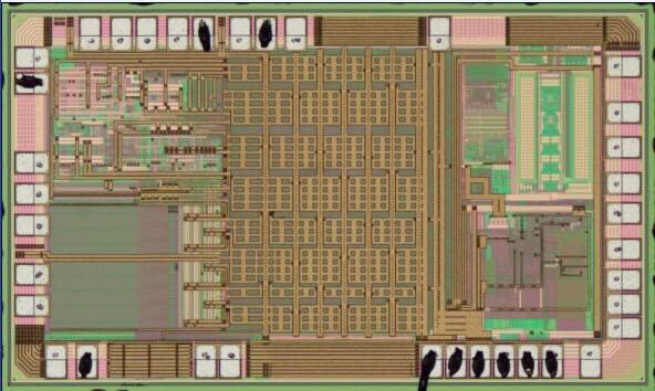
The USART Receiver has three Error Flags: Frame Error (FEn), Data OverRun (DORn) and Parity Error (UPEn). All can be accessed by reading UCSRnA. Common for the Error Flags is that they are located in the receive buffer together with the frame for which they indicate the error status.
Due to the buffering of the Error Flags, the UCSRnA must be read before the receive buffer (UDRn), since reading the UDRn I/O location changes the buffer read location. Another equality for the Error Flags is that they can not be altered by software doing a write to the flag location. However, all flags must be set to zero when the UCSRnA is written for upward compatibility of future USART implementations after Reverse mcu atmega461pv binary.
None of the Error Flags can generate interrupts. The Frame Error (FEn) Flag indicates the state of the first stop bit of the next readable frame stored in the receive buffer.
The FEn Flag is zero when the stop bit was correctly read (as one), and the FEn Flag will be one when the stop bit was incorrect (zero). This flag can be used for detecting out-of-sync conditions, detecting break conditions and protocol handling.
The FEn Flag is not affected by the setting of the USBSn bit in UCSRnC since the Receiver ignores all, except for the first, stop bits. For compatibility with future devices, always set this bit to zero when writing to UCSRnA before break atmega461p IC flash.
The Data OverRun (DORn) Flag indicates data loss due to a receiver buffer full condition. A Data OverRun occurs when the receive buffer is full (two characters), it is a new character waiting in the Receive Shift Register, and a new start bit is detected.
If the DORn Flag is set there was one or more serial frame lost between the frame last read from UDRn, and the next frame read from UDRn. For compatibility with future devices, always write this bit to zero when writing to UCSRnA. The DORn Flag is cleared when the frame received was successfully moved from the Shift Register to the receive buffer.
The Parity Error (UPEn) Flag indicates that the next frame in the receive buffer had a Parity Error when received. If Parity Check is not enabled the UPEn bit will always be read zero. For compatibility with future devices, always set this bit to zero when writing to UCSRnA. For more details see “Parity Bit Calculation” on page 210 and “Parity Checker”.
Posted in Recover Chip |
Tags: recovery ic archive, recovery ic bin, recovery ic code, recovery ic content, recovery ic data, recovery ic eeprom, recovery ic file, recovery ic firmware, recovery ic hex, recovery ic information, recovery ic memory, recovery ic program |
Comments Closed
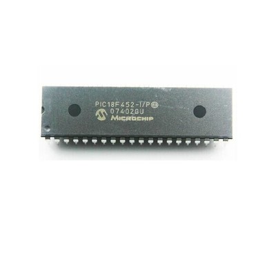
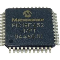
Recover MCU PIC18F452 Program
When embedded systems fail, are upgraded, or require inspection, access to the original firmware can be vital. Our service — summarized under the keyword Recover MCU PIC18F452 Program — helps legitimate owners and authorized technicians restore, readout, copy, clone, or duplicate the protected program held inside Microchip’s PIC18F452 MCU. We focus on recovering the firmware/binary/heximal image and producing usable outputs while respecting legal and ethical boundaries.
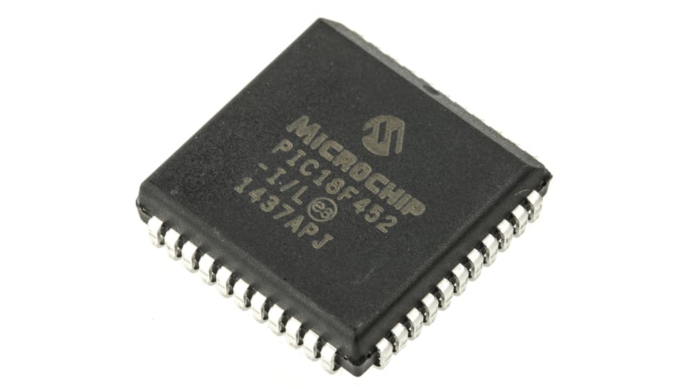
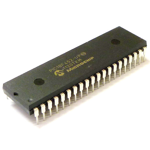
Recover MCU PIC18F452 Program starts from unlocking microcontroller pic18f452 secured memory and extract pic18f452 secured flash memory content;
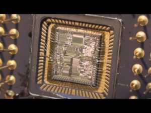
A “fast interrupt return” option is available for interrupts. A Fast Register Stack is provided for the STATUS, WREG and BSR registers and are only one in depth. The stack is not recoverable or writable and is loaded with the current value of the corresponding register when the processor vectors for an interrupt. The values in the registers are then loaded back into the working registers, if the FAST RETURN instruction is used to return from the interrupt.
A low or high priority interrupt source will push values into the stack registers. If both low and high priority interrupts are enabled, the stack registers cannot be used reliably for low priority interrupts. If a high priority interrupt occurs while servicing a low priority interrupt, the stack register values stored by the low priority interrupt will be overwritten if break pic12f635 MCU program.
Why clients need PIC18F452 program recovery
The PIC18F452 is a workhorse in many legacy and modern applications thanks to its flexible I/O, analog and timing peripherals, and on-chip nonvolatile memories. Devices built around this MCU often contain essential program files, calibration data, and archived memory that control hardware behavior. Typical reasons to request recovery include:
- Restore a device after accidental corruption or bad firmware updates.
- Duplicate/clone firmware for manufacturing spares or supporting legacy production.
- Migrate software to replacement hardware during end-of-life transitions.
- Audit or validate embedded code for safety, compliance, or forensic analysis.
What we do (high level, non-invasive)
Our service helps customers to legally open, unlock, decode, and extract the embedded flash/eeprom contents without publishing methods to bypass manufacturer protections. Key outcomes include:
- Verified extraction of the raw binary/heximal firmware image.
- Data integrity checks and documented checksums for recovery traceability.
- High-level decoding and annotated disassembly to aid engineers in understanding the recovered code.
- Delivery of recoverable files and a concise recovery report describing what was found and recommended next steps.
We do not provide procedural guidance to circumvent protections for unlawful purposes. All projects require proof of ownership or explicit authorization.
If high priority interrupts are not disabled during low priority interrupts, users must save the key registers in software during a low priority interrupt. If no interrupts are used, the fast register stack can be used to restore the STATUS, WREG and BSR registers at the end of a subroutine call. To use the fast register stack for a subroutine call, a FAST CALL instruction must be executed.
Example 4-1 shows a source code example that uses the fast register stack. The program counter (PC) specifies the address of the instruction to fetch for execution. The PC is 21-bits wide. The low byte is called the PCL register. This register is recoverable and writable. The high byte is called the PCH register. This register contains the PC<15:8> bits and is not directly recoverable or writable after break pic12f629 MCU program.
Updates to the PCH register may be performed through the PCLATH register. The upper byte is called PCU. This register contains the PC<20:16> bits and is not directly recoverable or writable. Updates to the PCU register may be performed through the PCLATU register.
The PC addresses bytes in the program memory. To prevent the PC from becoming misaligned with word instructions, the LSB of PCL is fixed to a value of ’0’. The PC increments by 2 to address sequential instructions in the program memory.
The CALL, RCALL, GOTO and program branch instructions write to the program counter directly. For these instructions, the contents of PCLATH and PCLATU are not transferred to the program counter.
Applications where PIC18F452 matters
The PIC18F452’s blend of digital control and analog support makes it common across multiple industries:
- Industrial controllers and instrumentation, where deterministic timing and ADCs matter.
- Consumer electronics and appliances, for feature logic and user interfaces.
- Automotive subsystems in legacy modules that use robust 8-bit control.
- Medical instruments and test equipment that rely on stable, well-tested firmware.
Because these systems often run long past their original support window, firmware recovery is frequently the only path to safe maintenance, calibration, or legal continuity.
Unique recovery considerations for PIC18F452
The PIC18F family commonly stores program code in on-chip flash with supplementary EEPROM for parameter data. Firmware may be protected, locked, or use custom bootloader schemes that complicate straightforward readout. Our approach combines careful chip identification, non-destructive readout methods, and conservative validation to minimize the risk of data loss. We prioritize preserving the device and its memory contents while delivering actionable artifacts to the customer.
The contents of PCLATH and PCLATU will be transferred to the program counter by an operation that writes PCL. Similarly, the upper two bytes of the program counter will be transferred to PCLATH and PCLATU by an operation that recovers PCL. This is useful for computed offsets to the PC.
The clock input (from OSC1) is internally divided by four to generate four non-overlapping quadrature clocks, namely Q1, Q2, Q3 and Q4. Internally, the program counter (PC) is incremented every Q1, the instruction is fetched from the program memory and latched into the instruction register in Q4.
The instruction is decoded and executed during the following Q1 through Q4. The clocks and instruction execution flow are shown in Figure 4-4. An “Instruction Cycle” consists of four Q cycles (Q1, Q2, Q3 and Q4). The instruction fetch and execute are pipelined such that fetch takes one instruction cycle, while decode and execute takes another instruction cycle;
However, due to the pipelining, each instruction effectively executes in one cycle. If an instruction causes the program counter to change (e.g., GOTO) then two cycles are required to complete the instruction (Example 4-2). The program memory is addressed in bytes. Instructions are stored as two bytes or four bytes in program memory.
The Least Significant Byte of an instruction word is always stored in a program memory location with an even address (LSB =’0’). Figure 4-5 shows an example of how instruction words are stored in the program memory. To maintain alignment with instruction boundaries, the PC increments in steps of 2 and the LSB will always recover ’0’ (see Section 4.4).
Clients receive the recovered heximal/binary file, a recovery certificate, and optional annotated disassembly to support debugging, porting, or re-engineering. Every engagement is governed by confidentiality agreements and an authorization check — our commitment is to lawful, ethical recovery for repair, backup, migration, or authorized analysis.
If you need to Recover MCU PIC18F452 Program — to restore, clone, or recover crucial program archives from a protected or secured device — our team provides secure, professional support that safeguards your data and operational continuity.
Break Chip ATmega162L Firmware
Break Chip ATmega162L and extract mcu atmega162 memory firmware, copy avr atmega162 flash memory content to new mcu atmega162;
If 9-bit characters are used (UCSZn=7) the ninth bit must be break from the RXB8n bit in UCSRnB before breaking the low bits from the UDRn. This rule applies to the FEn, DORn and UPEn Status Flags as well.
Break status from UCSRnA, then data from UDRn. Breaking the UDRn I/O location will change the state of the receive buffer FIFO and consequently the TXB8n, FEn, DORn and UPEn bits, which all are stored in the FIFO, will change if recover microprocessor atmega1281pa flash memory.
The following Firmware example shows a simple USART receive function that handles both nine bit characters and the status bits.
The receive function example breaks all the I/O Registers into the Register File before any computation is done. This gives an optimal receive buffer utilization since the buffer location break will be free to accept new data as early as possible after Break MCU ATmega2560pa hex.
The USART Receiver has one flag that indicates the Receiver state. The Receive Complete (RXCn) Flag indicates if there are unbreak data present in the receive buffer.
This flag is one when unbreak data exist in the receive buffer, and zero when the receive buffer is empty (i.e., does not contain any unbreak data). If the Receiver is disabled (RXENn = 0), the receive buffer will be flushed and consequently the RXCn bit will become zero.
When the Receive Complete Interrupt Enable (RXCIEn) in UCSRnB is set, the USART Receive Complete interrupt will be executed as long as the RXCn Flag is set (provided that global interrupts are enabled).
When interrupt-driven data reception is used, the receive complete routine must break the received data from UDRn in order to clear the RXCn Flag, otherwise a new interrupt will occur once the interrupt routine terminates.
Break MCU PIC18F442 Software
Break MCU PIC18F442 and extract embedded code from microcontroller pic18f442, the encrypted flash memory heximal of microprocessor pic18f442 will be unlocked;

The top of the stack is breakable and writable. Three register locations, TOSU, TOSH and TOSL hold the contents of the stack location pointed to by the STKPTR register. This allows users to implement a software stack if necessary.
After a CALL, RCALL or interrupt, the software can break the pushed value by breaking the TOSU, TOSH and TOSL registers. These values can be placed on a user defined software stack when Break pic16f88 Mcu data.
At return time, the software can replace the TOSU, TOSH and TOSL and do a return. The user must disable the global interrupt enable bits during this time to prevent inadvertent stack operations.
The STKPTR register contains the stack pointer value, the STKFUL (stack full) status bit, and the STKUNF (stack underflow) status bits. Register 4-1 shows the STKPTR register. The value of the stack pointer can be 0 through 31. The stack pointer increments when values are pushed onto the stack and decrements when values are popped off the stack. At RESET, the stack pointer value will be used to Breaking pic12ce518 Mcu.
The user may break and write the stack pointer value. This feature can be used by a Real Time Operating System for return stack maintenance. After the PC is pushed onto the stack 31 times (without popping any values off the stack), the STKFUL bit is set. The STKFUL bit can only be cleared in software or by a POR.
The action that takes place when the stack becomes full depends on the state of the STVREN (Stack Over-flow Reset Enable) configuration bit. Refer to Section 20.0 for a description of the device configuration bits.
If STVREN is set (default), the 31st push will push the (PC + 2) value onto the stack, set the STKFUL bit, and reset the device. The STKFUL bit will remain set and the stack pointer will be set to ‘0’.
If STVREN is cleared, the STKFUL bit will be set on the 31st push and the stack pointer will increment to 31. Any additional pushes will not overwrite the 31st push, and STKPTR will remain at 31.
Since the Top-of-Stack (TOS) is breakable and writable, the ability to push values onto the stack and pull values off the stack without disturbing normal program execution is a desirable option. To push the current PC value onto the stack, a PUSH instruction can be executed.
This will increment the stack pointer and load the current PC value onto the stack. TOSU, TOSH and TOSL can then be modified to place a return address on the stack.
The ability to pull the TOS value off of the stack and replace it with the value that was previously pushed onto the stack, without disturbing normal execution, is achieved by using the POP instruction. ThePOP instruction discards the current TOS by decrementing the stack pointer.
The previous value pushed onto the stack then becomes the TOS value. These resets are enabled by programming the STVREN configuration bit. When the STVREN bit is disabled, a full or underflow condition will set the appropriate STKFUL or STKUNF bit, but not cause a device RESET.
When the STVREN bit is enabled, a full or underflow will set the appropriate STKFUL or STKUNF bit and then cause a device RESET. The STKFUL or STKUNF bits are only cleared by the user software or a POR Reset.
Posted in Break IC |
Tags: break mcu protected archive, break mcu protected binary, break mcu protected code, break mcu protected content, break mcu protected data, break mcu protected eeprom, break mcu protected file, break mcu protected firmware, break mcu protected heximal, break mcu protected information, break mcu protected memory, break mcu protected program |
Comments Closed
Recover Microcontroller PIC18F252 Program
Recover Microcontroller PIC18F252 Program means the embedded heximal of mcu pic18f252 will be copied out from original flash memory after cracking protected mcu pic18f252.
Recover Microcontroller PIC18F252 Program means the embedded heximal of mcu pic18f252 will be copied out from original flash memory after cracking protected mcu pic18f252
CMOS Technology:
· Low power, high speed FLASH/EEPROM technology
· Fully static design
· Wide operating voltage range (2.0V to 5.5V)
· Industrial and Extended temperature ranges
· Low power consumption:
– < 1.6 mA typical @ 5V, 4 MHz
– 25 ìA typical @ 3V, 32 kHz
– < 0.2 ìA typical standby current
For timing-insensitive applications, the “RC” and “RCIO” device options offer additional cost savings.
The RC oscillator frequency is a function of the supply voltage, the resistor (REXT) and capacitor (CEXT) values and the operating temperature. In addition to this, the oscillator frequency will vary from unit to unit due to normal process parameter variation before copying pic16f627a microcontroller.
Furthermore, the difference in lead frame capacitance between package types will also affect the oscillation frequency, especially for low CEXT values. The user also needs to take into account variation due to tolerance of external R and C components used. Figure 2-3 shows how the R/C combination is connected.
In the RC Oscillator mode, the oscillator frequency divided by 4 is available on the OSC2 pin. This signal may be used for test purposes or to synchronize other logic.
The RCIO Oscillator mode functions like the RC mode, except that the OSC2 pin becomes an additional general purpose I/O pin. The I/O pin becomes bit 6 of PORTA (RA6).
The EC and ECIO Oscillator modes require an external clock source to be connected to the OSC1 pin. The feedback device between OSC1 and OSC2 is turned off in these modes to save current. There is no oscillator start-up time required after a Power-on Reset or after a recovery from SLEEP mode.
In the EC Oscillator mode, the oscillator frequency divided by 4 is available on the OSC2 pin. This signal may be used for test purposes or to synchronize other logic. Figure 2-4 shows the pin connections for the EC Oscillator mode.
Posted in Recover Chip |
Tags: microcontroller recoverying protected archive, microcontroller recoverying protected binary, microcontroller recoverying protected code, microcontroller recoverying protected content, microcontroller recoverying protected data, microcontroller recoverying protected eeprom, microcontroller recoverying protected file, microcontroller recoverying protected firmware, microcontroller recoverying protected heximal, microcontroller recoverying protected information, microcontroller recoverying protected memory, microcontroller recoverying protected program |
Comments Closed
Break IC PIC18F242 Software
Break IC PIC18F242 Software is a process to unlock encrypted mcu pic18f242 protection and open locked microcontroller pic18f242 flash memory silicon package;
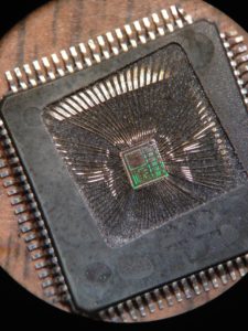
Break IC PIC18F242 Software is a process to unlock encrypted mcu pic18f242 protection and open locked microcontroller pic18f242 flash memory silicon package
High Performance RISC CPU:
· C compiler optimized architecture/instruction set
– Source code compatible with the PIC16 and PIC17 instruction sets
· Linear program memory addressing to 32 Kbytes
· Linear data memory addressing to 1.5 Kbytes
· Up to 10 MIPs operation:
– DC – 40 MHz osc./clock input
– 4 MHz – 10 MHz osc./clock input with PLL active
· 16-bit wide instructions, 8-bit wide data path
· Priority levels for interrupts
· 8 x 8 Single Cycle Hardware Multiplier
Peripheral Features:
· High current sink/source 25 mA/25 mA
· Three external interrupt pins
· Timer0 module: 8-bit/16-bit timer/counter with 8-bit programmable prescaler
· Timer1 module: 16-bit timer/counter
· Timer2 module: 8-bit timer/counter with 8-bit period register (time-base for PWM)
· Timer3 module: 16-bit timer/counter
· Secondary oscillator clock option – Timer1/Timer3
· Two Capture/Compare/PWM (CCP) modules. CCP pins that can be configured as:
– Capture input: capture is 16-bit, max. resolution 6.25 ns (TCY/16)
– Compare is 16-bit, max. resolution 100 ns (TCY)
– PWM output: PWM resolution is 1- to 10-bit, max. PWM freq. @: 8-bit resolution = 156 kHz 10-bit resolution = 39 kHz
· Master Synchronous Serial Port (MSSP) module,
Two modes of operation:
– 3-wire SPI™ (supports all 4 SPI modes)
– I2C™ Master and Slave mode
Peripheral Features (Continued):
· Addressable USART module:
– Supports RS-485 and RS-232
· Parallel Slave Port (PSP) module
Analog Features:
· Compatible 10-bit Analog-to-Digital Converter module (A/D):
– Fast sampling rate
– Conversion available during SLEEP
– Linearity ≤ 1 LSb
· Programmable Low Voltage Detection (PLVD)
– Supports interrupt on-Low Voltage Detection
· Programmable Brown-out Reset (BOR)
Posted in Reverse Engineer Microcontroller |
Tags: ic breaking embedded archive, ic breaking embedded binary, ic breaking embedded code, ic breaking embedded content, ic breaking embedded data, ic breaking embedded eeprom, ic breaking embedded file, ic breaking embedded firmware, ic breaking embedded heximal, ic breaking embedded information, ic breaking embedded memory, ic breaking embedded program |
Comments Closed