 Reverse Chip PIC12LC508 Heximal File
 June 9th, 2010 |
  Author:
 Reverse Chip PIC12LC508 Heximal File is a process to replicate cpu pic12lf508 program from memory, and then extract the code from pic12lf508 locked flash memory.
A serial frame for the MSPIM is defined to be one character of 8 data bits. The USART in MSPIM mode has two valid frame formats:
8-bit data with MSB first
8-bit data with LSB first
A frame starts with the least or most significant data bit. Then the next data bits, up to a total of eight, are succeeding, ending with the most or least significant bit accordingly when attack mcu aduc831bsz firmware Heximal file.
When a complete frame is transmitted, a new frame can directly follow it, or the communication line can be set to an idle (high) state.
The UDORDn bit in UCSRnC sets the frame format used by the USART in MSPIM mode. The Receiver and Transmitter use the same setting. Note that changing the setting of any of these bits will corrupt all ongoing communication for both the Receiver and Transmitter before attack mcu tms320f28027pta CHIP.
16-bit data transfer can be achieved by writing two data bytes to UDRn. A UART transmit complete interrupt will then signal that the 16-bit value has been shifted out.
The USART in MSPIM mode has to be initialized before any communication can take place. The initialization process normally consists of setting the baud rate, setting master mode of operation (by setting DDR_XCKn to one), setting frame format and enabling the Transmitter and the Receiver.
Only the transmitter can operate independently. For interrupt driven USART operation, the Global Interrupt Flag should be cleared (and thus interrupts globally disabled) when doing the initialization.
Note:
To ensure immediate initialization of the XCKn output the baud-rate register (UBRRn) must be zero at the time the transmitter is enabled.
Contrary to the normal mode USART operation the UBRRn must then be written to the desired value after the transmitter is enabled, but before the first transmission is started after copy pic16lf877 program.
Setting UBRRn to zero before enabling the transmitter is not necessary if the initialization is done immediately after a reset since UBRRn is reset to zero.
Before doing a re-initialization with changed baud rate, data mode, or frame format, be sure that there is no ongoing transmissions during the period the registers are changed if copy mcu pic18f2480 program.
The TXCn Flag can be used to check that the Transmitter has completed all transfers, and the RXCn Flag can be used to check that there are no unread data in the receive buffer.
Note that the TXCn Flag must be cleared before each transmission (before UDRn is written) if it is used for this purpose. The following simple USART initialization heximal file examples show one assembly and one C function that are equal in functionality.
The examples assume polling (no interrupts enabled). The baud rate is given as a function parameter. For the assembly heximal file, the baud rate parameter is assumed to be stored in the r17:r16 registers.
 Posted in Recover Chip |
  Tags: reverse mcu bin, reverse mcu code, reverse mcu data, reverse mcu eeprom, reverse mcu file, reverse mcu firmware, reverse mcu hex, reverse mcu lock bit, reverse mcu memory, reverse mcu program, reverse mcu security bits, reverse mcu software |
  Comments Closed
Break Chip ATmega8A Binary
Break Chip ATmega8A and extract microcontroller atmega8a Binary from its flash memory, copy mcu atmega8a heximal out and then download to the new mcu to serve as the same functionality;
First Analog Comparator conversion may be delayed
If the device is powered by a slow rising VCC, the first Analog Comparator conversion will take longer than expected on some devices. Problem Fix/Workaround, When the device has been powered or reset, disable then enable theAnalog Comparator before the first conversion.
Interrupts may be lost when writing the timer registers in the asynchronous timer If one of the timer registers which is synchronized to the asynchronous timer2 clock is written in the cycle before a overflow interrupt occurs, the interrupt may be lost if attack atmega Chip flash memory.
Problem Fix/Workaround Always check that the Timer2 Timer/Counter register, TCNT2, does not have the value 0xFF before writing the Timer2 Control Register, TCCR2, or Output Compare Register, OCR2
Signature may be Erased in Serial Programming Mode If the signature bytes are read before a chiperase command is completed, the signature may be erased causing the device ID and calibration bytes to disappear. This is critical, especially, if the part is running on internal RC oscillator.
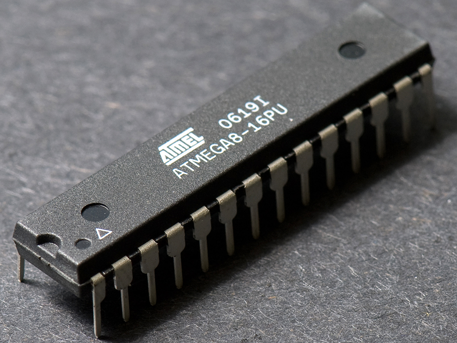
attack ATmega8A microprocessor protective system and restore heximal file from ATmega8A mcu flash memory
Problem Fix/Workaround: Ensure that the chiperase command has exceeded before applying the next command.
CKOPT Does not Enable Internal Capacitors on XTALn/TOSCn Pins when 32 KHz Oscillator is Used to Clock the Asynchronous Timer/Counter2 When the internal RC Oscillator is used as the main clock source, it is possible to run the Timer/Counter2 asynchronously by connecting a 32 KHz Oscillator between XTAL1/TOSC1 and XTAL2/TOSC2.
But when the internal RC Oscillator is selected as the main clock source, the CKOPT Fuse does not control the internal capacitors on XTAL1/TOSC1 and XTAL2/TOSC2. As long as there are no capacitors connected to XTAL1/TOSC1 and XTAL2/TOSC2, safe operation of the Oscillator is not guaranteed if attack dsp mcu Chip flash memory.
Problem fix/Workaround
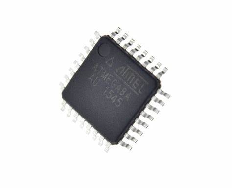
secured microcontroller atmega8a security fuse bit cracking to readout embedded program from atmega8a mcu flash memory
Use external capacitors in the range of 20 – 36 pF on XTAL1/TOSC1 and XTAL2/TOSC2. This will be fixed in ATmega8 Rev. G where the CKOPT Fuse will control internal capacitors also when internal RC Oscillator is selected as main clock source. For ATmega8 Rev. G, CKOPT = 0 (programmed) will enable the internal capacitors on XTAL1 and XTAL2. Customers who want compatibility between Rev.
G and older revisions, must ensure that CKOPT is unprogrammed (CKOPT = 1).
1
Updated Some Preliminary Test Limits and Characterization Data
The following tables have been updated:
Table 15, “Reset Characteristics,” on page 38, Table 16, “Internal Voltage Reference Characteristics,” on page 42, DC Characteristics on page 242, Table , “ADC Characteristics,” on page 248.
Changes in External Clock Frequency
Added the description at the end of “External Clock” on page 32.
Added period changing data in Table 99, “External Clock Drive,” on page 244.
Updated TWI Chapter
More details regarding use of the TWI bit rate prescaler and a Table 65, “TWI Bit
Rate Prescaler,” on page 173.
Updated Typical Start-up Times.
The following tables has been updated:
Table 5, “Start-up Times for the Crystal Oscillator Clock Selection,” on page 28,
Table 6, “Start-up Times for the Low-frequency Crystal Oscillator Clock Selection,”
on page 28, Table 8, “Start-up Times for the External RC Oscillator Clock Selection,” on page 29, and Table 12, “Start-up Times for the External Clock Selection,” on page 32 if Break Chip.
Posted in Break IC |
Tags: crack mcu atmega8a flash, microprocessore di attacco atmega8a, rompere la memoria del microcontrollore atmega8a |
Comments Closed
Decap IC PIC16C55 Eeprom
Decap IC PIC16C55 Eeprom and extract mcu pic16c55 heximal from flash memory, and clone firmware to new microcontroller pic16c55 to provide the same functions;
Setting both UMSELn1:0 bits to one enables the USART in MSPIM logic. In this mode of operation the SPI master control logic takes direct control over the USART resources.
These resources include the transmitter and receiver shift register and buffers, and the baud rate generator. The parity generator and checker, the data and clock recovery logic, and the RX and TX control logic is disabled if recover mcu pic16f873 hex.
The USART RX and TX control logic is replaced by a common SPI transfer control logic. However, the pin control logic and interrupt generation logic is identical in both modes of operation.
The I/O register locations are the same in both modes. However, some of the functionality of the control registers changes when using MSPIM before recover mcu dspic30f6013 firmware.
The Clock Generation logic generates the base clock for the Transmitter and Receiver. For USART MSPIM mode of operation only internal clock generation (i.e. master operation) is supported.
The Data Direction Register for the XCKn pin (DDR_XCKn) must therefore be set to one (i.e. as output) for the USART in MSPIM to operate correctly when break mcu at89c5131a IC.
Preferably the DDR_XCKn should be set up before the USART in MSPIM is enabled (i.e. TXENn and RXENn bit set to one). The internal clock generation used in MSPIM mode is identical to the USART synchronous master mode.
The baud rate or UBRRn setting can therefore be calculated using the same equations, see Table 110: Table 110. Equations for Calculating Baud Rate Register Setting There are four combinations of XCKn (SCK) phase and polarity with respect to serial data, which are determined by control bits UCPHAn and UCPOLn.
The data transfer timing diagrams are shown in Figure 90. Data bits are shifted out and latched in on opposite edges of the XCKn signal, ensuring sufficient time for data signals to stabilize.
The UCPOLn and UCPHAn functionality is summarized in Table 111. Note that changing the setting of any of these bits will corrupt all ongoing communication for both the Receiver and Transmitter.
Posted in Recover MCU |
Tags: decap ic bin, decap ic code, decap ic data, decap ic eeprom, decap ic file, decap ic firmware, decap ic fuse bits, decap ic hex, decap ic memory, decap ic security bits, decap ic software |
Comments Closed
Clone Microcontroller PIC16C54 Heximal
Clone Microcontroller PIC16C54 Heximal is a process to duplicate microcontroller pic16c54 memory program from flash and eeprom, firmware will be extracted from mcu pic16c54 after break it;
Bit 15:12 – Reserved Bits
These bits are reserved for future use. For compatibility with future devices, these bit must be written to zero when UBRRH is written.
Bit 11:0 – UBRR11:0: USART Baud Rate Register
This is a 12-bit register which contains the USART baud rate. The UBRRH contains the four most significant bits, and the UBRRL contains the eight least significant bits of the USART baud rate if attack pic18f66k90 microcontroller hex.
Ongoing transmissions by the Transmitter and Receiver will be corrupted if the baud rate is changed. Writing UBRRL will trigger an immediate update of the baud rate prescaler.
For standard crystal and resonator frequencies, the most commonly used baud rates for asynchronous operation can be generated by using the UBRR settings in Table 106 to Table 109.
UBRR values which yield an actual baud rate differing less than 0.5% from the target baud rate, are bold in the table. Higher error ratings are acceptable, but the Receiver will have less noise resistance when the error ratings are high, especially for large serial frames (see “Asynchronous Operational Range” on page 220) when Copy pic18f458 MICROCONTROLLER hex.
The error values are calculated using the following equation:
BaudRateClosest Match
⎝ BaudRate ⎠
The Universal Synchronous and Asynchronous serial Receiver and Transmitter (USART) can be set to a master SPI compliant mode of operation. The Master SPI Mode (MSPIM) has the following features:
Full Duplex, Three-wire Synchronous Data Transfer
Master Operation
Supports all four SPI Modes of Operation (Mode 0, 1, 2, and 3)
LSB First or MSB First Data Transfer (Configurable Data Order)
Queued Operation (Double Buffered)
High Resolution Baud Rate Generator
High Speed Operation (fXCKmax = fCK/2)
Flexible Interrupt Generation
Posted in Break IC |
Tags: clone microcontroller bin, clone microcontroller code, clone microcontroller data, clone microcontroller eeprom, clone microcontroller file, clone microcontroller firmware, clone microcontroller fuse bit, clone microcontroller hex, clone microcontroller lock bit, clone microcontroller memory, clone microcontroller program, clone microcontroller software |
Comments Closed
Decap IC PIC16C54A Heximal file
Decap IC PIC16C54A and clone microcomputer pic16c54a memory content, and read mcu pic16c54a Heximal file out from its flash and eeprom memory;
Bit 4 – RXENn: Receiver Enable n
Writing this bit to one enables the USART Receiver. The Receiver will override normal port operation for the RxDn pin when enabled. Disabling the Receiver will flush the receive buffer invalidating the FEn, DORn, and UPEn Flags when copy microcontroller at89c51re2 bin file.
Bit 3 – TXENn: Transmitter Enable n
Writing this bit to one enables the USART Transmitter. The Transmitter will override normal port operation for the TxDn pin when enabled.
The disabling of the Transmitter (writing TXENn to zero) will not become effective until ongoing and pending transmissions are completed, i.e., when the Transmit Shift Register and Transmit Buffer Register do not contain data to be transmitted. When disabled, the Transmitter will no longer override the TxDn port.
Bit 2 – UCSZn2: Character Size n
The UCSZn2 bits combined with the UCSZn1:0 bit in UCSRnC sets the number of data bits (Character SiZe) in a frame the Receiver and Transmitter use after recover IC c8051f340 hex file.
Bit 1 – RXB8n: Receive Data Bit 8 n
RXB8n is the ninth data bit of the received character when operating with serial frames with nine data bits. Must be decap before decaping the low bits from UDRn when break IC STM32F101C4T6 hex file.
Bit 0 – TXB8n: Transmit Data Bit 8 n
TXB8n is the ninth data bit in the character to be transmitted when operating with serial frames with nine data bits. Must be written before writing the low bits to UDRn.
Bits 7:6 – UMSELn1:0 USART Mode Select
These bits select the mode of operation of the USARTn as shown in Table 101..
Bits 5:4 – UPMn1:0: Parity Mode
These bits enable and set type of parity generation and check. If enabled, the Transmitter will automatically generate and send the parity of the transmitted data bits within each frame.
The Receiver will generate a parity value for the incoming data and compare it to the UPMn setting. If a mismatch is detected, the UPEn Flag in UCSRnA will be set.
Bit 3 – USBSn: Stop Bit Select
This bit selects the number of stop bits to be inserted by the Transmitter. The Receiver ignores this setting.
Posted in Recover MCU |
Tags: decap ic bin, decap ic code, decap ic content, decap ic data, decap ic eeprom, decap ic file, decap ic firmware, decap ic flash, decap ic hex, decap ic lock bit, decap ic memory, decap ic program, decap ic software |
Comments Closed
Open IC PIC16C52 Program
Open IC PIC16C52 and unlock mcu pic16c52 flash memory, extract embedded Program from microcontroller pic16c52 flash and eeprom memory in the format of heximal or binary;
This bit is set if the next character in the receive buffer had a Frame Error when received. I.e., when the first stop bit of the next character in the receive buffer is zero.
This bit is valid until the receive buffer (UDRn) is read. The FEn bit is zero when the stop bit of received data is one. Always set this bit to zero when writing to UCSRnA. This bit is set if a Data OverRun condition is detected. A Data OverRun occurs when the receive buffer is full (two characters), it is a new character waiting in the Receive Shift Register, and a new start bit is detected.
This bit is valid until the receive buffer (UDRn) is read. Always set this bit to zero when writing to UCSRnA. This bit is set if the next character in the receive buffer had a Parity Error when received and the Parity Checking was enabled at that point (UPMn1 = 1).
This bit is valid until the receive buffer (UDRn) is read. Always set this bit to zero when writing to UCSRnA. This bit only has effect for the asynchronous operation. Write this bit to zero when using synchronous operation when copy pic16f886 IC firmware program.
Writing this bit to one will reduce the divisor of the baud rate divider from 16 to 8 effectively doubling the transfer rate for asynchronous communication. This bit enables the Multi-processor Communication mode.
When the MPCMn bit is written to one, all the incoming frames received by the USART Receiver that do not contain address information will be ignored. The Transmitter is unaffected by the MPCMn setting. For more detailed information see “Multi-processor Communication Mode” on page 221. Writing this bit to one enables interrupt on the RXCn Flag. A USART Receive Complete interrupt will be generated only if the RXCIEn bit is written to one, the Global Interrupt Flag in SREG is written to one and the RXCn bit in UCSRnA is set after attack mcu atmega162 flash memory.
Writing this bit to one enables interrupt on the TXCn Flag. A USART Transmit Complete interrupt will be generated only if the TXCIEn bit is written to one, the Global Interrupt Flag in SREG is written to one and the TXCn bit in UCSRnA is set.
Writing this bit to one enables interrupt on the UDREn Flag. A Data Register Empty interrupt will be generated only if the UDRIEn bit is written to one, the Global Interrupt Flag in SREG is written to one and the UDREn bit in UCSRnA is set after attack chip pic16f72 memory.
Posted in Recover Chip |
Tags: open ic bin, open ic code, open ic content, open ic data, open ic eeprom, open ic file, open ic firmware, open ic hex, open ic lock bits, open ic memory, open ic program, open ic software |
Comments Closed
Recovery Chip PIC16C505 Eeprom
Recovery Chip PIC16C505 Eeprom content needs to crack pic16c505 mcu protection and extract embedded firmware from microcontroller pic16c505;
The USART Transmit Data Buffer Register and USART Receive Data Buffer Registers share the same I/O address referred to as USART Data Register or UDRn. The Transmit Data Buffer Register (TXB) will be the destination for data written to the UDRn Register location.
Reading the UDRn Register location will return the contents of the Receive Data Buffer Register (RXB). For 5-, 6-, or 7-bit characters the upper unused bits will be ignored by the Transmitter and set to zero by the Receiver if copy microcontroller p87c51x2bbd.
The transmit buffer can only be written when the UDREn Flag in the UCSRnA Register is set. Data written to UDRn when the UDREn Flag is not set, will be ignored by the USART Transmitter.
When data is written to the transmit buffer, and the Transmitter is enabled, the Transmitter will load the data into the Transmit Shift Register when the Shift Register is empty. Then the data will be serially transmitted on the TxDn pin. The receive buffer consists of a two level FIFO. The FIFO will change its state whenever the receive buffer is accessed. Due to this behavior of the receive buffer, do not use Read-Modify-Write instructions (SBI and CBI) on this location if Recovery mcu pic18f2520 bin.
Be careful when using bit test instructions (SBIC and SBIS), since these also will change the state of the FIFO. This flag bit is set when there are unread data in the receive buffer and cleared when the receive buffer is empty (i.e., does not contain any unread data).
If the Receiver is disabled, the receive buffer will be flushed and consequently the RXCn bit will become zero. The RXCn Flag can be used to generate a Receive Complete interrupt (see description of the RXCIEn bit) before Recovery Chip mc68hc11a0fn3 binary.
This flag bit is set when the entire frame in the Transmit Shift Register has been shifted out and there are no new data currently present in the transmit buffer (UDRn). The TXCn Flag bit is automatically cleared when a transmit complete interrupt is executed, or it can be cleared by writing a one to its bit location. The TXCn Flag can generate a Transmit Complete interrupt (see description of the TXCIEn bit).
The UDREn Flag indicates if the transmit buffer (UDRn) is ready to receive new data. If UDREn is one, the buffer is empty, and therefore ready to be written. The UDREn Flag can generate a Data Register Empty interrupt (see description of the UDRIEn bit). UDREn is set after a reset to indicate that the Transmitter is ready.
Posted in Recover Chip |
Tags: recover chip protected archive, recover chip protected bin, recover chip protected code, recover chip protected content, recover chip protected data, recover chip protected eeprom, recover chip protected file, recover chip protected firmware, recover chip protected hex, recover chip protected information, recover chip protected memory, recover chip protected program |
Comments Closed
Break MCU AT89C5131A Binary
The ATMEL AT89C5131A is a powerful microcontroller (MCU) widely adopted across industries due to its versatility and integrated USB interface. As part of the AT89C51 family, it combines a high-performance 8-bit microprocessor core with on-chip flash, EEPROM, and multiple communication peripherals. These features make it highly reliable for use in industrial controllers, consumer devices, medical equipment, and security products. However, when the firmware becomes inaccessible, or the binary program is locked by security settings, companies may require specialized services to break MCU AT89C5131A binary for legitimate recovery, duplication, or system maintenance.
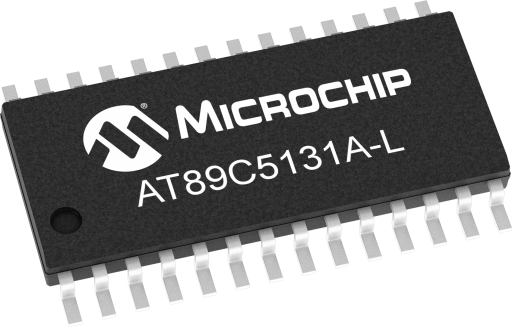
The AT89C5131A is commonly applied in:
- Industrial Control Systems – handling automation tasks, sensor data management, and device control.
- Medical Electronics – used in diagnostic instruments where stable firmware and reliable memory archives are essential.
- Consumer Electronics – powering USB-based devices, smart accessories, and portable tools.
- Security Systems – embedded in access control solutions and cryptographic devices, where secured and encrypted programs protect sensitive data.
These real-world applications highlight the importance of the source code and binary files stored in the chip’s flash and EEPROM memory. When a system malfunctions or legacy firmware is required, the ability to retrieve, restore, or replicate these files becomes critical.
Break MCU AT89C5131A needs to unlock microcontroller at89c5131a fuse bit among flash memory and processor, then extract ic chip Binary from it;
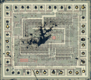
AT89C5130A/31A-M is a high-performance Flash version of the 80C51 single-chip 8-bit micro-controllers with full speed USB functions. AT89C5130A/31A-M features a full-speed USB module compatible with the USB specifications Version 1.1 and 2.0.
The AT89C5131A includes strong protection mechanisms to secure its embedded program from unauthorized readout or copying. Once code protection is enabled, the device’s flash memory becomes locked, preventing standard access. Key difficulties include:
- Secured Flash and EEPROM – Direct extraction of firmware is blocked by built-in protection bits.
- Encrypted Program Storage – Data is often stored in protected formats, requiring advanced decode and decrypt expertise.
- Tamper Resistance – Some chips may erase their memory if invasive attack attempts are detected.
- Reverse Engineering Complexity – Even if partial dump files are collected, reconstructing complete heximal archives demands expert knowledge.
These challenges mean that attempts to unlock, hack, or decapsulate the device require highly specialized approaches.
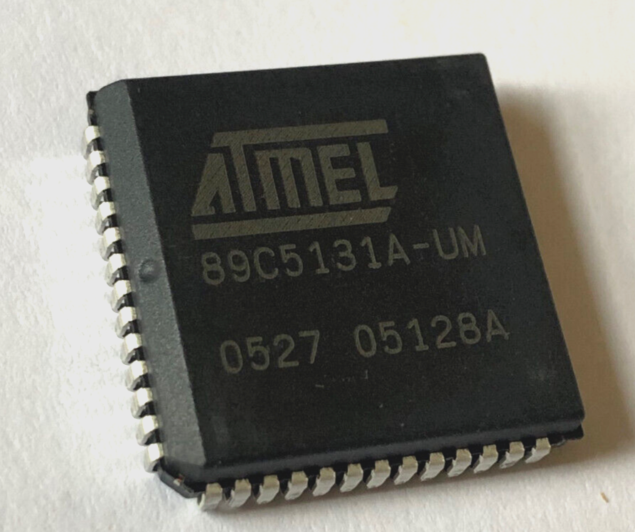
This module integrates the USB transceivers with a 3.3V voltage regulator and the Serial Interface Engine (SIE) with Digital Phase Locked Loop and 48 MHz clock recovery after recover stm32f107rct6 MCU.
USB Event detection logic (Reset and Suspend/Resume) and FIFO buffers supporting the mandatory control Endpoint (EP0) and up to 6 versatile Endpoints (EP1/EP2/EP3/EP4/EP5/EP6) with minimum software overhead are also part of the USB module.
AT89C5130A/31A-M retains the features of the Atmel 80C52 with extended Flash capacity (16/32-Kbytes), 256 bytes of internal RAM, a 4-level interrupt system, two 16-bit timer/counters (T0/T1), a full duplex enhanced UART (EUART) and an on-chip oscillator.
In addition, AT89C5130A/31A-M has an on-chip expanded RAM of 1024 bytes (ERAM), a dual data pointer, a 16-bit up/down Timer (T2), a Programmable Counter Array (PCA), up to 4 programmable LED current sources, a programmable hardware watchdog and a power-on reset for copy at89s8252 MCU flash.
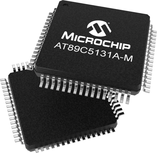
We provide the complete solution for organizations needing to break MCU AT89C5131A binary in a secure, reliable, and legally compliant manner. Our team combines advanced reverse engineering expertise with precision tools to extract, readout, and recover embedded firmware while maintaining the integrity of the original chip.
Our services include:
- Firmware Recovery and Restoration – enabling customers to restore essential files from locked devices.
- Cloning and Replication – safely duplicate or copy the program onto new hardware for production continuity.
- Legacy System Support – helping industries extend the life of older systems by retrieving embedded firmware.
We do not simply attempt brute-force attacks; instead, we employ professional methods that minimize risk, preserve data, and ensure consistent results.
AT89C5130A/31A-M has two software-selectable modes of reduced activity for further reduction in power consumption. In the idle mode the CPU is frozen while the timers, the serial ports and the interrupt system are still operating. In the power-down mode the RAM is saved, the peripheral clock is frozen, but the device has full wake-up capability through USB events or external interrupts.
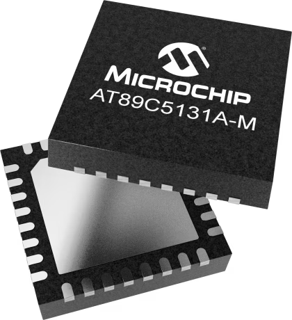
The need to break MCU AT89C5131A binary arises when businesses face locked or inaccessible systems that hinder ongoing operations. With applications across critical industries, the ability to recover, replicate, and restore firmware is invaluable. Our proven services offer a perfect solution, ensuring that your secured MCU can be successfully unlocked and its binary data fully retrieved for future use.
Posted in Break IC |
Tags: break mcu locked archive, break mcu locked code, break mcu locked dump, break mcu locked eeprom, break mcu locked firmware, break mcu locked information, break mcu locked memory, break mcu locked program, знаходзіць зноў locked mcu binary, знаходзіць зноў locked mcu data, знаходзіць зноў locked mcu eeprom, знаходзіць зноў locked mcu file, знаходзіць зноў locked mcu firmware, знаходзіць зноў locked mcu heximal, знаходзіць зноў locked mcu memory, знаходзіць зноў locked mcu program |
Comments Closed
Break Chip PIC12C509 Code
Break Chip PIC12C509 and extract mcu pic12c509 Code from embedded flash memory, microcontroller pic12c509 memory program will be readout after crack fuse bit by focus ion beam technique;
For an CHIP to act as a master CHIP, it can use a 9-bit character frame format (UCSZn = 7). The ninth bit (TXB8n) must be set when an address frame (TXB8n = 1) or cleared when a data frame (TXB = 0) is being transmitted.
The slave CHIPs must in this case be set to use a 9-bit character frame format. The following procedure should be used to exchange data in Multi-processor Communication mode:
All Slave CHIPs are in Multi-processor Communication mode (MPCMn in UCS-RnA is set).
The Master CHIP sends an address frame, and all slaves receive and break this frame. In the Slave CHIPs, the RXCn Flag in UCSRnA will be set as normal before reverse atmega162 CHIP heximal code.
Each Slave CHIP breaks the UDRn Register and determines if it has been selected. If so, it clears the MPCMn bit in UCSRnA, otherwise it waits for the next address byte and keeps the MPCMn setting.
The addressed CHIP will receive all data frames until a new address frame is received. The other Slave CHIPs, which still have the MPCMn bit set, will ignore the data frames.
When the last data frame is received by the addressed CHIP, the addressed CHIP sets the MPCMn bit and waits for a new address frame from master. The process then repeats from 2 if recover pic16f54c CHIP program.
Using any of the 5- to 8-bit character frame formats is possible, but impractical since the Receiver must change between using n and n+1 character frame formats.
This makes full-duplex operation difficult since the Transmitter and Receiver uses the same character size setting. If 5- to 8-bit character frames are used, the Transmitter must be set to use two stop bit (USBSn = 1) since the first stop bit is used for indicating the frame type.
Do not use Break-Modify-Write instructions (SBI and CBI) to set or clear the MPCMn bit. The MPCMn bit shares the same I/O location as the TXCn Flag and this might accidentally be cleared when using SBI or CBI instructions.
Reverse Engineering Chip PIC12C508 Code
Reverse Engineering Chip PIC12C508 Code need to extract the embedded firmware from locked microcontroller pic12c508, then crack mcu protective system;
The recommendations of the maximum receiver baud rate error was made under the assumption that the Receiver and Transmitter equally divides the maximum total error. There are two possible sources for the receivers baud rate error. The Receiver’s system clock (XTAL) will always have some minor instability over the supply voltage range and the temperature range.
When using a crystal to generate the system clock, this is rarely a problem, but for a resonator the system clock may differ more than 2% depending of the resonators tolerance. The second source for the error is more controllable. The baud rate generator can not always do an exact division of the system frequency to get the baud rate wanted after copy mcu pic16f870 program.
In this case an UBRR value that gives an acceptable low error can be used if possible. Setting the Multi-processor Communication mode (MPCMn) bit in UCSRnA enables a filtering function of incoming frames received by the USART Receiver.
Frames that do not contain address information will be ignored and not put into the receive buffer. This effectively reduces the number of incoming frames that has to be handled by the CPU, in a system with multiple CHIPs that communicate via the same serial bus if attacking mcu c8051f530 firmware.
The Transmitter is unaffected by the MPCMn setting, but has to be used differently when it is a part of a system utilizing the Multi-processor Communication mode. If the Receiver is set up to receive frames that contain 5 to 8 data bits, then the first stop bit indicates if the frame contains data or address information. If the Receiver is set up for frames with nine data bits, then the ninth bit (RXB8n) is used for identifying address and data frames.
When the frame type bit (the first stop or the ninth bit) is one, the frame contains an address. When the frame type bit is zero the frame is a data frame.
The Multi-processor Communication mode enables several slave CHIPs to receive data from a master CHIP. This is done by first decoding an address frame to find out which CHIP has been addressed if attack microcontroller pic16c63a hex.
If a particular slave CHIP has been addressed, it will receive the following data frames as normal, while the other slave CHIPs will ignore the received frames until another address frame is received.
Posted in Recover MCU |
Tags: reverse engineering chip archive, reverse engineering chip bin, reverse engineering chip code, reverse engineering chip content, reverse engineering chip data, reverse engineering chip eeprom, reverse engineering chip file, reverse engineering chip firmware, reverse engineering chip hex, reverse engineering chip information, reverse engineering chip memory, reverse engineering chip program |
Comments Closed