 Attack Chip ATtiny2313 Firmware
 July 21st, 2010 |
  Author:
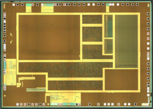
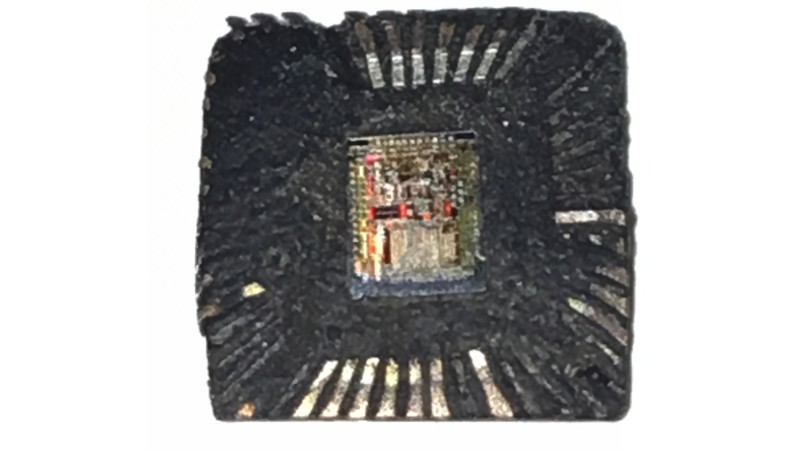
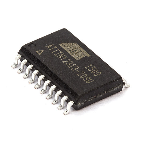
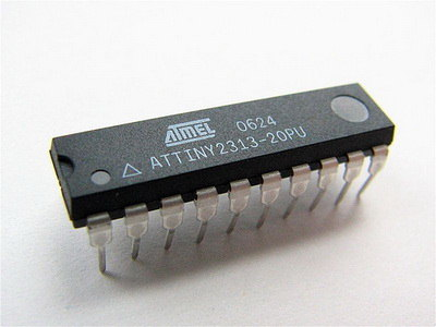
 Attack Chip ATtiny2313 and extract mcu attiny2313 Firmware from flash and eeprom memory in the format of heximal, unlock microcontroller attiny2313 fuse bit by focus ion beam;
Features
· High Performance, Low Power AVR 8-Bit Microcontroller
· Advanced RISC Architecture
– 120 Powerful Instructions – Most Single Clock Cycle Execution
– 32 x 8 General Purpose Working Registers
– Fully Static Operation
– Up to 20 MIPS Throughput at 20 MHz
Data and Non-volatile Program and Data Memories if break mcu pic16f631 flash
– 2/4K Bytes of In-System Self Programmable Flash
· Endurance 10,000 Write/Erase Cycles
– 128/256 Bytes In-System Programmable EEPROM
· Endurance: 100,000 Write/Erase Cycles
Technical Methodology for Firmware Analysis
Our firmware analysis process for ATtiny2313 devices follows a structured, non-destructive methodology. We begin with comprehensive examination of the microcontroller’s configuration, analyzing fuse bit settings and lock bit configurations to understand the specific security implementation. This initial assessment determines the appropriate technical approach for accessing the protected memory contents.
For devices where security features have been enabled, we employ specialized hardware interfaces and signal analysis techniques to establish controlled communication with the microcontroller’s internal systems. This process requires precise timing control and deep understanding of AVR architecture to navigate around protective barriers without triggering permanent lockout mechanisms or damaging the physical device . The goal is to extract the complete firmware image while preserving both the microcontroller’s integrity and the recovered data’s accuracy.
– 128/256 Bytes Internal SRAM
– Programming Lock for Flash Program and EEPROM Data Security
Peripheral Features
– One 8-bit Timer/Counter with Separate Prescaler and Compare Mode
– One 16-bit Timer/Counter with Separate Prescaler, Compare and Capture Modes
– Four PWM Channels
– On-chip Analog Comparator
– Programmable Watchdog Timer with On-chip Oscillator
– USI – Universal Serial Interface
– Full Duplex USART
Special Microcontroller Features
– debugWIRE On-chip Debugging
– In-System Programmable via SPI Port
– External and Internal Interrupt Sources
– Low-power Idle, Power-down, and Standby Modes when Attack mcu pic12f510 program
– Enhanced Power-on Reset Circuit
– Programmable Brown-out Detection Circuit
– Internal Calibrated Oscillator
I/O and Packages
– 18 Programmable I/O Lines
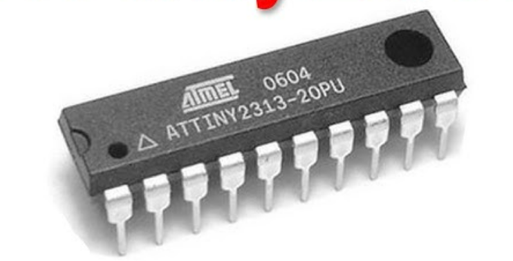
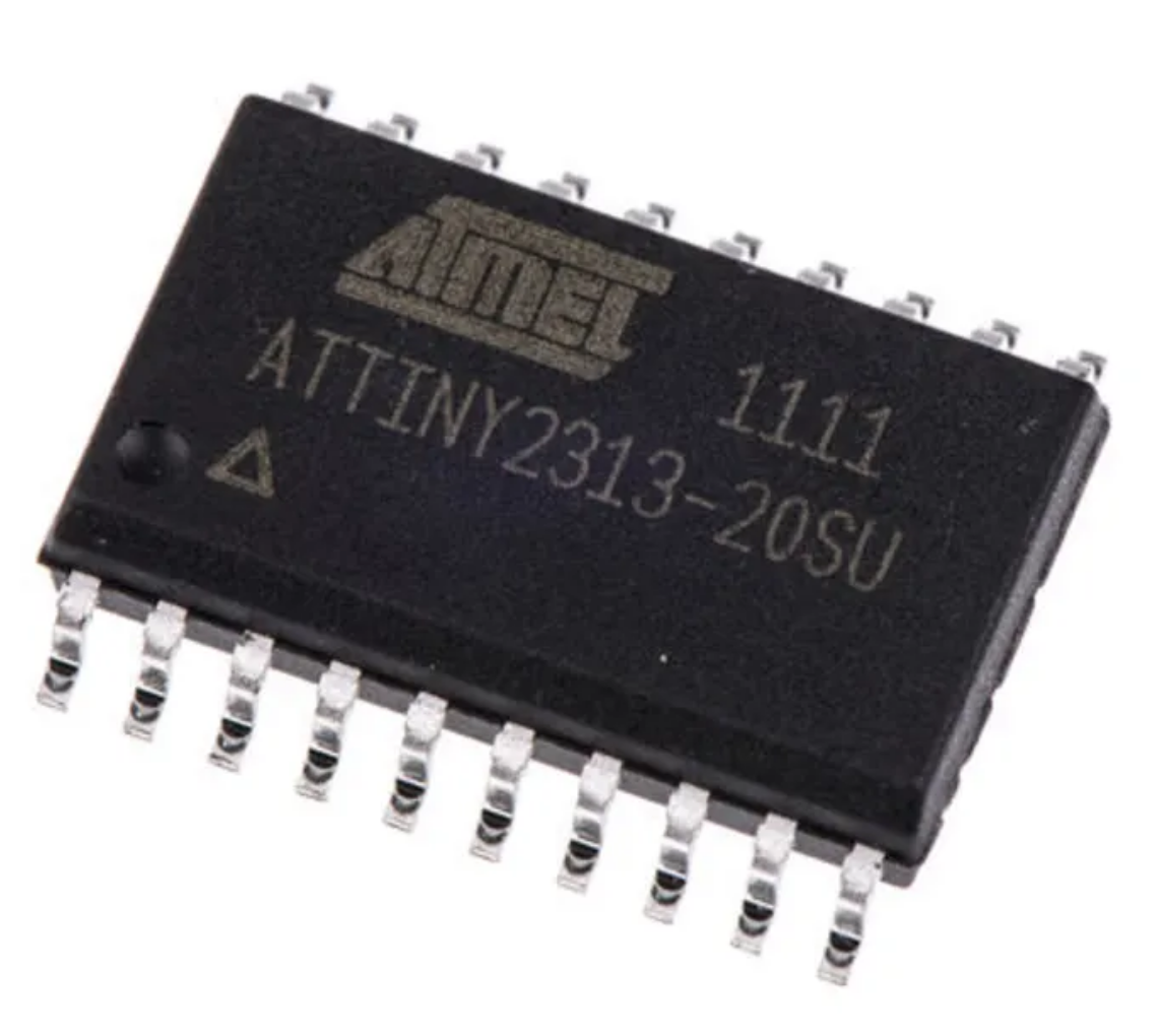
– 20-pin PDIP, 20-pin SOIC, 20-pad MLF/VQFN
Operating Voltage
– 1.8 – 5.5V
Speed Grades
– 0 – 4 MHz @ 1.8 – 5.5V
– 0 – 10 MHz @ 2.7 – 5.5V
– 0 – 20 MHz @ 4.5 – 5.5V
Industrial Temperature Range: -40°C to +85°C
Low Power Consumption
– Active Mode
· 190 µA at 1.8V and 1MHz
– Idle Mode
· 24 µA at 1.8V and 1MHz
– Power-down Mode
· 0.1 µA at 1.8V and +25°C
Firmware Extraction and Binary Recovery
Once access is established, our equipment performs a complete memory read operation, capturing every byte stored within the ATtiny2313’s Flash program memory and EEPROM data sections. This process generates a raw binary file that represents the exact firmware image as originally programmed. For applications requiring specific formats, we convert this binary data into Intel HEX format or other industry-standard file types suitable for analysis or reprogramming.
The extracted binary contains both executable code and configuration data that define the microcontroller’s behavior in its target application. Our technical team processes this raw information to reconstruct the firmware’s logical structure, identifying program sections, data tables, interrupt vectors, and configuration parameters. This transformation creates organized, analyzable files that maintain the functional integrity of the original software.
Applications and Technical Applications
Professional ATtiny2313 firmware analysis serves numerous legitimate engineering purposes. Organizations utilize our services to maintain legacy equipment when original manufacturers no longer support products, to recover from hardware failures where backup firmware is unavailable, to verify the integrity of existing systems, and to understand proprietary implementations for compatibility development.
The recovered firmware documentation provides engineering teams with the technical insights needed to maintain critical systems, develop compatible replacements, or upgrade existing functionality. This capability proves particularly valuable in industrial automation, automotive systems, medical devices, and other applications where long-term equipment reliability depends on access to embedded software.
Conclusion: Responsible Firmware Analysis
Professional firmware analysis for ATtiny2313 microcontrollers represents an essential technical service in today’s complex electronics landscape. Our methodology prioritizes technical precision, device integrity, and ethical compliance, providing legitimate access to secured firmware for authorized engineering purposes. By employing systematic approaches that respect both hardware limitations and intellectual property considerations, we enable continued innovation and maintenance while upholding the highest professional standards.
Recover MCU ATtiny44V Code
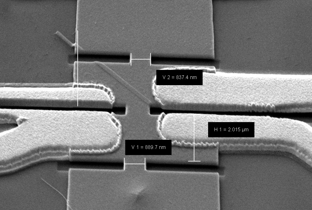
Recover MCU ATtiny44V needs to extract code from attiny44v mcu, using microcontroller unlocking technique to remove the protection over attiny44v;
The ATtiny44v is a low-power CMOS 8-bit microcontroller based on the AVR enhanced RISC architecture. By executing powerful instructions in a single clock cycle, the ATtiny44v achieves throughputs approaching 1 MIPS per MHz allowing the system designer to optimize power consumption versus processing speed when break pic16f715 MCU firmware.
The AVR core combines a rich instruction set with 32 general purpose working registers. All the 32 registers are directly connected to the Arithmetic Logic Unit (ALU), allowing two independent registers to be accessed in one single instruction executed in one clock cycle. The resulting architecture is more code efficient while achieving throughputs up to ten times faster than conventional CISC microcontrollers.
The ATtiny13 provides the following features: 1K byte of In-System Programmable Flash, 64 bytes EEPROM, 64 bytes SRAM, 6 general purpose I/O lines, 32 general purpose working registers, one 8-bit Timer/Counter with compare modes, Internal and External Interrupts, a 4-channel, 10-bit ADC, a programmable Watchdog Timer with internal Oscillator, and three software selectable power saving modes before break pic16f88 MCU.
The Idle mode stops the CPU while allowing the SRAM, Timer/Counter, ADC, Analog Comparator, and Interrupt system to continue functioning. The Power-down mode saves the register contents, disabling all MCU functions until the next Interrupt or Hardware Reset. The ADC Noise Reduction mode stops the CPU and all I/O modules except ADC, to minimize switching noise during ADC conversions.
The device is manufactured using Atmel’s high density non-volatile memory technology. The On-MCU ISP Flash allows the Program memory to be re-programmed In-System through an SPI serial interface, by a conventional non-volatile memory programmer or by an On-MCU boot code running on the AVR core when break pic12ce518 MCU.
The ATtiny13 AVR is supported with a full suite of program and system development tools including: C Compilers, Macro Assemblers, Program Debugger/Simulators, In-Circuit Emulators, and Evaluation kits.
Port B is a 6-bit bi-directional I/O port with internal pull-up resistors (selected for each bit). The Port B output buffers have symmetrical drive characteristics with both high sink and source capability. As inputs, Port B pins that are externally pulled low will source current if the pull-up resistors are activated. The Port B pins are tri-stated when a reset condition becomes active, even if the clock is not running.
 Posted in Recover Chip |
  Tags: recover mcu source archive, recover mcu source binary, recover mcu source code, recover mcu source content, recover mcu source data, recover mcu source eeprom, recover mcu source file, recover mcu source firmware, recover mcu source heximal, recover mcu source information, recover mcu source memory, recover mcu source program |
  Comments Closed
Attack Microcontroller AT88SC0104C Software
We can Attack Microcontroller AT88SC0104C Software, please view below Microcontroller AT88SC0104C features for your reference:
One of a family of nine devices with user memories from 1Kbit to 256Kbit
1Kbit (128-byte) EEPROM user memory
Four 32 byte (256 bit) zones
Self-timed write cycle
Single byte or 16-byte page write mode
Programmable access rights for each zone when Attack Microcontroller
2Kbit configuration zone
· 37-byte OTP area for user-defined codes
· 160-byte area for user-defined keys and passwords
High security features
64-bit mutual authentication protocol (under license of ELVA) when Attack Microcontroller
Encrypted checksum
Stream encryption
Four key sets for authentication and encryption
Eight sets of two 24-bit passwords
Anti-tearing function
Voltage and frequency monitor if Attack Microcontroller
Smart card features
ISO 7816 Class A (5V) or Class B (3V) operation
ISO 7816-3 asynchronous T = 0 protocol (Gemplus® patent) *
Multiple zones, key sets and passwords for multi-application use
Synchronous two-wire serial interface for faster device initialization * before Attack Microcontroller
Programmable 8-byte answer-to-reset register
ISO 7816-2 compliant modules
Embedded application features
Low voltage operation: 2.7V to 5.5V after Attack Microcontroller
Secure nonvolatile storage for sensitive system or user information
Two-wire serial interface
1.0MHz compatibility for fast operation
Standard 8-lead plastic packages, green compliant (exceeds RoHS) when Attack Microcontroller
Same pinout as two-wire Serial EEPROM’s
High reliability if REVERSE ENGINEERING Microcontroller
· Endurance: 100,000 cycles
· Data retention: 10 years
· ESD protection: 4,000V min
Posted in Recover MCU |
Tags: kopieren integrierte Schaltung bin, kopieren integrierte Schaltung code, kopieren integrierte Schaltung data, kopieren integrierte Schaltung eeprom, kopieren integrierte Schaltung hex, kopieren integrierte Schaltung memory, kopieren integrierte Schaltung program |
Comments Closed
Break MCU ATtiny24V Flash
Break MCU ATtiny24V security fuse bit and crack microcontroller attiny24v system against unauthorized reading, extract program from attiny24v mcu Flash and eeprom memory;
The AVR core combines a rich instruction set with 32 general purpose working registers. All the 32 registers are directly connected to the Arithmetic Logic Unit (ALU), allowing two independent registers to be accessed in one single instruction executed in one clock cycle when Break pld palce16v8 software.
The resulting architecture is more code efficient while achieving throughputs up to ten times faster than conventional CISC mcus.
The ATtiny24/44/84 provides the following features: 2/4/8K byte of In-System Programmable Flash, 128/256/512 bytes EEPROM, 128/256/512 bytes SRAM, 12 general purpose I/O lines, 32 general purpose working registers, a 8-bit Timer/Counter with two PWM channels, a 16-bit timer/counter with two PWM channels, Internal and External Interrupts, a 8-channel 10-bit ADC, programmable gain stage (1x, 20x) for 12 differential ADC channel pairs, a programmable Watchdog Timer with internal Oscillator, internal calibrated oscillator, and three software selectable power saving modes if Break pic16c717 mcu program.
The Idle mode stops the CPU while allowing the SRAM, Timer/Counter, ADC, Analog Comparator, and Interrupt system to continue functioning. The Power-down mode saves the register contents, disabling all chip functions until the next Interrupt or Hardware Reset before attack pic16c710 Mcu.
The ADC Noise Reduction mode stops the CPU and all I/O modules except ADC, to minimize switching noise during ADC conversions. In Standby mode, the crystal/resonator Oscillator is running while the rest of the device is sleeping. This allows very fast start-up combined with low power consumption.
The device is manufactured ng Atmel’s high density non-volatile memory technology. The On-chip ISP Flash allows the Program memory to be re-programmed In-System through an SPI serial interface, by a conventional non-volatile memory programmer or by an On-chip boot code running on the AVR core.
The ATtiny24/44/84 AVR is supported with a full suite of program and system development tools including: C Compilers, Macro Assemblers, Program Debugger/Simulators, In-Circuit Emulators, and Evaluation kits. Port B is a 4-bit bi-directional I/O port with internal pull-up resistors (selected for each bit) if recover pic16c74 Mcu code.
The Port B output buffers have symmetrical drive characteristics with both high sink and source capability except PB3 which has the RESET capability. To use pin PB3 as an I/O pin, instead of RESET pin, program (‘0’) RSTDISBL fuse. As inputs, Port B pins that are externally pulled low will source current if the pull-up resistors are activated.
The Port B pins are tri-stated when a reset condition becomes active, even if the clock is not running. Port A is a 8-bit bi-directional I/O port with internal pull-up resistors (selected for each bit). The Port A output buffers have symmetrical drive characteristics with both high sink and source capability.
As inputs, Port A pins that are externally pulled low will source current if the pull-up resistors are activated. The Port A pins are tri-stated when a reset condition becomes active, even if the clock is not running.
Posted in Break IC |
Tags: break mcu encrypted archive, break mcu encrypted binary, break mcu encrypted code, break mcu encrypted content, break mcu encrypted data, break mcu encrypted eeprom, break mcu encrypted file, break mcu encrypted firmware, break mcu encrypted heximal, break mcu encrypted information, break mcu encrypted memory, break mcu encrypted program |
Comments Closed
Break Chip ATmega48PA Firmware
Break Chip ATmega48PA tamper resistance system and readout the firmware from microcontroller atmega48pa flash memory, the mcu atmega48pa fuse bit will be broken when crack it;
· High Performance, Low Power AVR® 8-Bit Microcontroller
· Advanced RISC Architecture
– 131 Powerful Instructions – Most Single Clock Cycle Execution
– 32 x 8 General Purpose Working Registers
– Fully Static Operation
– Up to 20 MIPS Throughput at 20 MHz
– On-chip 2-cycle Multiplier
– 4/8/16/32K Bytes of In-System Self-Programmable Flash progam memory (ATmega48PA/88PA/168PA/328P)
– 256/512/512/1K Bytes EEPROM (ATmega48PA/88PA/168PA/328P)
– 512/1K/1K/2K Bytes Internal SRAM (ATmega48PA/88PA/168PA/328P) if recover pic16f873 chip hex
– Write/Erase Cycles: 10,000 Flash/100,000 EEPROM
– Data retention: 20 years at 85°C/100 years at 25°C(1)
– Optional Boot Code Section with Independent Lock Bits
In-System Programming by On-chip Boot Program
True Read-While-Write Operation
– Programming Lock for Software Security
Peripheral Features
– Two 8-bit Timer/Counters with Separate Prescaler and Compare Mode
– One 16-bit Timer/Counter with Separate Prescaler, Compare Mode, and Capture
Mode
– Real Time Counter with Separate Oscillator before reocver mcu dspic30f6013a firmware
– Six PWM Channels
– 8-channel 10-bit ADC in TQFP and QFN/MLF package
Temperature Measurement
– 6-channel 10-bit ADC in PDIP Package
Temperature Measurement
– Programmable Serial USART
– Master/Slave SPI Serial Interface
– Byte-oriented 2-wire Serial Interface (Philips I2C compatible)
– Programmable Watchdog Timer with Separate On-chip Oscillator
– On-chip Analog Comparator
– Interrupt and Wake-up on Pin Change
Special Microcontroller Features
– Power-on Reset and Programmable Brown-out Detection if Break mcu at89c513a Chip
– Internal Calibrated Oscillator
– External and Internal Interrupt Sources
– Six Sleep Modes: Idle, ADC Noise Reduction, Power-save, Power-down, Standby, and Extended Standby I/O and Packages
– 23 Programmable I/O Lines
– 28-pin PDIP, 32-lead TQFP, 28-pad QFN/MLF and 32-pad QFN/MLF
Operating Voltage:
– 1.8 – 5.5V for ATmega48PA/88PA/168PA/328P
Temperature Range:
– -40°C to 85°C
Speed Grade:
– 0 – 20 MHz @ 1.8 – 5.5V
Low Power Consumption at 1 MHz, 1.8V, 25°C for ATmega48PA/88PA/168PA/328P:
Programmable Flash
ATmega48PA
ATmega88PA
ATmega168PA
ATmega328P
– Active Mode: 0.2 mA
– Power-down Mode: 0.1 µA
– Power-save Mode: 0.75 µA (Including 32 kHz RTC) before Break Chip
Break Microcontroller ATtiny24 Code
Break Microcontroller ATtiny24 is a process to unlock mcu attiny24’s fuse bit and then extract code from microprocessor attiny24 flash and eeprom memory for MCU cloning;
Features
High Performance, Low Power AVR® 8-Bit Microcontroller
Advanced RISC Architecture
– 120 Powerful Instructions – Most Single Clock Cycle Execution
– 32 x 8 General Purpose Working Registers
– Fully StatMicrocontroller Operation
Non-volatile Program and Data Memories
– 2/4/8K Byte of In-System Programmable Program Memory Flash (ATtiny24/44/84)
Endurance: 10,000 Write/Erase Cycles
– 128/256/512 Bytes In-System Programmable EEPROM (ATtiny24/44/84)
Endurance: 100,000 Write/Erase Cycles
– 128/256/512 Bytes Internal SRAM (ATtiny24/44/84)
– Programming Lock for Self-Programming Flash Program and EEPROM Data Security before decrypt ic flash memory
Peripheral Features
– Two Timer/Counters, 8- and 16-bit counters with two PWM Channels on both
– 10-bit ADC
8 single-ended channels
12 differential ADC channel pairs with programmable gain (1x, 20x) Temperature Measurement
– Programmable Watchdog Timer with Separate On-chip Oscillator
– On-chip Analog Comparator
– Universal Serial Interface
Special MMicrocontrollerrocontroller Features
– debugWIRE On-chip Debug System
– In-System Programmable via SPI Port
– External and Internal Interrupt Sources
– Pin Change Interrupt on 12 pins
– Low Power Idle, ADC Noise Reduction, Standby and Power-down Modes
– Enhanced Power-on Reset Circuit
– Programmable Brown-out Detection Circuit
– Internal Calibrated Oscillator
– On-chip Temperature Sensor I/O and Packages
– 14-pin SOMICROCONTROLLER, PDIP and 20-pin QFN/MLF: Twelve Programmable I/O Lines
Operating Voltage:
– 1.8 – 5.5V for ATtiny24V/44V/84V
– 2.7 – 5.5V for ATtiny24/44/84
Speed Grade
– ATtiny24V/44V/84V: 0 – 4 MHz @ 1.8 – 5.5V, 0 – 10 MHz @ 2.7 – 5.5V
– ATtiny24/44/84: 0 – 10 MHz @ 2.7 – 5.5V, 0 – 20 MHz @ 4.5 – 5.5V
Industrial Temperature Range
Low Power Consumption
Preliminary Summary
– Active Mode:
1 MHz, 1.8V: 380 µA
– Power-down Mode:
1.8V: 100 nA
The ATtiny24/44/84 is a low-power CMOS 8-bit Microcontroller based on the AVR enhanced RISC architecture. By executing powerful instructions in a single clock cycle, the ATtiny24/44/84 achieves throughputs approaching 1 MIPS per MHz allowing the system designer to optimize power consumption versus processing speed when Break MICROCONTROLLER.
Posted in Reverse Engineer Microcontroller |
Tags: break microcontroller encrypted archive, break microcontroller encrypted binary, break microcontroller encrypted code, break microcontroller encrypted content, break microcontroller encrypted data, break microcontroller encrypted eeprom, break microcontroller encrypted file, break microcontroller encrypted firmware, break microcontroller encrypted heximal, break microcontroller encrypted information, break microcontroller encrypted memory, break microcontroller encrypted program |
Comments Closed
Recover MCU ATmega168PV Code
Recover MCU ATmega168PV Code from locked flash memory, fuse bit of microcontroller atmega168pv will be cracked and heximal file in the program and data memory will be extracted from chip atmega168pv;
An EEPROM data corruption can be caused by two situations when the voltage is too low. First, a regular write sequence to the EEPROM requires a minimum voltage to operate correctly. Secondly, the CPU itself can execute instructions incorrectly, if the supply voltage is too low when Recover MCU.
EEPROM data corruption can easily be avoided by following this design recommendation: Keep the AVR RESET active (low) during periods of insufficient power supply voltage. This can be done by enabling the internal Brown-out Detector (BOD). If the detection level of the internal BOD does not match the needed detection level, an external low VCC reset Protection circuit can be used if Recover MCU.
If a reset occurs while a write operation is in progress, the write operation will be completed provided that the power supply voltage is sufficient. The I/O space definition of the ATmega48/88/168 is shown in ”Register Summary” on page 342. All ATmega48/88/168 I/Os and peripherals are placed in the I/O space. All I/O locations may be accessed by the LD/LDS/LDD and ST/STS/STD instructions, transferring data between the 32 general purpose working registers and the I/O space. I/O Registers within the address range 0x00 – 0x1F are directly bit-accessible using the SBI and CBI instructions. In these registers, the value of single bits can be checked by using the SBIS and SBIC instructions before break atmega128pa MCU.
Refer to the instruction set section for more details. When using the I/O specific commands IN and OUT, the I/O addresses 0x00 – 0x3F must be used. When addressing I/O Registers as data space using LD and ST instructions, 0x20 must be added to these addresses. The ATmega48/88/168 is a complex MCU with more peripheral units than can be supported within the 64 location reserved in Opcode for the IN and OUT instructions.
For the Extended I/O space from 0x60 – 0xFF in SRAM, only the ST/STS/STD and LD/LDS/LDD instructions can be used. For compatibility with future devices, reserved bits should be written to zero if accessed. Reserved I/O memory addresses should never be written. Some of the Status Flags are cleared by writing a logical one to them. Note that, unlike most other AVRs, the CBI and SBI instructions will only operate on the specified bit, and can therefore be used on registers containing such Status Flags. The CBI and SBI instructions work with registers 0x00 to 0x1F only when break atmega168a MCU.
The I/O and peripherals control registers are explained in later sections. The ATmega48/88/168 contains three General Purpose I/O Registers. These registers can be used for storing any information, and they are particularly useful for storing global variables and Status Flags. General Purpose I/O Registers within the address range 0x00 – 0x1F are directly bit-accessible using the SBI, CBI, SBIS, and SBIC instructions.
The EEPROM Read Enable Signal EERE is the read strobe to the EEPROM. When the correct address is set up in the EEAR Register, the EERE bit must be written to a logic one to trigger the EEPROM read. The EEPROM read access takes one instruction, and the requested data is available immediately. When the EEPROM is read, the CPU is halted for four cycles before the next instruction is executed.
The user should poll the EEPE bit before starting the read operation. If a write operation is in progress, it is neither possible to read the EEPROM, nor to change the EEAR Register. The calibrated Oscillator is used to time the EEPROM accesses. Table 6-2 lists the typical programming time for EEPROM access from the CPU.
The following code examples show one assembly and one C function for writing to the EEPROM. The examples assume that interrupts are controlled (e.g. by disabling interrupts globally) so that no interrupts will occur during execution of these functions. The examples also assume that no Flash Boot Loader is present in the software. If such code is present, the EEPROM write function must also wait for any ongoing SPM command to finish when Recover MCU.
Copy IC PIC12C509A Binary
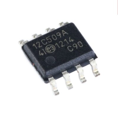
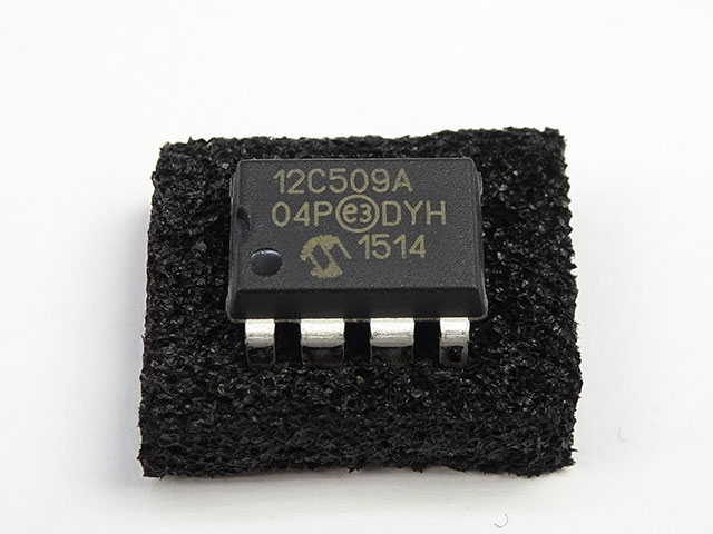
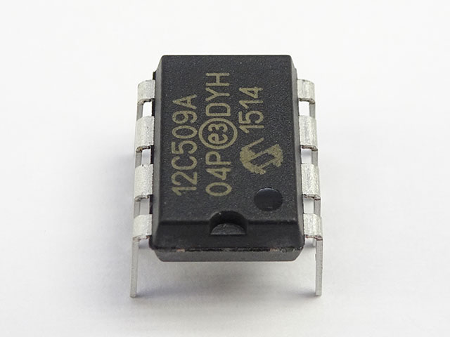
When clients need to Copy IC PIC12C509A Binary, they often face the challenge of dealing with a protected and deeply embedded 8-bit microcontroller widely used in industrial controls, small consumer devices, automotive sensors, smart tools, and custom electronic modules. The PIC12C509A’s compact design and secured memory structure make it reliable for manufacturers—but difficult for anyone who needs to retrieve, clone, or duplicate the original program or firmware stored inside it.
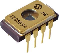
Our engineering team specializes in helping customers attack, break, and technically hack highly encrypted and locked PIC12C509A devices. Through controlled decapsulation, advanced micro-probing, and non-destructive analysis, we can decode and extract the binary, heximal, or source code-level data from the internal flash, EEPROM, or program memory. This allows us to rebuild the original file, archive, or program structure even when the chip’s protective mechanisms are fully enabled.
Copy IC PIC12C509A Binary content after unlock mcu pic12c509a flash and eeprom memory, extract program and data from microcontroller pic12c509a memory in the format of heximal;
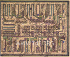
PIC12C5XX memory is organized into program memory and data memory. For devICes with more than 512 bytes of program memory, a paging scheme is used.
Program memory pages are accessed using one STATUS register bit. For the PIC12C509, PIC12C509A, PICCR509A and PIC12CE519 with a data memory register file of more than 32 registers, a banking scheme is used. Data memory banks are accessed using the File Select Register (FSR) when break mcu pic10f200 memory.
The PIC12C5XX devICes have a 12-bit Program Counter (PC) capable of addressing a 2K x 12 program memory space. Only the first 512 x 12 (0000h-01FFh) for the PIC12C508, PIC12C508A and PIC12CE518 and 1K x 12 (0000h-03FFh) for the PIC12C509, PIC12C509A, PIC12CR509A, and PIC12CE519 are physICally implemented.
Refer to Figure 4-1. Accessing a location above these boundaries will cause a wrap around within the first 512 x 12 space (PIC12C508, PIC12C508A and PIC12CE518) or 1K x 12 space (PIC12C509, PIC12C509A, PIC12CR509A and PIC12CE519). The effective reset vector is at 000h, (see Figure 4-1). Location 01FFh (PIC12C508, PIC12C508A and PIC12CE518) or location 03FFh (PIC12C509, PIC12C509A, PIC12CR509A and PIC12CE519) contains the internal clock oscillator calibration value. This value should never be overwritten when break microcontroller pic16f886 software memory.
As a program instruction is executed, the Program Counter (PC) will contain the address of the next program instruction to be executed. The PC value is increased by one every instruction cycle, unless an instruction changes the PC.
For a GOTO instruction, bits 8:0 of the PC are provided by the GOTO instruction word. The PC Latch (PCL) is mapped to PC<7:0>. Bit 5 of the STATUS register provides page information to bit 9 of the PC (Figure 4- 8).For a CALL instruction, or any instruction where the PCL is the destination before Copy IC, bits 7:0 of the PC again are provided by the instruction word. However, PC<8> does not come from the instruction word, but is always cleared (Figure 4-8).
Instructions where the PCL is the destination, or Modify PCL instructions, include MOVWF PC, ADDWF PC, and BSF PC,5. The Program Counter is set upon a RESET, whICh means that the PC addresses the last location in the last page i.e., the oscillator calibration instruction. After executing MOVLW XX, the PC will roll over to location 00h, and begin executing user code.
The STATUS register page preselect bits are cleared upon a RESET, whICh means that page 0 is pre-selected. Therefore, upon a RESET, a GOTO instruction will automatICally cause the program to jump to page 0 until the value of the page bits is altered.
Why Clients Need This Service
Manufacturers and repair centers often require binary duplication for:
- Rebuilding obsolete or discontinued products
- Restoring damaged units when no backup exists
- Ensuring compatibility across cloned or redesigned PCB modules
- Migrating legacy firmware into newer embedded platforms
- Conducting failure analysis or system re-engineering
By enabling accurate firmware recovery, we help customers extend product life cycles, reduce downtime, and maintain operational continuity.
Difficulties & Why Expertise Matters
The PIC12C509A features strong protective code-security fuses, making direct extraction impossible through standard tools. Micro-level silicon analysis, timing-based fault techniques, and detailed memory reconstruction are required, and only an experienced specialist team can perform the process reliably without damaging the chip.
Your Trusted Technical Partner
Our service delivers fast, accurate, and confidential PIC12C509A binary extraction with full technical support. Whether your goal is cloning, duplicating, or simply retrieving critical embedded data, we provide a safe, professional solution tailored to demanding industrial requirements.
Break IC ATmega128A Firmware
Break IC ATmega128A to restore the Firmware from atmel microcontroller atmega128a flash and eeprom memory, the mcu atmega128a heximal file reading must be taken after the fuse bit has been reset;
The Atmel QTouch Library provides a simple to use solution to realize touch sensitive interfaces on most Atmel AVR microcontrollers. The QTouch Library includes support for the QTouch and QMatrix acquisition methods. Touch sensing can be added to any application by linking the appropriate Atmel QTouch Library for the AVR Microcontroller. This is done by using a simple set of APIs to define the touch channels and sensors, and then calling the touch sensing API’s to retrieve the channel information and determine the touch sensor states.
The QTouch Library is FREE and downloadable from the Atmel website at the following location: www.atmel.com/qtouchlibrary. For implementation details and other information, refer to the Atmel QTouch Library User Guide – also available for download from the Atmel website. This datasheet contains simple code examples that briefly show how to use various parts of the device.
These code examples assume that the part specific header file is included before compilation. Be aware that not all C compiler vendors include bit definitions in the header files and interrupt handling in C is compiler dependent. Please confirm with the C compiler documentation for more details. For I/O registers located in extended I/O map, “IN”, “OUT”, “SBIS”, “SBIC”, “CBI”, and “SBI” instructions must be replaced with instructions that allow access to extended I/O. Typically “LDS” and “STS” combined with “SBRS”, “SBRC”, “SBR”, and “CBR”.
The Atmel QTouch Library provides a simple to use solution to realize touch sensitive interfaces on most Atmel AVR microcontrollers. The QTouch Library includes support for the QTouch and QMatrix acquisition methods. Touch sensing can be added to any application by linking the appropriate Atmel QTouch Library for the AVR Microcontroller.
This is done by using a simple set of APIs to define the touch channels and sensors, and then calling the touch sensing API’s to retrieve the channel information and determine the touch sensor states. The QTouch Library is FREE and downloadable from the Atmel website at the following location: www.atmel.com/qtouchlibrary. For implementation details and other information, refer to the Atmel QTouch Library User Guide – also available for download from the Atmel website if attacking mcu memory code.
Recover Microcontroller PIC16C62B Eeprom
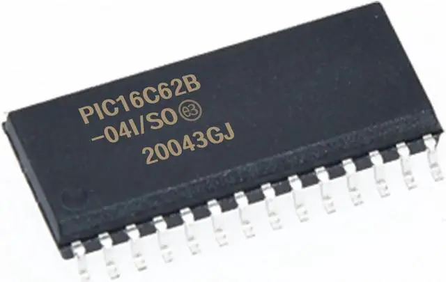
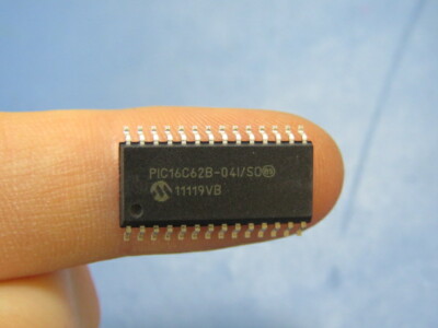
When a device relies on the Microchip PIC16C62B for control and configuration, the small but critical EEPROM and flash areas often hold calibration tables, configuration data, or archived program fragments that are essential to operation. Our service, searchable under the keyword Recover Microcontroller PIC16C62B Eeprom, helps authorized owners and technicians safely open, readout, restore, and duplicate the firmware/binary/heximal and small nonvolatile memory regions of these controllers. We focus on lawful, confidential recovery that returns usable program archives without disclosing methods to bypass manufacturer protections.
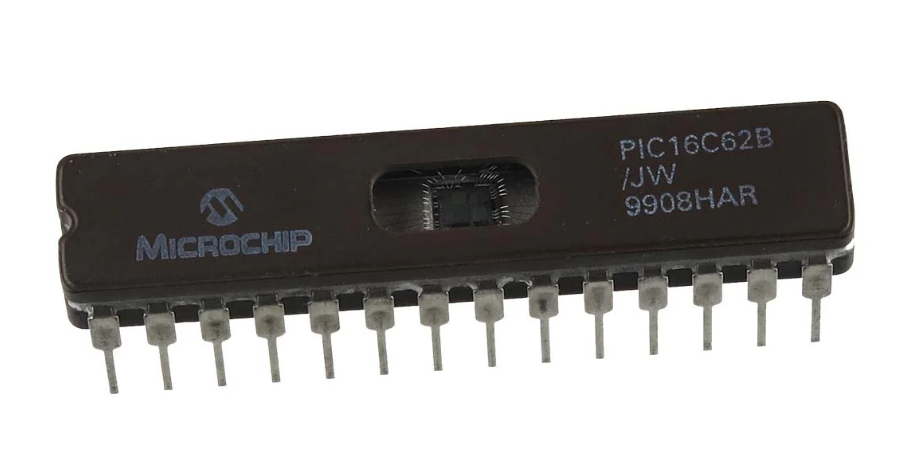
Recover Microcontroller PIC16C62B Eeprom data and extract mcu pic16c62b code from flash and eeprom memory, the secured firmware can be readount from mcu pic16c62b microprocessor memory;
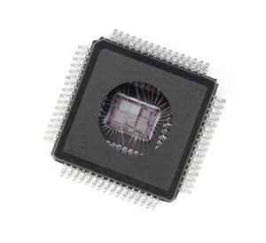
We can recover MCU PIC16C62B Eeprom, please view the Microcontroller PIC16C62B features for your reference:
Microcontroller Core Features: · High-performance RISC CPU · Only 35 single word instructions to learn · All single cycle instructions except for program branches, which are two cycle·
Operating speed: DC – 20 MHz clock input DC – 200 ns instruction cycle · 2K x 14 words of Program Memory, 128 x 8 bytes of Data Memory (RAM) ·
Devices with PIC16C62B controllers are often legacy or long-lived products. Valid reasons to request recovery include the need to restore corrupted EEPROM after failures, copy configuration files for authorized spares, clone settings for production runs, or duplicate archived data before servicing. Recovering a verified binary or heximal image of the EEPROM can avoid lengthy software rewrites and shorten downtime.
Typical applications of PIC16C62B
The PIC16C62B’s modest feature set and reliable I/O make it suitable for many industries:
- Consumer appliances and simple household electronics.
- Industrial sensors and controllers for basic automation tasks.
- Instrumentation and measurement devices that store small data archives.
- Aftermarket and hobbyist systems where a compact embedded controller is sufficient.
Because these applications frequently store system-critical parameters in EEPROM, the data is often treated as a protected, locked, or secured asset.
Eight level deep hardware stack ·
Direct, indirect, and relative addressing modes ·
Power-on Reset (POR) · Power-up Timer (PWRT) and Oscillator Start-up Timer (OST)·
Watchdog Timer (WDT) with its own on-microcontroller RC oscillator for reliable operation · Brown-out detection circuitry for Brown-out Reset (BOR) · Programmable code-protection · Power saving SLEEP mode · Selectable oscillator options · Low-power, high-speed CMOS EPROM technology·
Fully static design · In-Circuit Serial Programming (ICSP) · Wide operating voltage range: 2.5V to 5.5V · High Sink/Source Current 25/25 mA · Commercial, Industrial and Extended temperature ranges · Low-power consumption: – < 2 mA @ 5V, 4 MHz – 22.5 µA typical @ 3V, 32 kHz when copy pic16f684 Microcontroller firmware – < 1 µA typical standby current Peripheral Features: · Timer0: 8-bit timer/counter with 8-bit prescaler · Timer1: 16-bit timer/counter with prescaler, can be incremented during sleep via external crystal/clock · Timer2: 8-bit timer/counter with 8-bit period register, prescaler and postscaler · Capture, Compare, PWM module · Capture is 16-bit, max. resolution is 12.5 ns, Compare is 16-bit, max. resolution is 200 ns, PWM maximum resolution is 10-bit · 8-bit multi-channel Analog-to-Digital converter · Synchronous Serial Port (SSP) with Enhanced SPI and I2C
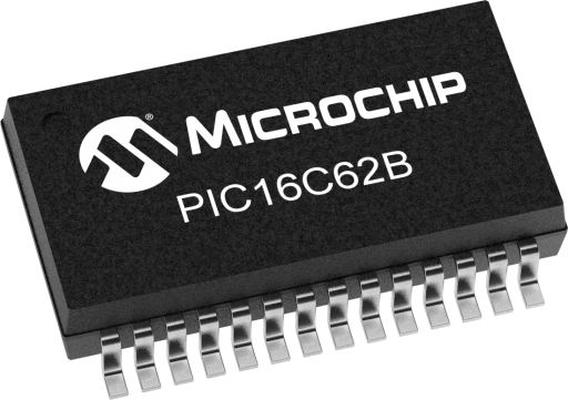
The PIC16C62B integrates limited program memory alongside EEPROM for persistent settings, plus basic analog/digital peripherals. These constrained resources mean key configuration files and calibration tables are concentrated in small memory regions — making careful extraction essential. The chip’s architecture affects how source code (if available) and program data are represented in the raw binary/heximal dumps.
General idea of our approach (non-actionable)
We begin every engagement with ownership verification and a risk assessment. Our work emphasizes non-destructive procedures to obtain a reliable memory archive. After a validated readout, we produce checked heximal or binary dumps and provide high-level annotated summaries that help engineers interpret recovered data. We do not publish or provide step-by-step techniques to crack, hack, or illegally decode protections — our focus is on authorized recovery, unlock, and restoration for legitimate purposes.
Purpose and benefits for end users
Clients using this service can expect faster recovery of device functionality, secure backups of previously inaccessible EEPROM, and the ability to copy or clone settings for authorized production or maintenance. Recovered program files and archives support debugging, testing, migration to replacement hardware, and continuity for legacy systems — saving time and reducing redevelopment costs.
Common difficulties and limitations
Challenges may include partial data corruption, variant device revisions with different memory maps, or layered protective settings that limit full reconstruction. In many recoveries, the deliverable is a validated binary/heximal archive and assembly-level annotations rather than full, human-readable source code. We always communicate feasibility, likely outcomes, and limitations before proceeding.
Ethics, authorization & confidentiality
All projects require proof of ownership or explicit authorization and are governed by confidentiality agreements. We do not assist with unauthorized copying or distribution of copyrighted or safety-critical firmware. Our goal is to help rightful owners recover, restore, and maintain their embedded systems safely and legally.
If you need to Recover Microcontroller PIC16C62B Eeprom for authorized recovery, maintenance, or archival purposes, our experienced team offers secure, professional support to retrieve and document your embedded firmware and data while protecting your IP and operational continuity.