Posts Tagged ‘recover mcu source heximal’
 Recover MCU ATtiny4313A Code
 August 20th, 2010 |
 Author:
Recover MCU ATtiny4313A Code from embedded memory, the tamper resistance system of microcontroller attiny4313a will be unlocked and code include flash program and eeprom data will be extracted from attiny4313a memory;
The ATtiny2313A/4313 provides the following features: 2/4K bytes of In-System Programmable Flash, 128/256 bytes EEPROM, 128/256 bytes SRAM, 18 general purpose I/O lines, 32 general purpose working registers, a single-wire Interface for On-mcu Debugging, two flexible Timer/Counters with compare modes, internal and external interrupts, a serial programmable USART, Universal Serial Interface with Start Condition Detector, a programmable Watchdog Timer with internal Oscillator, and three software selectable power saving modes.
The Idle mode stops the CPU while allowing the SRAM, Timer/Counters, and interrupt system to continue functioning. The Power-down mode saves the register contents but freezes the Oscillator, disabling all other mcu functions until the next interrupt or hardware reset.
In Standby mode, the crystal/resonator Oscillator is running while the rest of the device is sleeping. This allows very fast start-up combined with low-power consumption. The device is manufactured using Atmel’s high density non-volatile memory technology before attacking Mcu protection.
The On-mcu ISP Flash allows the program memory to be reprogrammed In-System through an SPI serial interface, or by a conventional non-volatile memory programmer.
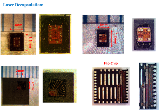
By combining an 8-bit RISC CPU with In-System Self-Programmable Flash on a monolithic mcu, the Atmel ATtiny2313A/4313 is a powerful microcontroller that provides a highly flexible and cost effective solution to many embedded control applications.
The ATtiny2313A/4313 AVR is supported with a full suite of program and system development tools including: C Compilers, Macro Assemblers, Program Debugger/Simulators, In-Circuit Emulators, and Evaluation kits.
This documentation contains simple code examples that briefly show how to use various parts of the device. These code examples assume that the part specific header file is included before compilation. Be aware that not all C compiler vendors include bit definitions in the header files and interrupt handling in C is compiler dependent before attack st62t15c6 Mcu firmware.
Please confirm with the C compiler documentation for more details.
For I/O Registers located in the extended I/O map, “IN”, “OUT”, “SBIS”, “SBIC”, “CBI”, and “SBI” instructions must be replaced with instructions that allow access to extended I/O. Typically, this means “LDS” and “STS” combined with “SBRS”, “SBRC”, “SBR”, and “CBR”.
Note that not all AVR devices include an extended I/O map.
For compatibility with future devices, reserved bits should be written to zero if accessed. Reserved I/O memory addresses should never be written.
I/O Registers within the address range 0x00 – 0x1F are directly bit-accessible using the SBI and CBI instructions. In these registers, the value of single bits can be checked by using the SBIS and SBIC instructions.
Some of the status flags are cleared by writing a logical one to them. Note that, unlike most other AVRs, the CBI and SBI instructions will only operate on the specified bit, and can therefore be used on registers containing such status flags.
The CBI and SBI instructions work with registers 0x00 to 0x1F only;
When using the I/O specific commands IN and OUT, the I/O addresses 0x00 – 0x3F must be used. When addressing I/O
Registers as data space using LD and ST instructions, 0x20 must be added to these addresses.
 Posted in Recover Chip |
 Tags: recover mcu source archive, recover mcu source binary, recover mcu source code, recover mcu source content, recover mcu source data, recover mcu source eeprom, recover mcu source file, recover mcu source firmware, recover mcu source heximal, recover mcu source information, recover mcu source memory, recover mcu source program |
 Comments Closed
ATtiny2313A: Three Ways to Name the Silicon, and Only One Is Stamped on It
A trailing letter is the least dramatic change in a part number and the one that causes the most confusion in a recovery. It does not normally mean a different memory size or a different pinout. It marks a revision: the same design with corrected or improved silicon behind it, sometimes with a wider specification and almost always with its own errata list.
For the person holding the part, that creates a problem with three separate answers. What the package says, what the interface reports, and what the calibration value implies are three different statements about identity, and they do not have to agree.
What a revision letter changes and what it does not
Across this family the storage map and the peripheral set stay fixed: 2 KB of flash, 128 bytes of SRAM, 128 bytes of EEPROM, twenty pins, a USART, an SPI port, a universal serial interface, two timers, an analogue comparator. Code written for one revision runs on the other, because the instruction set and the register map are the same.
What moves is the specification envelope and the defect list. Supply range, maximum frequency at a given voltage, current consumption, the behaviour of a peripheral under a corner condition — these are the things a revision adjusts, and they are exactly the things a fuse configuration encodes. That is the practical consequence: a fuse map copied from a non-A device onto an A device may put the newer part outside its specified operating point even though every bit is a legal bit.
| property | same across revisions | may differ |
|---|---|---|
| flash, SRAM, EEPROM size | yes | — |
| pinout and package | yes | — |
| instruction set | yes | — |
| signature bytes | — | possible |
| oscillator calibration | — | yes, per device and per revision |
| fuse defaults and safe limits | — | yes |
| errata | — | yes |
The signature answers a narrower question than people expect
The three signature bytes report the manufacturer, the family and the memory class. They are read with a dedicated command that does not consume a flash address, which makes them the cheapest identity check available and the first thing to obtain.
What they do not report is the revision in any reliable form. Two devices built from different masks can return the same signature, and the same part number from two production runs can differ in behaviour without differing in signature. So a matching signature proves the interface works and the family is right. It does not prove the marking is honest.
The calibration value is the per-device fingerprint
Every one of these parts is calibrated at test, and the result is stored in a row that is separate from the flash array. That value tunes the internal oscillator, and because it is measured rather than assigned, it varies from device to device within a distribution set by the process.
Two uses follow. The first is functional: an image restored onto a different physical part inherits the donor’s calibration unless the row is rewritten, and the timing consequences range from negligible to fatal depending on whether the design depends on the internal oscillator for a communication rate.
The second is forensic. A batch of genuine parts from one production period has calibration values clustered in a predictable band. A part whose marking says one revision, whose signature says the family, and whose calibration value sits far outside the band for that revision is worth a second look — that combination is characteristic of remarked or refurbished material, which is common in the second-hand market this family ends up in.
The marking is a claim, not a measurement
Laser marking is applied after test and can be removed and reapplied. On a twenty-pin plastic package the operation is not difficult, and the economic incentive is real because the A revision often trades at a different price from the older part.
That does not make every package suspect. It does mean the marking should be treated as the weakest of the three sources rather than the primary one, and that a report which records only the marking is recording the customer’s belief rather than the silicon’s answer.
Reading order for an identity dispute
When the question is specifically «which revision is this», the sequence that settles it without destroying evidence:
- Read the signature. Establish that the interface works and the family is correct.
- Read the fuse and lock bytes as found. They state the operating point the device was configured for, and comparing them against the defaults for the claimed revision is informative.
- Read the calibration row. Compare against the expected band.
- Read the flash, if the lock state allows it, and check the oscillator setup in the initialisation code. A build that programs the divider or selects an external clock is telling you what it expected the part to be.
- Only then compare against the marking.
Steps 1 to 3 are non-destructive. Step 4 may require the erase, so it comes after the decision about whether the flash contents are needed.
What the recovery returns
For a heximal-level job the deliverable is the flash image with the correct length for a 2 KB array, the EEPROM as a separate file, the signature, the calibration value and the fuse and lock state as read, and a disassembly annotated with the register configuration the image assumes.
Recording the calibration value is not decoration. It is the only per-device datum in the set, it cannot be reconstructed from the image, and a customer who later moves the image to another unit needs it to restore the timing the design was built around.
The unsigned variant’s own behaviour under erase is covered in ATtiny2313 code recovery. Where the same package carries 4 KB, ATtiny4313 code recovery follows the migration. The same identification discipline applied to a part with an ambiguous suffix appears in ATtiny48V firmware recovery.
FAQ
Does the A suffix mean more memory? No. The array size is unchanged across the revisions of this part; the suffix marks silicon revision and with it the specification envelope.
Can a fuse map be copied between revisions? The bits will be accepted, but the resulting operating point may be outside the newer part’s specification. Fuse maps belong to a part, not to a family.
Why does the calibration value matter if the code runs? It sets the internal oscillator. Code that runs at the wrong frequency may still execute, and still fail every timing-sensitive function it performs.
Conclusion
Identity on a revised part is a three-way question with three partial answers: the marking states a claim, the signature confirms a family, and the calibration value places a specific device in a production distribution. Read all three, in that order of reliability rather than the order printed on the box, and the revision question stops being a matter of opinion.
Posted in Recover Chip |
Tags: recover mcu source archive, recover mcu source bin, recover mcu source code, recover mcu source content, recover mcu source data, recover mcu source eeprom, recover mcu source file, recover mcu source firmware, recover mcu source heximal, recover mcu source information, recover mcu source memory, recover mcu source program |
Comments Closed
ATtiny44V: Clock Fuses, Start-Up Delay, and a Device That Will Not Talk
A microcontroller needs a clock before it can do anything, including answer a programmer. On this family the clock source is chosen by fuse bits, and the choices include sources that do not exist on a bare socket: a crystal that is not fitted, an external clock that nothing is driving, a resonator that was on the production board and is not on your adapter.
The symptom is a part that draws current, sits quietly, and refuses every command. That is the same symptom as a damaged die, and the fuse byte is what separates them.
The clock options and their failure modes
| Selection | What it needs | Why it fails on a socket |
|---|---|---|
| Internal RC, 8 MHz | nothing | It does not fail; this is the safe default |
| Internal RC, divided | nothing | Works, but slow; the interface answers slowly |
| Low-frequency crystal | a 32 kHz crystal fitted | No crystal, no clock, no response |
| Full-swing crystal | a crystal plus load capacitors | No crystal, no response |
| External clock | a clock signal on a pin | Nothing driving the pin, no response |
The last three rows are the trap. A production board supplies the crystal; a programming adapter usually does not. The part is not locked, not damaged, and not empty — it is simply waiting for a clock that is not there.
Why the start-up delay makes it worse
Fuse bits also select how long the part waits after power-on before releasing the reset. The longest settings exist for crystals that need time to stabilise. On a socket with no crystal, the part waits out the full delay and then runs from a clock that never arrives.
The observable effect is a few tens of milliseconds of complete silence, then still nothing. On an automated programmer with a short timeout, the failure appears as “no device” rather than “device not ready”, and the diagnosis goes in the wrong direction.
Lowering the programmer’s timeout makes the problem worse, which is worth knowing because the instinct is to make the tool faster.
The diagnostic that settles it
Two measurements, in order.
Measure the clock pin. On a part configured for an external clock, the clock input pin should show activity if something is driving it. Nothing there means nothing is driving it.
Read the fuse byte over whichever interface still works. This is the decisive step, and it usually works: the fuse byte is readable in programming mode even when the part has no usable clock, because the programming interface supplies its own timing. A fuse byte that selects a crystal on a socket with no crystal is the answer.
If the fuse read also fails, the situation is genuinely different — an interface problem, not a clock problem — and that is a distinct investigation.
How a device gets into this state
Three routes, all common:
A production build configured for a crystal that the design later removed, with the fuse change never made. A prototype configured for an external clock from a signal generator and shipped that way. A part moved from a working board to a bare adapter by someone who did not check.
In every case the configuration is real, deliberate at the time, and wrong for the current context. None of them is damage.
Recovering a part with a bad clock setting
Once the fuse byte is known, the path is short. Enter programming mode, which does not depend on the target clock, and rewrite the clock selection to the internal RC source. Then the part runs, and the normal read sequence applies.
Two cautions. Changing the clock fuse requires care: the part must be running from a source that exists during the write, and losing the clock mid-write is one of the few ways to leave a device in an awkward state. The internal RC is the safe target precisely because it always exists.
And rewriting a fuse is not reading memory. It does not clear the lock bits and it does not reveal the contents. It only makes the part runnable, which is a precondition for everything else.
The V suffix in this context
The low-voltage grade extends the supply range downward, which interacts with the clock selection: at a low supply the maximum frequency falls, and a part configured to run fast at a voltage that no longer supports it will misbehave in ways that look like a clock fault.
That is a real design constraint and it is invisible from outside. If a device works on a bench supply and fails in its product, the supply and the clock setting are one question, not two.
Related notes
- ATtiny44 and the debug interface — reading behaviour once the part runs.
- ATtiny24V and the debug fuse — the other fuse that produces silence.
- ATmega168PV and the calibration byte — why the internal RC needs trimming at all.
FAQ
Can the fuse byte be read with no clock? Yes, in programming mode. The interface provides its own timing, which is why the fuse read is the decisive diagnostic.
Does a missing crystal damage the part? No. The part waits and does nothing.
Can the clock fuse be changed without erasing? Yes. Fuse writes are independent of the flash array, and the lock bits are unaffected.
Is the internal RC accurate enough to run from? It is accurate enough to boot and communicate. Firmware that depends on precise timing will need either trimming or an external source.
Conclusion
Silence from a small AVR has several causes, and the clock fuse is the cheapest to rule out. If the part is configured for a crystal that is not on the socket, it is behaving correctly and the only problem is context. Reading the fuse byte takes seconds and prevents the far more expensive conclusion that the die is dead.
Posted in Recover Chip |
Tags: recover mcu source archive, recover mcu source binary, recover mcu source code, recover mcu source content, recover mcu source data, recover mcu source eeprom, recover mcu source file, recover mcu source firmware, recover mcu source heximal, recover mcu source information, recover mcu source memory, recover mcu source program |
Comments Closed