Posts Tagged ‘wyodrębnij program Flash mikrokomputera STM32F103R8’
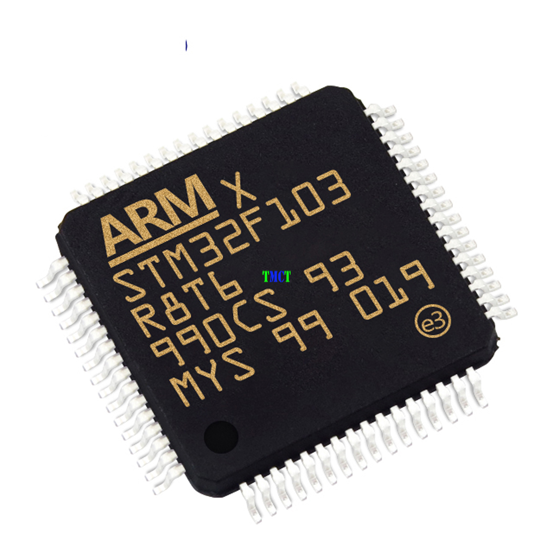
 Reverse Engineering STM32F103R8 Microcomputer Flash Program
Reverse Engineering STM32F103R8 Microcomputer Flash Program can help engineer to extract embedded firmware heximal file from secured mcu stm32f103r8 then clone arm microcontroller stm32f103r8 binary data to new Microprocessor;
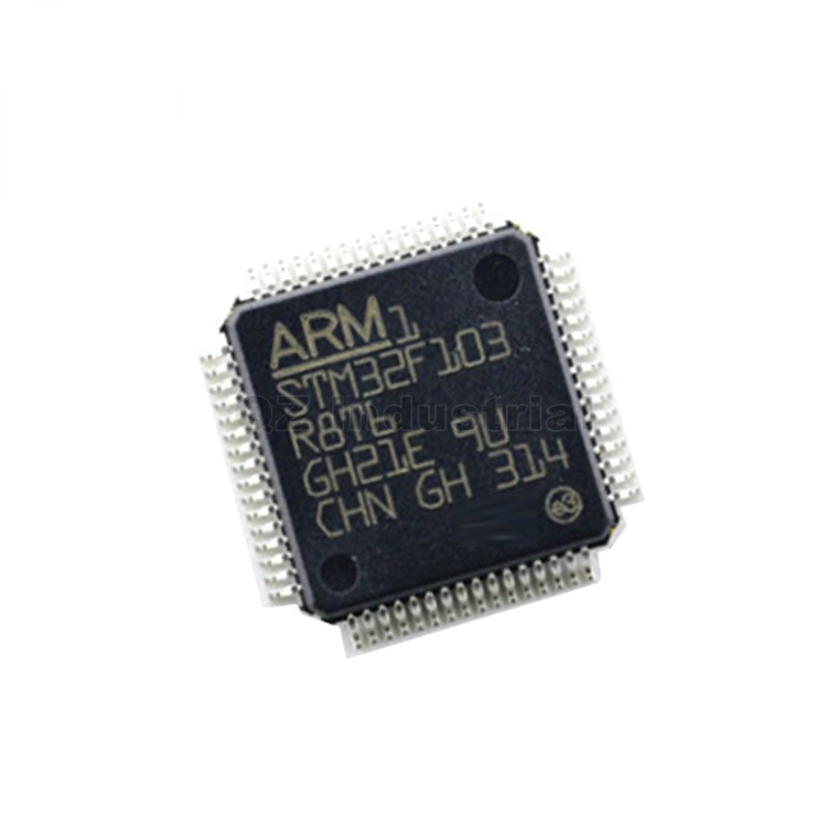
Reverse Engineering STM32F103R8 Microcomputer Flash Program can help engineer to extract embedded firmware heximal file from secured mcu stm32f103r8 then clone arm microcontroller stm32f103r8 binary data to new Microprocessor
System clock selection is performed on startup, however the internal RC 8 MHz oscillator is selected as default CPU clock on reset. An external 4-16 MHz clock can be selected, in which case it is monitored for failure. If failure is detected, the system automatically switches back to the internal RC oscillator when restoring stm32f103c4 arm microcontroller flash binary file. A software interrupt is generated if enabled. Similarly, full interrupt management of the PLL clock entry is available when necessary (for example on failure of an indirectly used external crystal, resonator or oscillator).
Several prescalers allow the configuration of the AHB frequency, the high-speed APB (APB2) and the low-speed APB (APB1) domains. The maximum frequency of the AHB and the high-speed APB domains is 72 MHz. The maximum allowed frequency of the low-speed APB domain is 36 MHz. See Figure 2 for details on the clock tree.
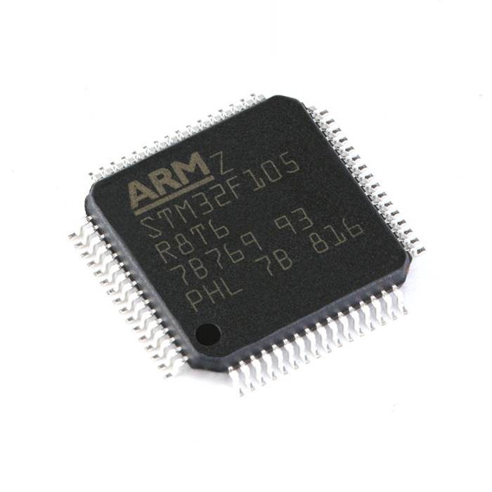
unlock secured STM32F105R8T6 microcontroller fuse bit and extract heximal program file from STM32F105R8T6 microprocessor flash memory
At startup, boot pins are used to select one of three boot options:
- Boot from user Flash
- Boot from System memory
- Boot from embedded SRAM
The boot loader is located in System memory. It is used to reprogram the Flash memory by using USART1. For further details refer to AN2606, available on www.st.com.
- VDD = 2.0 to 3.6 V: external power supply for I/Os and the internal regulator. Provided externally through VDD
- VSSA, VDDA = 2.0 to 3.6 V: external analog power supplies for ADC, reset blocks, RCs and PLL (minimum voltage to be applied to VDDA is 2.4 V when the ADC is used) by restoring stm32f103c8 microcontroller flash program code. VDDA and VSSA must be connected to VDD and VSS,
- VBAT = 8 to 3.6 V: power supply for RTC, external clock 32 kHz oscillator and backup registers (through power switch) when VDD is not present.
For more details on how to connect power pins, refer to Figure 14: Power supply scheme.
El programa flash de microcomputadora STM32F103R8 de ingeniería inversa puede ayudar al ingeniero a extraer el archivo heximal del firmware integrado de mcu stm32f103r8 seguro y luego clonar los datos binarios del microcontrolador stm32f103r8 del brazo al nuevo microprocesador