Archive for the ‘Recover MCU’ Category
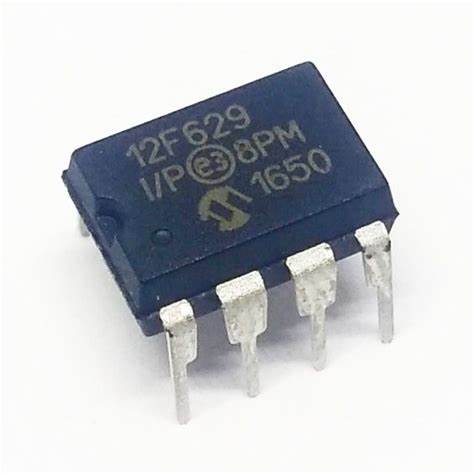
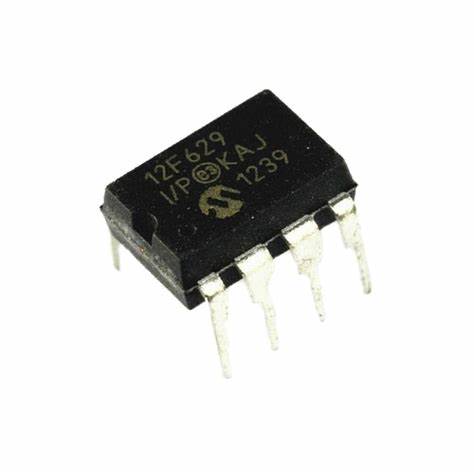
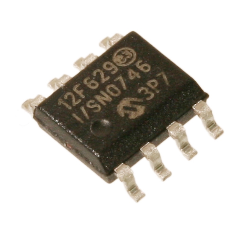
 Recover Locked Microcontroller PIC12F629 Flash Data
Recover Locked Microcontroller PIC12F629 Flash Data needs to attack secured MCU PI12F629 protection system and then read out heximal archive file from original microprocessor PIC12F629;
Recuperar microcontrolador bloqueado PIC12F629 Flash Los datos deben descifrar el bit de fusible de seguridad de MCU asegurado PIC12F629 y luego leer el heximal incrustado de la microcomputadora bloqueada PIC12F629
The primary clock source may never become ready during start-up. In this case, operation is clocked by the INTOSC multiplexer. The OSCCON register will remain in its Reset state until a power managed mode is entered.
para recuperar los datos flash del microcontrolador bloqueado PIC12F629 es necesario atacar el sistema de protección del MCU PI12F629 y luego leer el archivo heximal del microprocesador original PIC12F629;
Entering a power managed mode by loading the OSCCON register and executing a SLEEP instruction will clear the Fail-Safe condition to clone microchip pic12f510 microcontroller flash program. When the Fail-Safe condition is cleared, the clock monitor will resume monitoring the peripheral clock.
Kilitli Mikrodenetleyiciyi Kurtar PIC12F629 Flash Verilerinin güvenli MCU PI12F629 koruma sistemine saldırması ve ardından orijinal mikroişlemci PIC12F629’dan onaltılık arşiv dosyasını okuması gerekir
As previously mentioned, entering a power managed mode clears the Fail-Safe condition. By entering a power managed mode, the clock multiplexer selects the clock source selected by the OSCCON register to read microcontroller pic12f509 flash heximal. Fail-Safe monitoring of the power managed clock source resumes in the power managed mode.
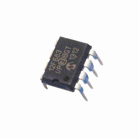
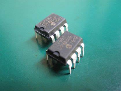
Secured PIC12F683 Microprocessor Heximal Code Recovery
Secured PIC12F683 Microprocessor Heximal Code Recovery is a process to break pic12f683 mcu security fuse bit then read the embedded firmware out from microcontroller pic12f683;
Secured PIC12F683 Microprocessor Heximal Code Recovery è un processo per rompere il bit del fusibile di sicurezza mcu pic12f683, quindi leggere il firmware incorporato dal microcontrollore pic12f683
Clock failure is tested for on the falling edge of the sample clock. If a sample clock falling edge occurs while CM is still set, a clock failure has been detected. This causes the following:
- the FSCM generates an oscillator fail interrupt by setting bit, OSCFIF (PIR2<7>);
- the system clock source is switched to the internal oscillator block (OSCCON is not updated to show the current clock source – this is the Fail-Safe condition); and
- the WDT is
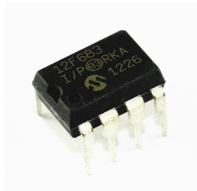
asegurado PIC12F683 microprocesador de recuperación de código heximal es un proceso para romper pic12f683 mcu fusible de seguridad de bits a continuación, leer el firmware embebido a cabo desde el microcontrolador pic12f683;
Since the postscaler frequency from the internal oscil- lator block may not be sufficiently stable, it may be desirable to select another clock configuration and enter an alternate power managed mode when breaking PIC18F242 MCU flash memory (see Section 19.3.1 “Special Considerations for Using Two-Speed Start-up” and Section 3.1.3 “Multiple Sleep Commands” for more details). This can be done to attempt a partial recovery, or execute a controlled shutdown.
Güvenli PIC12F683 Mikroişlemci Onaltılı Kod Kurtarma, pic12f683 mcu güvenlik sigorta bitini kırmak ve ardından gömülü bellenimi mikrodenetleyiciden okumak için bir süreçtir pic12f683
To use a higher clock speed on wake-up, the INTOSC or postscaler clock sources can be selected to provide a higher clock speed by setting bits, IFRC2:IFRC0 when PIC18F252 microcontroller flash memory program recovery, immediately after Reset. For wake-ups from Sleep, the INTOSC or postscaler clock sources can be selected by setting IFRC2:IFRC0 prior to entering Sleep mode.
Restoring Locked PIC12F635 Microprocessor Flash Code
Restoring Locked PIC12F635 Microprocessor Flash Code is a process to read embedded program out from PIC12F635 secured MCU and then copy firmware to new microcontroller PIC12F635;
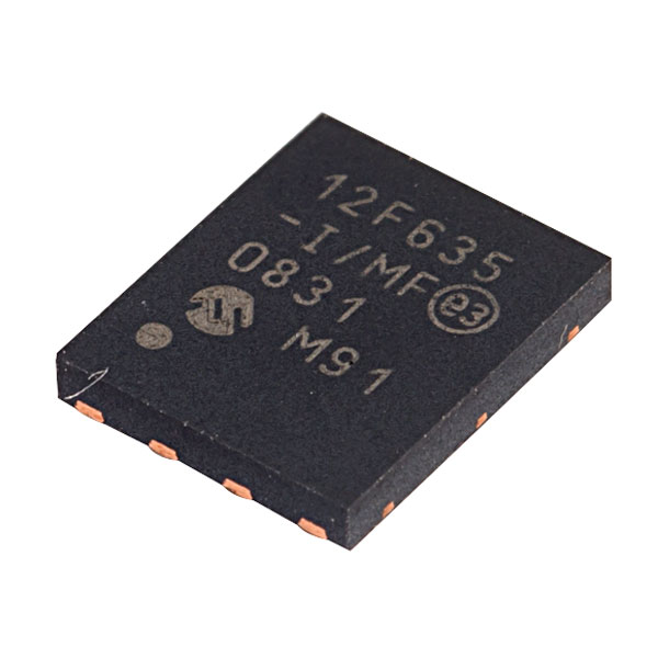
La restauration du code flash du microprocesseur PIC12F635 verrouillé est un processus permettant de lire le programme intégré à partir du MCU sécurisé PIC12F635, puis de copier le micrologiciel sur le nouveau microcontrôleur PIC12F635
The Two-Speed Start-up feature helps to minimize the latency period from oscillator start-up to code execution by allowing the microcontroller to use the INTRC oscillator as a clock source until the primary clock source is available. It is enabled by setting the IESO bit in Configuration Register 1H (CONFIG1H<7>).
Two-Speed Start-up is available only if the primary oscil- lator mode is LP, XT, HS or HSPLL (crystal-based modes). Other sources do not require an OST start-up delay to read microcontroller pic12f509 flash heximal; for these, Two-Speed Start-up is disabled.
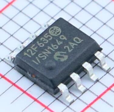
Восстановление заблокированного кода флэш-памяти микропроцессора PIC12F635 — это процесс считывания встроенной программы из защищенного микроконтроллера PIC12F635 с последующим копированием прошивки на новый микроконтроллер PIC12F635.
When enabled, Resets and wake-ups from Sleep mode cause the device to configure itself to run from the internal oscillator block as the clock source, following the time-out of the Power-up Timer after a Power-on Reset is enabled. This allows almost immediate code execution while the primary oscillator starts and the OST is running to clone microchip pic12f510 microcontroller flash program. Once the OST times out, the device automatically switches to PRI_RUN mode.
Locked Microchip PIC12F615 Processor Data Restoration
Locked Microchip PIC12F615 Processor Data Restoration is a process to copy embedded firmware from original MCU PIC12F615 flash memory after break off the tamper resistance system of PIC12F615 locked microcontroller;
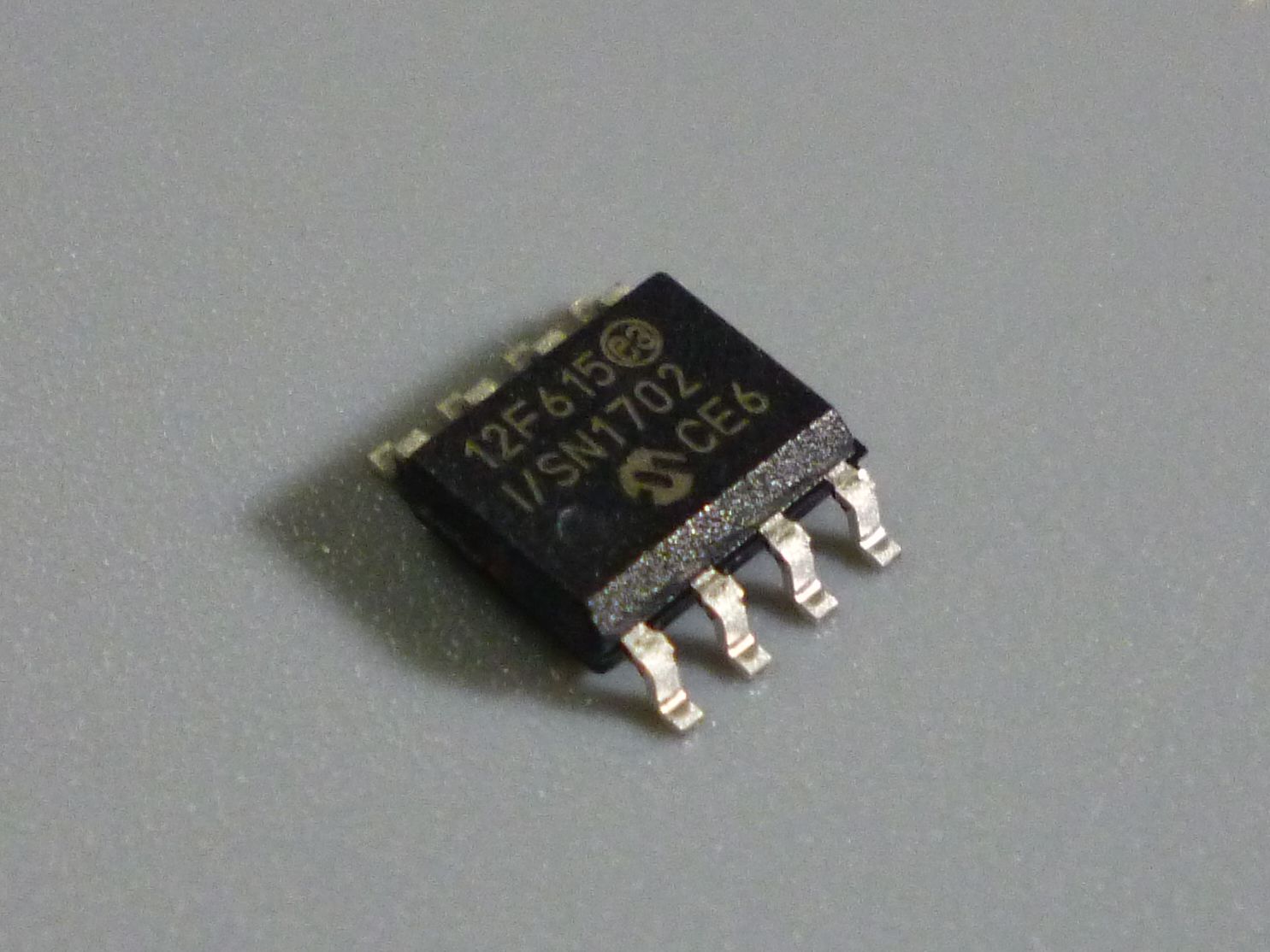
A Restauração de Dados do Processador PIC12F615 de Microchip Bloqueado é um processo para copiar o firmware incorporado da memória flash MCU PIC12F615 original após interromper o sistema de resistência à violação do microcontrolador bloqueado PIC12F615;
The Configuration bits can be programmed (read as ‘0’), or left unprogrammed (read as ‘1’), to select vari- ous device configurations. These bits are mapped starting at program memory location 300000h.
The user will note that address 300000h is beyond the user program memory space. In fact, it belongs to the configuration memory space (300000h-3FFFFFh), which can only be accessed using table reads and table writes.
Programming the Configuration registers is done in a manner similar to programming the Flash memory. The EECON1 register WR bit starts a self-timed write to the Configuration register. In normal operation mode, a TBLWT instruction, with the TBLPTR pointing to the Configuration register, sets up the address and the data for the Configuration register write.
Il ripristino dei dati del processore PIC12F615 del microchip bloccato è un processo per copiare il firmware incorporato dalla memoria flash originale dell’MCU PIC12F615 dopo aver interrotto il sistema di resistenza alle manomissioni del microcontrollore bloccato PIC12F615;
Setting the WR bit starts a long write to the Configuration register. The Configuration registers are written a byte at a time. To write or erase a configuration cell by breaking pic12f635 locked microprocessor fuse bit, a TBLWT instruction can write a ‘1’ or a ‘0’ into the cell. For additional details on Flash programming, refer to Section 6.5 “Writing to Flash Program Memory”.
bit 7 IESO: Internal External Switchover bit
1 = Internal External Switchover mode enabled
0 = Internal External Switchover mode disabled bit 6 FSCM: Fail-Safe Clock Monitor Enable bit
1 = Fail-Safe Clock Monitor enabled
0 = Fail-Safe Clock Monitor disabled
bit 5-4 Unimplemented: Read as ‘0’
bit 3-0 FOSC<3:0>: Oscillator Selection bits
11xx = External RC oscillator, CLKO function on RA6
1001 = Internal RC oscillator, CLKO function on RA6 and port function on RA7 1000 = Internal RC oscillator, port function on RA6 and port function on RA7 0111 = External RC oscillator, port function on RA6 when breaking pic12f609 locked mcu flash memory;
0110 = HS oscillator, PLL enabled (clock frequency = 4 x FOSC1)
0101 = EC oscillator, port function on RA6 0100 = EC oscillator, CLKO function on RA6 0010 = HS oscillator
0001 = XT oscillator
0000 = LP oscillator
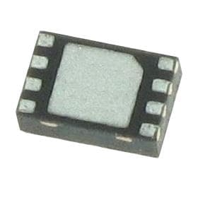
Recover PIC12F612 Secured Microchip MCU Flash Heximal
recover PIC12F612 Secured Microchip MCU flash heximal after attack PIC12F612 locked microcontroller security fuse bit, then dump embedded firmware from encrypted microprocessor PIC12F612 from its flash and eeprom memory;
recupere PIC12F612 Secured Microchip MCU flash heximal después del ataque PIC12F612 bloqueó el bit de fusible de seguridad del microcontrolador, luego descargue el firmware integrado del microprocesador cifrado PIC12F612 de su memoria flash y eeprom;
A complete discussion of device Resets and interrupts is available in previous sections of this data sheet.
In addition to their Power-up and Oscillator Start-up Timers provided for Resets, PIC12F612 devices have a Watchdog Timer, which is either permanently enabled via the Configuration bits, or software controlled (if configured as disabled) when break pic12f629 microcontroller flash memory.
The inclusion of an internal RC oscillator also provides the additional benefits of a Fail-Safe Clock Monitor (FSCM) and Two-Speed Start-up. FSCM provides for background monitoring of the peripheral clock and automatic switchover in the event of its failure.
recuperați PIC12F612 Secured Microcip MCU flash heximal după atac PIC12F612 blocat bitul siguranței de securitate al microcontrolerului, apoi descărcați firmware-ul încorporat de la microprocesorul criptat PIC12F612 din memoria flash și eeprom;
Two- Speed Start-up enables code to be executed almost immediately on start-up, while the primary clock source completes its start-up delays to copy pic12f675 secured microcontroller flash memory. All of these features are enabled and configured by setting the appropriate Configuration register bits.
Replicate PIC12F519 Microprocessor Flash Program
Replicate PIC12F519 Microprocessor Flash Program can help engineer to unlock ic chip secured pic12f519 binary from its flash memory, to readout microchip locked pic12f519 source code;
Çoğaltma PIC12F519 Mikroişlemci Flash Programı, mühendisin ic çip korumalı pic12f519 ikili dosyasını flash belleğinden açmasına, mikroçip kilitli pic12f519 kaynak kodunu okumasına yardımcı olabilir
The LVD module has an additional feature that allows the user to supply the trip voltage to the module from an external source. This mode is enabled when bits, LVDL3:LVDL0, are set to ‘1111’. In this state, the com- parator input is multiplexed from the external input pin when breaking microcontroller pic12f629 flash, LVDIN (Figure 18-3). This gives users flexibility, because it allows them to configure the Low-Voltage Detect interrupt to occur at any voltage in the valid operating range.
Kilitli mikrodenetleyici PIC12F519’un kurcalamaya karşı direnç sistemini kırma ve PIC12F519 MCU flash bellekten onaltılık dosyayı kurtarma;
bit 7-6 Unimplemented: Read as ‘0’
bit 5 IRVST: Internal Reference Voltage Stable Flag bit
1 = Indicates that the Low-Voltage Detect logic will generate the interrupt flag at the specified voltage range
0 = Indicates that the Low-Voltage Detect logic will not generate the interrupt flag at the specified volt- age range and the LVD interrupt should not be enabled by breaking dspic30f4011 mcu flash memory;
bit 4 LVDEN: Low-Voltage Detect Power Enable bit
1 = Enables LVD, powers up LVD circuit
0 = Disables LVD, powers down LVD circuit
bit 3-0 LVDL<3:0>: Low-Voltage Detection Limit bits(1)
1111 = External analog input is used (input comes from the LVDIN pin)
1110 = 4.04V-5.15V
1101 = 3.76V-4.79V
1100 = 3.58V-4.56V
1011 = 3.41V-4.34V
1010 = 3.23V-4.11V
1001 = 3.14V-4.00V
1000 = 2.96V-3.77V
0111 = 2.70V-3.43V
0110 = 2.53V-3.21V
0101 = 2.43V-3.10V
0100 = 2.25V-2.86V
0011 = 2.16V-2.75V
0010 = 1.99V-2.53V
0001 = Reserved
0000 = Reserved
Note 1: LVDL<3:0> modes, which result in a trip point below the valid operating voltage of the device, are not tested.
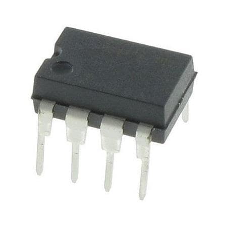
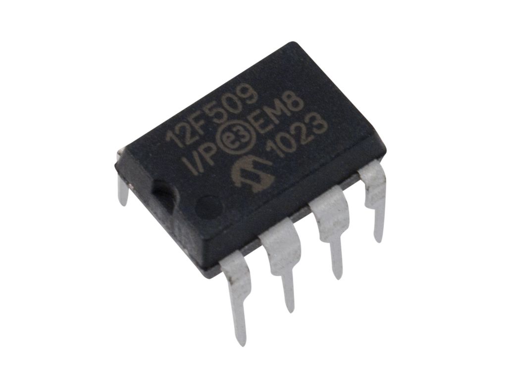
Read Microcontroller PIC12F509 Flash Heximal
Read Microcontroller PIC12F509 Flash Heximal needs to crack pic mcu pic12f509 security fuse bit, extract mcu pic12f509 embedded firmware from its flash memory;
Leggi il microcontrollore PIC12F509 Flash Heximal ha bisogno di rompere il bit del fusibile di sicurezza pic mcu pic12f509, estrarre il firmware incorporato mcu pic12f509 dalla sua memoria flash;
Figure 17-3 shows the operation of the A/D converter after the GO bit has been set and the ACQT2:ACQT0 bits are cleared. A conversion is started after the following instruction to allow entry into Low-Power Sleep mode before the conversion begins.
Figure 17-4 shows the operation of the A/D converter after the GO bit has been set and the ACQT2:ACQT0 bits are set to ‘010’ and selecting a 4 TAD acquisition time before the conversion starts.
Clearing the GO/DONE bit during a conversion will abort the current conversion. The A/D Result register pair will NOT be updated with the partially completed A/ D conversion sample when break off pic12f509 eeprom and flash memory fuse bit. This means the ADRESH:ADRESL registers will continue to contain the value of the last completed conversion (or the last value written to the ADRESH:ADRESL registers).
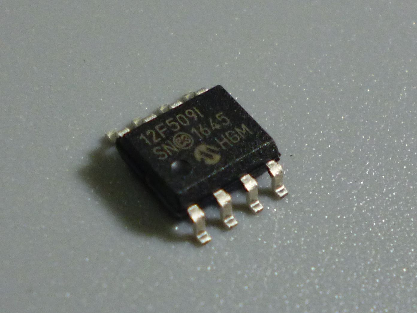
Copia il programma di memoria flash del processore PIC12F509 del microchip e riscrivi il file esadecimale o binario sul nuovo microcontrollore PIC12F509 per la clonazione dell’MCU
After the A/D conversion is completed or aborted, a 2 TAD wait is required before the next acquisition can be started. After this wait, acquisition on the selected channel is automatically started.
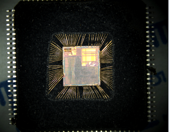
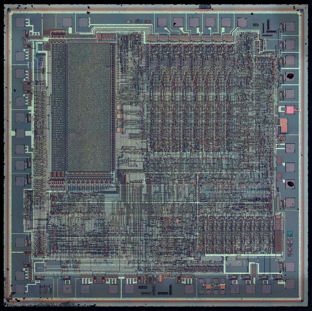
Microcontroller STM32F091VC Flash Heximal Recovery
Microcontroller STM32F091VC Flash Heximal Recovery needs to crack arm stm32f091vc microprocessor security fuse bit, duplicate flash firmware from arm mcu stm32f091vc;
Unless otherwise specified, the minimum and maximum values are guaranteed in the worst conditions of ambient temperature, supply voltage and frequencies by tests in production on 100% of the devices with an ambient temperature at TA = 25 °C and TA = TAmax (given by the selected temperature range).
Data based on characterization results, design simulation and/or technology characteristics are indicated in the table footnotes and are not tested in production to break stm32f301k6 encrypted microprocessor flash memory. Based on characterization, the minimum and maximum values refer to sample tests and represent the mean value plus or minus three times the standard deviation (mean±3s).
microcontrolador STM32F091VC flash heximal recuperación necesita para descifrar brazo stm32f091vc microprocesador seguridad fusible bit, duplicar flash firmware de brazo mcu stm32f091vc;
Unless otherwise specified, typical data are based on TA = 25 °C, VDD = VDDA = 3.3 V. They are given only as design guidelines and are not tested. Typical ADC accuracy values are determined by characterization of a batch of samples from a standard diffusion lot over the full temperature range when restoring secured stm32f301r8 mcu flash firmware, where 95% of the devices have an error less than or equal to the value indicated (mean±2s).
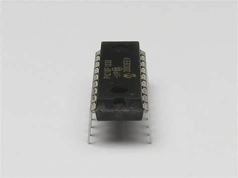
Clone Microchip PIC16LF84 Controller Firmware
Clone Microchip PIC16LF84 Controller Firmware from its locked processor’s flash and eeprom memory, and decode embedded firmware from secured MCU pic16lf84;
Using the internal oscillator as the clock source can eliminate the need for up to two external oscillator pins, which can then be used for digital I/O. Two distinct configurations are available:
- In INTIO1 mode, the OSC2 pin outputs FOSC/4, while OSC1 functions as RA7 for digital input and output.
- In INTIO2 mode, OSC1 functions as RA7 and OSC2 functions as RA6, both for digital input and output.
The internal oscillator block is calibrated at the factory to produce an INTOSC output frequency of 8.0 MHz to restore pic18f1220t processor embedded program. This changes the frequency of the INTRC source from its nominal 31.25 kHz.
Peripherals and features that depend on the INTRC source will be affected by this shift in frequency. Once set during factory calibration when decrypting pic18f1230 microcontroller flash memory, the INTRC frequency will remain within ±2% as temperature and VDD change across their full specified operating ranges.
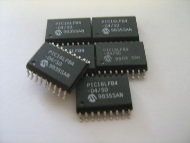
clonar el firmware del controlador PIC16LF84 del microchip de la memoria flash y eeprom de su procesador bloqueado, y decodificar el firmware integrado del MCU pic16lf84 seguro
The internal oscillator’s output has been calibrated at the factory, but can be adjusted in the user’s applica- tion. This is done by writing to the OSCTUNE register. The tuning sensitivity is constant throughout the tuning range.
Microprocessor PIC18F1330 Flash Data Recovery
Microprocessor PIC18F1330 Flash Data Recovery needs to unlock encrypted microchip pic18f1330 mcu security fuse bit, and extract locked microchip pic18f1330 mcu heximal file;
The EC and ECIO Oscillator modes require an external clock source to be connected to the OSC1 pin. There is no oscillator start-up time required after a Power-on Reset, or after an exit from Sleep mode.
In the EC Oscillator mode, the oscillator frequency divided by 4 is available on the OSC2 pin. This signal may be used for test purposes, or to synchronize other logic.
The ECIO Oscillator mode functions like the EC mode, except that the OSC2 pin becomes an additional gen- eral purpose I/O pin. The I/O pin becomes bit 6 of PORTA (RA6).
For timing insensitive applications, the “RC” and “RCIO” device options offer additional cost savings . The RC oscillator frequency is a function of the supply voltage when recover pic18f1330 microcontroller code, the resistor (REXT) and capacitor (CEXT) values and the operating temperature.
microprocessador PIC18F1330 recuperação de dados flash precisa desbloquear microchip criptografado pic18f1330 mcu bit fusível de segurança, e extrair microchip bloqueado pic18f1330 mcu arquivo heximal
In addition to this, the oscillator frequency will vary from unit to unit due to normal manufacturing variation. Furthermore, the difference in lead frame capacitance between package types will also affect the oscillation frequency, espe- cially for low CEXT values by . The user also needs to take into account variation, due to tolerance of external R and C components used by breaking microcontroller pic18f14k22 flash memory.