 Clone Microchip PIC12F510 Microcontroller Flash Program
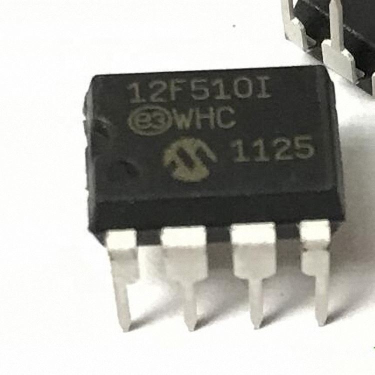
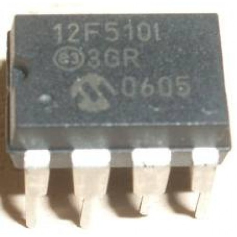
Clone Microchip PIC12F510 Microcontroller Flash Program and rewrite the heximal file to new MCU PIC12F510, the lock bit of PIC12F510 microprocessor will be unlocked and original firmware can be copied from pic12f510 MCU;
Klonuokite mikroschemą PIC12F510 mikrovaldiklio Flash programa ir perrašykite šešioliktainį failą į naują MCU PIC12F510, PIC12F510 mikroprocesoriaus blokavimo bitas bus atrakintas ir originali programinė įranga gali būti nukopijuota iš pic12f510 MCU.
An A/D conversion can be started by the “special event trigger” of the CCP1 module. This requires that the CCP1M3:CCP1M0 bits (CCP1CON<3:0>) be programmed as ‘1011’ and that the A/D module is enabled (ADON bit is set). When the trigger occurs, the GO/ DONE bit will be set, starting the A/D acquisition and conversion and the Timer1 (or Timer3) counter will be reset to zero.
Timer1 (or Timer3) is reset to auto-matically repeat the A/D acquisition period with minimal software overhead (moving ADRESH/ADRESL to the desired location). The appropriate analog input channel must be selected and the minimum acquisition period is either timed by the user to unlock pic12f510 mcu fuse bit, or an appropriate TACQ time selected before the “special event trigger” sets the GO/DONE bit (starts a conversion).
Klon Mikrochip PIC12F510 Mikrokontroller Flash Programm a schreift d’heximal Datei op den neie MCU PIC12F510, de Sperrbit vum PIC12F510 Mikroprozessor gëtt opgehuewen an d’originell Firmware kann vum pic12f510 MCU kopéiert ginn
If the A/D module is not enabled (ADON is cleared), the “special event trigger” will be ignored by the A/D module, but will still reset the Timer1 (or Timer3) counter.
x = unknown, u = unchanged, q = depends on CONFIG1H<3:0>, – = unimplemented, read as ‘0’.
Shaded cells are not used for A/D conversion.
Note 1: RA5 port bit is available only as an input pin when the MCLRE bit in the Configuration register is ‘0’.
2: RA6 and TRISA6 are available only when the primary oscillator mode selection offers RA6 as a port pin; otherwise, RA6 always reads ‘0’, TRISA6 always reads ‘1’ and writes to both are ignored (see CONFIG1H<3:0>).
3: RA7 and TRISA7 are available only when the internal RC oscillator is configured as the primary oscillator in CON- FIG1H<3:0> by cracking microcontroller pic12f510 flash memory program; otherwise, RA7 always reads ‘0’, TRISA7 always reads ‘1’ and writes to both are ignored.