Archive for the ‘Recover Chip’ Category
 Recover MCU PIC12C509 Program
Recover MCU PIC12C509 Program is a process to readout heximal file from embedded microcontroller pic12c509 after crack mcu fuse bit;
The high performance of the PIC12C5XX family can be attributed to a number of architectural features commonly found in RISC microprocessors. To begin with, the PIC12C5XX uses a Harvard architecture in which program and data are accessed on separate buses.
This improves bandwidth over traditional von Neumann architecture where program and data are fetched on the same bus. Separating program and data memory further allows instructions to be sized differently than the 8-bit wide data word. Instruction opcodes are 12-bits wide making it possible to have all single word instructions if break microcontroller pic16c716 hex.
A 12-bit wide program memory access bus fetches a 12-bit instruction in a single cycle. A two-stage pipeline overlaps fetch and execution of instructions. Consequently, all instructions (33) execute in a single cycle (1µs @ 4MHz) except for program branches.
The table below lists program memory (EPROM), data memory (RAM), ROM memory, and non-volatile (EEPROM) for each device. The PIC12C5XX device contains an 8-bit ALU and working register. The ALU is a general purpose arithmetic unit. It performs arithmetic and Boolean functions between data in the working register and any register file after attack pic16cr84 MCU memory
The ALU is 8-bits wide and capable of addition, subtraction, shift and logical operations. Unless otherwise mentioned, arithmetic operations are two’s complement in nature. In two-operand instructions, typically one operand is the W (working) register. The other operand is either a file register or an immediate constant. In single operand instructions, the operand is either the W register or a file register.
The register is an 8-bit working register used for ALU operations. It is not an addressable register. Depending on the instruction executed, the ALU may affect the values of the Carry (C), Digit Carry (DC), and Zero (Z) bits in the STATUS register.
Th e C and DC bits operate as a borrow and digit borrow out bit, respectively, in subtraction. See theSUBWF andADDWF instructions for examples. A simplified block diagram is shown in Figure 3-1, with the corresponding device pins described in Table 3-1. The PIC12C5XX can directly or indirectly address its register files and data memory.
All special function registers including the program counter are mapped in the data memory. The PIC12C5XX has a highly orthogonal (symmetrical) instruction set that makes it possible to carry out any operation on any register using any addressing mode. This symmetrical nature and lack of ‘special optimal situations’ make programming with the PIC12C5XX simple yet efficient. In addition, the learning curve is reduced significantly.
Recovery Microcontroller ATmega861P Heximal
Recovery Microcontroller ATmega861P Heximal needs to unlock protected mcu atmega861p memory and then readout the embedded code from atmega861p processor flash memory;
The OCR2x Register is double buffered when using any of the Pulse Width Modulation (PWM) modes. For the Normal and Clear Timer on Compare (CTC) modes of operation, the double buffering is disabled.
The double buffering synchronizes the update of the OCR2x Compare Register to either top or bottom of the counting sequence. The synchronization prevents the occurrence of odd-length, non-symmetrical PWM pulses, thereby making the output glitch-free before attack cpld xc9536xl memory.
The OCR2x Register access may seem complex, but this is not case. When the double buffering is enabled, the CPU has access to the OCR2x Buffer Register, and if double buffering is disabled the CPU will access the OCR2x directly.
In non-PWM waveform generation modes, the match output of the comparator can be forced by writing a one to the Force Output Compare (FOC2x) bit.
Forcing compare match will not set the OCF2x Flag or reload/clear the timer, but the OC2x pin will be updated as if a real compare match had occurred (the COM2x1:0 bits settings define whether the OC2x pin is set, cleared or toggled) when attack pic16c558 Microcontroller.
All CPU write operations to the TCNT2 Register will block any compare match that occurs in the next timer clock cycle, even when the timer is stopped. This feature allows OCR2x to be initialized to the same value as TCNT2 without triggering an interrupt when the Timer/Counter clock is enabled.
Since writing TCNT2 in any mode of operation will block all compare matches for one timer clock cycle, there are risks involved when changing TCNT2 when using the Output Compare channel, independently of whether the Timer/Counter is running or not.
If the value written to TCNT2 equals the OCR2x value, the compare match will be missed, resulting in incorrect waveform generation. Similarly, do not write the TCNT2 value equal to BOTTOM when the counter is downcounting.
The setup of the OC2x should be performed before setting the Data Direction Register for the port pin to output. The easiest way of setting the OC2x value is to use the Force Output Compare (FOC2x) strobe bit in Normal mode.
The OC2x Register keeps its value even when changing between Waveform Generation modes. Be aware that the COM2x1:0 bits are not double buffered together with the compare value. Changing the COM2x1:0 bits will take effect immediately.
Recover Chip PIC12C508 Software
Recover Chip PIC12C508 Software needs to firstly extract locked code from mcu pic12c508 mcu and then copy the embedded heximal to new microcontroller pic12c508;
High-Performance RISC CPU:
· Only 33 single word instructions to learn
· All instructions are single cycle (1 µs) except for program branches which are two-cycle
· Operating speed: DC – 4 MHz clock input DC – 1 µs instruction cyc
12-bit wide instructions
8-bit wide data path
Seven special function hardware registers
Two-level deep hardware stack
Direct, indirect and relative addressing modes for data and instructions
· Internal 4 MHz RC oscillator with programmable calibration
· In-circuit serial programming
· 8-bit real time clock/counter (TMR0) with 8-bit programmable prescaler
· Power-On Reset (POR)
· Device Reset Timer (DRT)
· Watchdog Timer (WDT) with its own on-chip RC oscillator for reliable operation
· Programmable code-protection
· 1,000,000 erase/write cycle EEPROM data memory
· EEPROM data retention > 40 years
· Power saving SLEEP mode
· Wake-up from SLEEP on pin change
· Internal weak pull-ups on I/O pins
· Internal pull-up on MCLR pin
· Selectable oscillator options:
– INTRC: Internal 4 MHz RC oscillator
– EXTRC: External low-cost RC oscillator
– XT: Standard crystal/resonator
– LP: Power saving, low frequency crystal
CMOS Technology:
· Low power, high speed CMOS EPROM/ROM technology
· Fully static design
· Wide operating voltage range
· Wide temperature range:
– Commercial: 0°C to +70°C
– Industrial: -40°C to +85°C
– Extended: -40°C to +125°C
· Low power consumption
– < 2 mA @ 5V, 4 MHz
Circuit Engineering Company Limited continues to be recognized as the Southern China Leader in Services for IC Read, MCU Crack, Chip Extract, Microcontroller Recover service.
With the advancement of today’s modern circuit board technology, it is more important than ever to have specialists available to help you at a moment’s notice. Our engineering and commercial teams collectively have a vast amount of electronic experience covering field include Consumer Electronics, Industrial Automation Electronics, Wireless Communication Electronics., etc. For more information please contact us through email.
Recover MCU PIC16C558 Program
We can Recover MCU PIC16C558 Program, please view the MCU PIC16C558 features for your reference:
The UV erasable version, offered in CERDIP package is optimal for prototype development and pilot programs. This version can be erased and reprogrammed to any of the oscillator modes if Recover MCU.
Microchip’s PICSTART® and PROMATE® programmers both support programming of the PIC16C558
Microchip offers a QTP Programming Service for factory production orders. This service is made available for users who choose not to program a medium to high quantity of units and whose code patterns have stabilized when Recover MCU. The devices are identical to the OTP devices but with all EPROM locations and configuration options already programmed by the factory. Certain code and prototype verification procedures apply before production shipments are available after Recover MCU.
Microchip offers a unique programming service where a few user-defined locations in each device are programmed with different serial numbers. The serial numbers may be random, pseudo-random or sequential before Recover MCU.
The high performance of the PIC16C55X(A) family can be attributed to a number of architectural features commonly found in RISC microprocessors. To begin with, the PIC16C55X(A) uses a Harvard architecture, in which, program and data are accessed from separate memories using separate busses after Recover MCU. This improves bandwidth over traditional von Neumann architecture where program and data are fetched from the same memory. Separating program and data memory further allows instructions to be sized differently than 8-bit wide data words. Instruction opcodes are 14-bits wide making it possible to have all single word instructions when Recover MCU.
A 14-bit wide program memory access bus fetches a 14-bit instruction in a single cycle. A two-stage pipeline overlaps fetch and execution of instructions. Consequently, all instructions (35) execute in a single-cycle (200 ns @ 20 MHz) except for program branches if Recover MCU.
The PIC16C554(A) addresses 512 x 14 on-chip program memory. The PIC16C556A addresses 1K x 14 program memory. The PIC16C558(A) addresses 2K x 14 program memory. All program memory is internal. The PIC16C55X(A) can directly or indirectly address its register files or data memory before Recover MCU. All special function registers including the program counter are mapped into the data memory. The PIC16C55X(A) have an orthogonal (symmetrical) instruction set that makes it possible to carry out any operation on any register using any addressing mode after Recover MCU. This symmetrical nature and lack of ‘special optimal situations’ make programming with the PIC16C55X(A) simple yet efficient. In addition, the learning curve is reduced significantly.
The availability of OTP devices is especially useful for customers who need the flexibility for frequent code updates and small volume applications. In addition to the program memory, the configuration bits must also be programmed after Recover MCU.
Recovery Chip ATMEGA2560PV Program
We can Recovery CHIP ATMEGA2560PV Program, please view the CHIP ATMEGA2560PV features for your reference:
In this example, Timer/Counter2 provides the carrier, while the modulating signal is generated by the Output Compare unit C of the Timer/Counter1 when Recovery CHIP program.
The resolution of the PWM signal (OC1C) is reduced by the modulation. The reduction factor is equal to the number of system clock cycles of one period of the carrier (OC0A).
In this example the resolution is reduced by a factor of two. The reason for the reduction is illustrated in Figure 66 at the second and third period of the PB7 output when PORTB7 equals zero if Recovery CHIP program.
The period 2 high time is one cycle longer than the period 3 high time, but the result on the PB7 output is equal in both periods. Timer/Counter2 is a general purpose, single channel, 8-bit Timer/Counter module. The main features are before Recovery CHIP program:
Single Channel Counter
Clear Timer on Compare Match (Auto Reload)
Glitch-free, Phase Correct Pulse Width Modulator (PWM) after Recovery CHIP program
Frequency Generator
10-bit Clock Prescaler
Overflow and Compare Match Interrupt Sources (TOV2, OCF2A and OCF2B)
Allows Clocking from External 32 kHz Watch Crystal Independent of the I/O Clock
A simplified block diagram of the 8-bit Timer/Counter is shown in Figure 60.. For the actual placement of I/O pins, see “Pin Configurations” on page 2. CPU accessible I/O Registers, including I/O bits and I/O pins, are shown in bold. The device-specific I/O Register and bit locations are listed in the “8-bit Timer/Counter Register Description” on page 184 if Recovery CHIP program.
The Power Reduction Timer/Counter2 bit, PRTIM2, in “Power Reduction Register 0 – PRR0” on page 54 must be written to zero to enable Timer/Counter2 module before Recovery CHIP program.
The Timer/Counter (TCNT2) and Output Compare Register (OCR2A and OCR2B) are 8-bit registers. Interrupt request (abbreviated to Int.Req.) signals are all visible in the Timer Interrupt Flag Register (TIFR2). All interrupts are individually masked with the Timer Interrupt Mask Register (TIMSK2). TIFR2 and TIMSK2 are not shown in the figure when Recovery CHIP program.
The Timer/Counter can be clocked internally, via the prescaler, or asynchronously clocked from the TOSC1/2 pins, as detailed later in this section. The asynchronous operation is controlled by the Asynchronous Status Register (ASSR). The Clock Select logic block controls which clock source the Timer/Counter uses to increment (or decrement) its value. The Timer/Counter is inactive when no clock source is selected. The output from the Clock Select logic is referred to as the timer clock (clkT2). The double buffered Output Compare Register (OCR2A and OCR2B) are compared with the Timer/Counter value at all times after Recovery CHIP program.
The result of the compare can be used by the Waveform Generator to generate a PWM or variable frequency output on the Output Compare pins (OC2A and OC2B). See “Output Compare Unit” on page 175. for details.
The compare match event will also set the Compare Flag (OCF2A or OCF2B) which can be used to generate an Output Compare interrupt request. Many register and bit references in this document are written in general form. A lower case “n” replaces the Timer/Counter number, in this case 2. However, when using the register or bit defines in a program, the precise form must be used, i.e., TCNT2 for accessing Timer/Counter2 counter value and so on before Recovery CHIP program.
The definitions in Table 84 are also used extensively throughout the section.
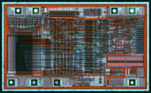
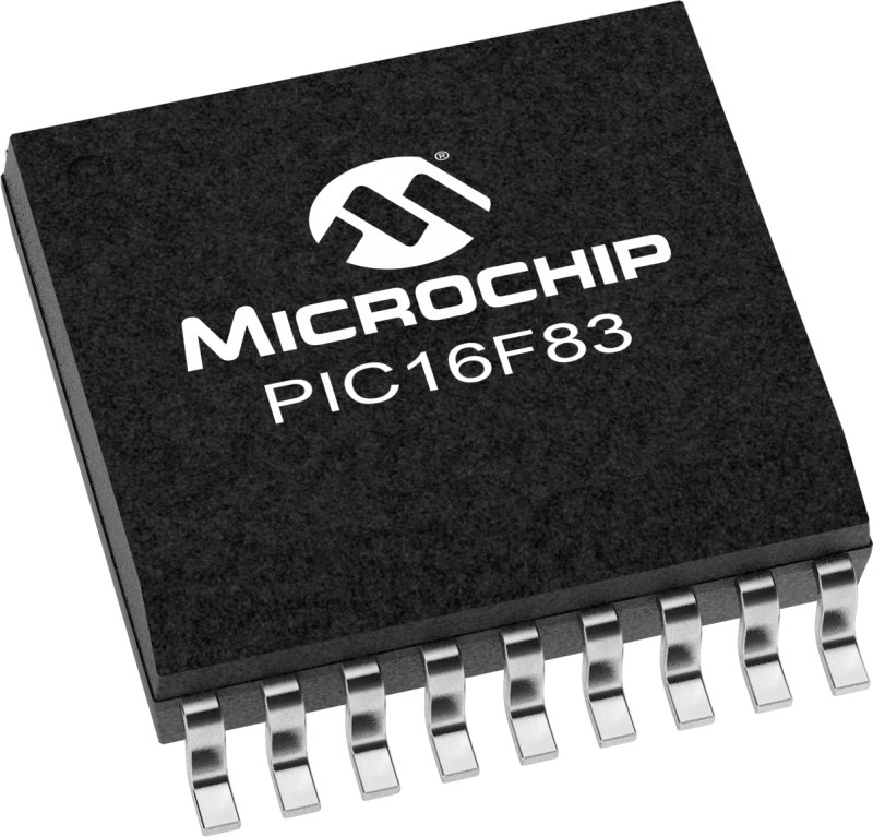
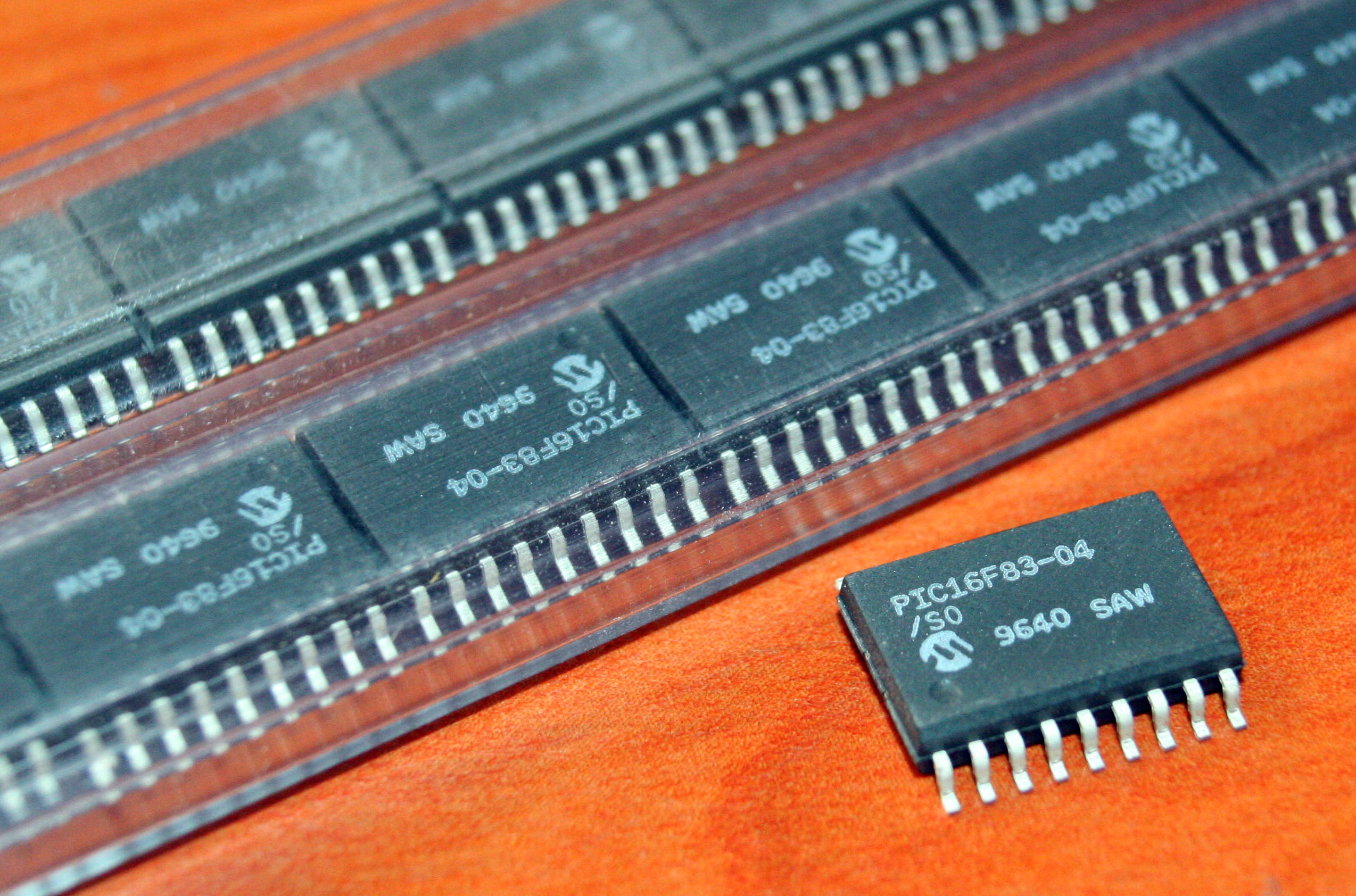
Recover Chip PIC16F83 Eeprom
Recover Chip PIC16F83 Eeprom content by cracking locked microcontroller pic16f83 security fuse bit and then extract embedded code from microchip MCU;
Recover Chip PIC16F83 Eeprom content by cracking locked microcontroller pic16f83 security fuse bit and then extract embedded code from microchip MCU
We can Recover Chip PIC16F83 Eeprom, please view the Chip PIC16F83 features for your reference:
High Performance RISC CPU Features:
• Only 35 single word instructions to learn
• All instructions single cycle except for program branches which are two-cycle Operating speed: DC – 10 MHz clock input
DC – 400 ns instruction cycle
14-bit wide instructions
8-bit wide data path
15 special function hardware registers
Eight-level deep hardware stack
Direct, indirect and relative addressing modes
Four interrupt sources:
– External RB0/INT pin
– TMR0 timer overflow
– PORTB<7:4> interrupt on change
– Data EEPROM write complete
· 1000 erase/write cycles Flash program memory
· 10,000,000 erase/write cycles EEPROM data memory
· EEPROM Data Retention > 40 years
Peripheral Features:
· 13 I/O pins with individual direction control
· High current sink/source for direct LED drive
– 25 mA sink max. per pin before Recover Chip
– 20 mA source max. per pin
· TMR0: 8-bit timer/counter with 8-bit programmable prescaler
Special Microcontroller Features:
· In-Circuit Serial Programming (ICSP™) – via two pins (ROM devices support only Data EEPROM programming)
· Power-on Reset (POR)
crack pic16f83 microchip processor and copy mcu pic16f83 memory file
· Power-up Timer (PWRT)
· Oscillator Start-up Timer (OST)
· Watchdog Timer (WDT) with its own on-chip RC oscillator for reliable operation
· Code-protection
· Power saving SLEEP mode
· Selectable oscillator options
CMOS Flash/EEPROM Technology:
Low-power, high-speed technology
· Fully static design
· Wide operating voltage range:
– Commercial: 2.0V to 6.0V
– Industrial: 2.0V to 6.0V
· Low power consumption:
– < 2 mA typical @ 5V, 4 MHz
– 15 µA typical @ 2V, 32 kHz
– < 1 µA typical standby current @ 2V
Circuit Engineering Company Limited continues to be recognized as the Southern China Leader in Services for IC Read, MCU Recover, Chip Extract, Microcontroller Unlock service.
With the advancement of today’s modern circuit board technology, it is more important than ever to have specialists available to help you at a moment’s notice. Our engineering and commercial teams collectively have a vast amount of electronic experience covering field include Consumer Electronics, Industrial Automation Electronics, Wireless Communication Electronics., etc. For more information please contact us through email.
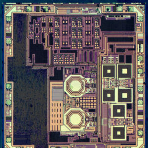
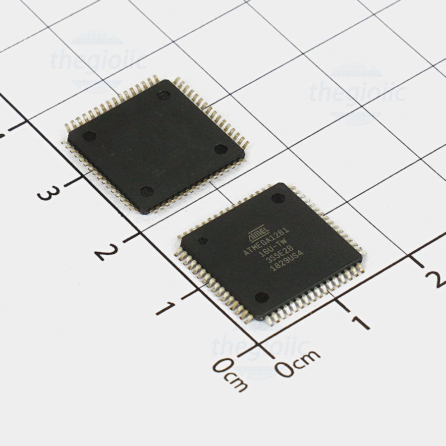
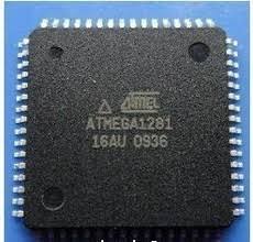
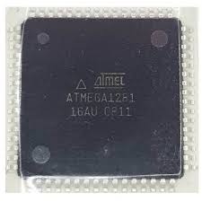
Recover Microprocessor ATmega1281PA Flash
Recover Microprocessor ATmega1281PA Flash heximal file, copy mcu atmega1281pa memory content to new microcontroller and provide the same functions, the security fuse bit of microcontroller atmega1281pa will be cracked reset the status.
The FOCnA/FOCnB/FOCnC bits are only active when the WGMn3:0 bits specifies a non-PWM mode. When writing a logical one to the FOCnA/FOCnB/FOCnC bit, an immediate compare match is forced on the waveform generation unit.
Recover Microprocessor ATmega1281PA Flash heximal file, copy mcu atmega1281pa memory content to new microcontroller and provide the same functions, the security fuse bit of microcontroller atmega1281pa will be cracked reset the status.
The OCnA/OCnB/OCnC output is changed according to its COMnx1:0 bits setting. Note that the FOCnA/FOCnB/FOCnC bits are implemented as strobes. Therefore it is the value present in the COMnx1:0 bits that determine the effect of the forced compare.
A FOCnA/FOCnB/FOCnC strobe will not generate any interrupt nor will it clear the timer in Clear Timer on Compare Match (CTC) mode using OCRnA as TOP before break microcontroller pic16f886.

unlock encrypted mcu atmega1281 microcontroller fuse bit and dump embedded firmware from flash memory and eeprom memory
The two Timer/Counter I/O locations (TCNTnH and TCNTnL, combined TCNTn) give direct access, both for read and for write operations, to the Timer/Counter unit 16-bit counter after Recover MICROPROCESSOR flash.
To ensure that both the high and low bytes are read and written simultaneously when the CPU accesses these registers, the access is performed using an 8-bit temporary High Byte Register (TEMP). This temporary register is shared by all the other 16-bit registers. See “Accessing 16-bit Registers” on page 137.
Modifying the counter (TCNTn) while the counter is running introduces a risk of missing a compare match between TCNTn and one of the OCRnx Registers when attacking dsp mcu texas instrument tms320f2401pg hex.
Writing to the TCNTn Register blocks (removes) the compare match on the following timer clock for all compare units. The Output Compare Registers contain a 16-bit value that is continuously compared with the counter value (TCNTn).
A match can be used to generate an Output Compare interrupt, or to generate a waveform output on the OCnx pin. The Output Compare Registers are 16-bit in size. To ensure that both the high and low bytes are written simultaneously when the CPU writes to these registers, the access is performed using an 8-bit temporary High Byte Register (TEMP).
recover secured microprocessor ATMEGA1281 flash memory and readout mcu embedded firmware from flash program memory and eeprom data memory
This temporary register is shared by all the other 16-bit registers. See “Accessing 16-bit Registers” on page 137. The Input Capture is updated with the counter (TCNTn) value each time an event occurs on the ICPn pin (or optionally on the Analog Comparator output for Timer/Counter1).
The Input Capture can be used for defining the counter TOP value. The Input Capture Register is 16-bit in size. To ensure that both the high and low bytes are read simultaneously when the CPU accesses these registers, the access is performed using an 8-bit temporary High Byte Register (TEMP).
This temporary register is shared by all the other 16-bit registers. See “Accessing 16-bit Registers” on page 137.
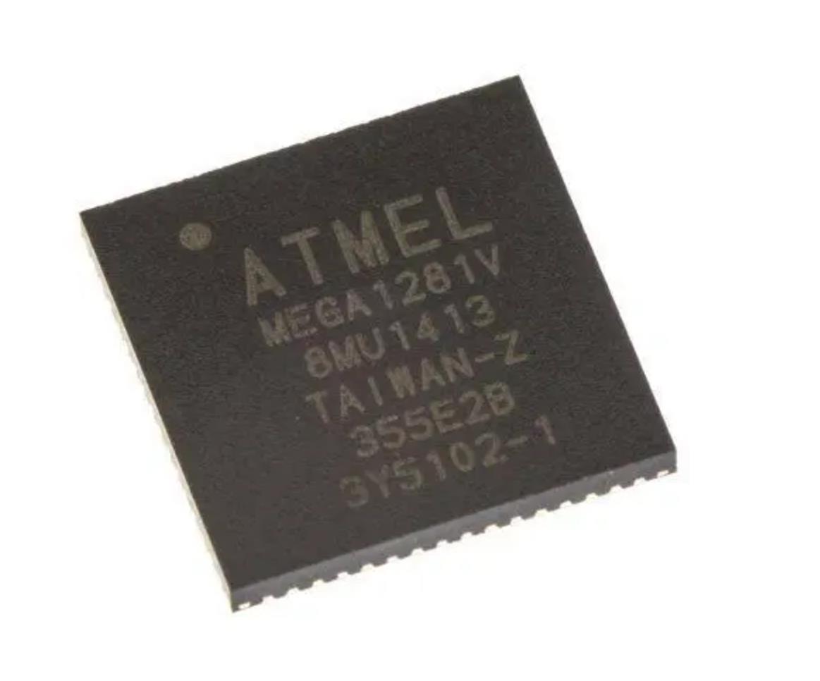
Recover Chip ATmega1281PV Source code
The ATmega1281 is a high-performance 8-bit microcontroller from Microchip’s AVR family, widely used in embedded systems that require reliable operation, low power consumption, and ample memory. It’s found in a range of applications including industrial control, robotics, wireless sensor networks, and automotive electronics. With built-in Flash, EEPROM, SRAM, and advanced protective features like lock bits and secure bootloader mechanisms, it presents a challenge to anyone attempting to recover, clone, or decode its firmware.
ATmega1281 to wydajny 8-bitowy mikrokontroler z rodziny AVR firmy Microchip, szeroko stosowany w systemach wbudowanych wymagających niezawodnej pracy, niskiego zużycia energii i dużej pamięci. Znajduje zastosowanie w wielu zastosowaniach, w tym w sterowaniu przemysłowym, robotyce, sieciach czujników bezprzewodowych i elektronice samochodowej. Dzięki wbudowanej pamięci Flash, EEPROM, SRAM i zaawansowanym funkcjom ochronnym, takim jak bity blokady i mechanizmy bezpiecznego bootloadera, stanowi wyzwanie dla każdego, kto próbuje odzyskać, sklonować lub zdekodować jego oprogramowanie układowe.
W CIRCUIT ENGINEERING CO.,LTD oferujemy zaawansowane usługi inżynierii wstecznej, aby pomóc klientom odzyskać kod źródłowy układu ATmega1281, szczególnie gdy oprogramowanie układowe lub dane programu zostały zablokowane, zaszyfrowane lub w inny sposób zabezpieczone. Niezależnie od tego, czy musisz odblokować, skopiować lub zduplikować plik binarny lub heksametalogowy z układu, zapewniamy rozwiązania na poziomie eksperckim, aby przełamać ochronę.
At CIRCUIT ENGINEERING CO.,LTD, we offer advanced reverse engineering services to help clients recover chip ATmega1281 source code, particularly when the firmware or program data has been locked, encrypted, or otherwise secured. Whether you need to unlock, copy, or duplicate a binary or heximal file from the chip, we provide expert-level solutions to break through the protection.
Recover Chip ATmega1281PV Source code from locked flash memory, copy embedded binary of mcu atmega1281pv to new MCU after crack mcu atmega1281pv fuse bit;
The phase and frequency correct Pulse Width Modulation, or phase and frequency correct PWM mode (WGMn3:0 = 8 or 9) provides a high resolution phase and frequency correct PWM waveform generation option.
The phase and frequency correct PWM mode is, like the phase correct PWM mode, based on a dual-slope operation. The counter counts repeatedly from BOTTOM (0x0000) to TOP and then from TOP to BOTTOM. In non-inverting Compare Output mode, the Output Compare (OCnx) is cleared on the compare match between TCNTn and OCRnx while upcounting, and set on the compare match while downcounting. In inverting Compare Output mode, the operation is inverted if Recover mcu pic16f873 hex.
The dual-slope operation gives a lower maximum operation frequency compared to the single-slope operation. However, due to the symmetric feature of the dualslope PWM modes, these modes are preferred for motor control applications.
hack ATMEGA1281 locked microprocessor fuse bit and copy heximal or binary file from flash program memory or eeprom memory data
The main difference between the phase correct, and the phase and frequency correct PWM mode is the time the OCRnx Register is updated by the OCRnx Buffer Register.
The PWM resolution for the phase and frequency correct PWM mode can be defined by either ICRn or OCRnA. The minimum resolution allowed is 2-bit (ICRn or OCRnA set to 0x0003), and the maximum resolution is 16-bit (ICRn or OCRnA set to MAX) after Recover tms320f2812pgfa microcontroller firmware.
The PWM resolution in bits can be calculated using the following equation: In phase and frequency correct PWM mode the counter is incremented until the counter value matches either the value in ICRn (WGMn3:0 = 8), or the value in OCRnA (WGMn3:0 = 9).
The counter has then reached the TOP and changes the count direction. The TCNTn value will be equal to TOP for one timer clock cycle. The timing diagram for the phase correct and frequency correct PWM mode is shown on Figure 57 if break microcontroller pic16f767 firmware.
Step-by-Step Procedure to Recover ATmega1281 Firmware
-
Chip Analysis & Protection Detection
We begin by identifying the protection mechanisms in place. The ATmega1281 supports several levels of code protection (e.g., LB1/LB2 lock bits). We use non-invasive or semi-invasive techniques to detect these protections before attempting any attack. -
Memory Dumping & Flash Extraction
Using advanced hardware programmers and glitching techniques (such as clock glitching or power analysis), we attempt to crack or hack into the device to dump the flash and EEPROM memory contents. -
Binary Firmware Extraction
Once we successfully access the chip, the firmware, typically in binary or hex format, is extracted. This step requires careful handling to avoid triggering security self-erasure or bricking the device. -
Firmware Decryption (If Encrypted)
If the firmware or data archive is encrypted, we deploy side-channel analysis or cryptographic pattern detection to decrypt the content. Our team may utilize signal timing analysis, fault injection, or brute-force cracking methods depending on the complexity. -
Disassembly and Source Code Recovery
The heximal data is then disassembled into assembly code, and with advanced decompilation tools, we restore it to a human-readable C/C++ source code as accurately as possible. -
Verification and Code Reconstruction
Finally, we analyze the functionality of the recovered program, reconstruct missing logic where necessary, and verify it against the original system behavior for accuracy.
The figure shows phase and frequency correct PWM mode when OCRnA or ICRn is used to define TOP. The TCNTn value is in the timing diagram shown as a histogram for illustrating the dual-slope operation. The diagram includes non-inverted and inverted PWM outputs.
ATmega1281, Microchip’in AVR ailesinden yüksek performanslı 8 bitlik bir mikrodenetleyicidir ve güvenilir çalışma, düşük güç tüketimi ve bol bellek gerektiren gömülü sistemlerde yaygın olarak kullanılır. Endüstriyel kontrol, robotik, kablosuz sensör ağları ve otomotiv elektroniği gibi çeşitli uygulamalarda bulunur. Dahili Flash, EEPROM, SRAM ve kilit bitleri ve güvenli önyükleyici mekanizmaları gibi gelişmiş koruyucu özelliklerle, aygıt yazılımını kurtarmaya, klonlamaya veya kodunu çözmeye çalışan herkes için bir zorluk teşkil eder.
CIRCUIT ENGINEERING CO.,LTD’de, özellikle aygıt yazılımı veya program verileri kilitlendiğinde, şifrelendiğinde veya başka bir şekilde güvenli hale getirildiğinde, müşterilerin çip ATmega1281 kaynak kodunu kurtarmalarına yardımcı olmak için gelişmiş tersine mühendislik hizmetleri sunuyoruz. Çipten ikili veya altıgen bir dosyayı kilidini açmanız, kopyalamanız veya çoğaltmanız gerekip gerekmediğine bakılmaksızın, korumayı aşmak için uzman düzeyinde çözümler sunuyoruz.
The small horizontal line marks on the TCNTn slopes represent compare matches between OCRnx and TCNTn. The OCnx Interrupt Flag will be set when a compare match occurs.
Applications and Unique Features of the ATmega1281
The ATmega1281 stands out for its 128KB of self-programmable Flash memory, 4KB of EEPROM, and 8KB of SRAM. Its 86 general-purpose I/O lines, internal oscillator, and robust peripheral set (SPI, I2C, UART, ADC, timers) make it ideal for sophisticated embedded control systems.
It is commonly used in:
-
Wireless mesh networking (Zigbee-based applications)
-
Industrial machine controllers
-
Data loggers and smart meters
-
Home automation and security devices
-
Custom automotive ECUs
These applications often require post-deployment updates or forensic analysis, which is only possible by accessing the secured firmware. That’s where our chip unlocking services come in.

ATmega1281 — это высокопроизводительный 8-битный микроконтроллер из семейства AVR компании Microchip, широко используемый во встраиваемых системах, которым требуется надежная работа, низкое энергопотребление и большой объем памяти. Он используется в различных приложениях, включая промышленное управление, робототехнику, беспроводные сенсорные сети и автомобильную электронику. Благодаря встроенной флэш-памяти, EEPROM, SRAM и расширенным защитным функциям, таким как биты блокировки и защищенные механизмы загрузчика, он представляет собой сложную задачу для любого, кто пытается восстановить, клонировать или декодировать его прошивку.
В CIRCUIT ENGINEERING CO.,LTD мы предлагаем расширенные услуги обратного инжиниринга, чтобы помочь клиентам восстановить исходный код чипа ATmega1281, особенно когда данные прошивки или программы были заблокированы, зашифрованы или иным образом защищены. Если вам нужно разблокировать, скопировать или дублировать двоичный или шестнадцатеричный файл с чипа, мы предоставляем экспертные решения для взлома защиты.
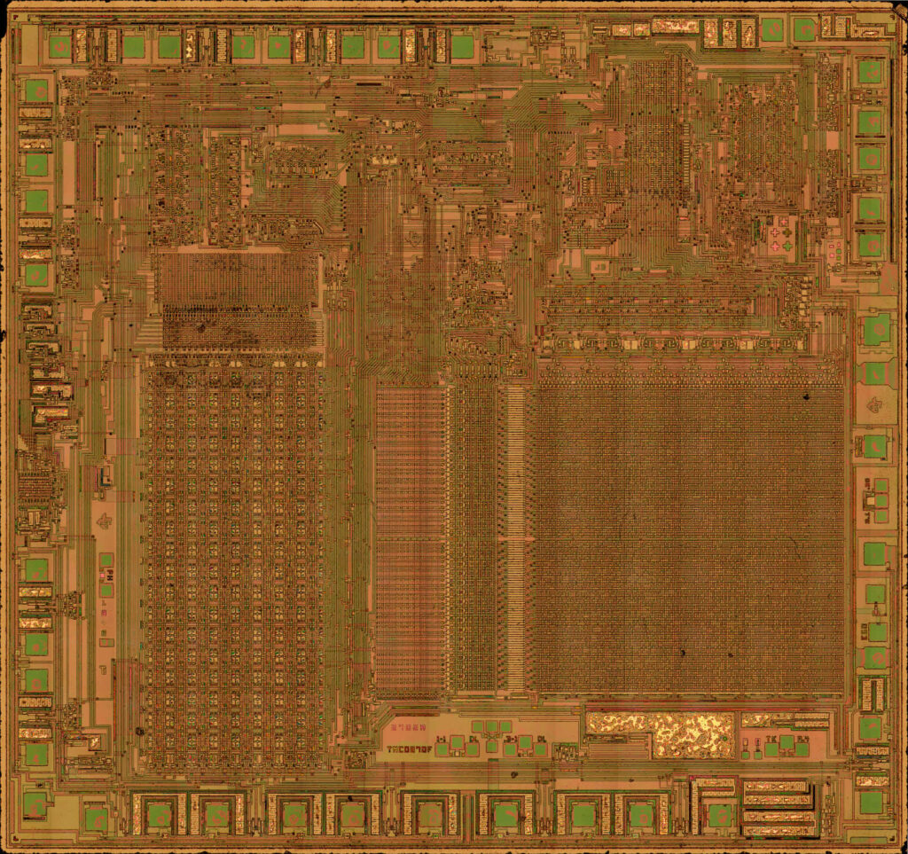
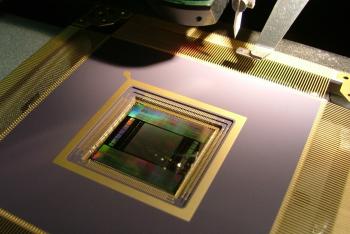
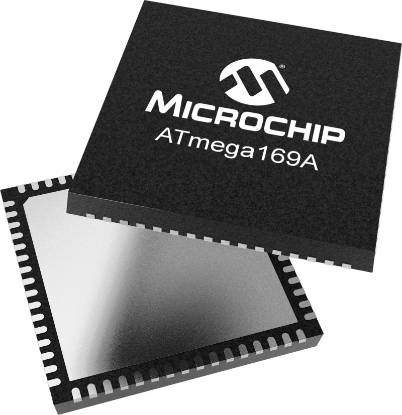
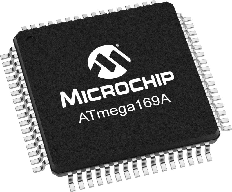
Reverse Engineering Microcontroller ATmega169A Binary
Reverse Engineering Microcontroller ATmega169A and copy mcu atmega169a Binary from its flash and eeprom memory, the tamper resistance system of microcontroller atmega169a will be unlocked;
When changing the TOP value the program must ensure that the new TOP value is higher or equal to the value of all of the Compare Registers.
If the TOP value is lower than any of the Compare Registers, a compare match will never occur between the TCNTn and the OCRnx. Note that when using fixed TOP values, the unused bits are masked to zero when any of the OCRnx Registers are written if attack pic18f66k90 MICROCONTROLLER memory.
As the third period shown in Figure 56 illustrates, changing the TOP actively while the Timer/Counter is running in the phase correct mode can result in an unsymmetrical output. The reason for this can be found in the time of update of the OCRnx Register.
Since the OCRnx update occurs at TOP, the PWM period starts and ends at TOP. This implies that the length of the falling slope is determined by the previous TOP value, while the length of the rising slope is determined by the new TOP value.
When these two values differ the two slopes of the period will differ in length. The difference in length gives the unsymmetrical result on the output.
crack ATmega169a microcomputer fuse bit and readout firmware program from flash of ATmega169a microcontroller
It is recommended to use the phase and frequency correct mode instead of the phase correct mode when changing the TOP value while the Timer/Counter is running. When using a static TOP value there are practically no differences between the two modes of operation when recover mc9s08dz32 MICROCONTROLLER embedded firmware.
In phase correct PWM mode, the compare units allow generation of PWM waveforms on the OCnx pins. Setting the COMnx1:0 bits to two will produce a non-inverted PWM and an inverted PWM output can be generated by setting the COMnx1:0 to three.
The actual OCnx value will only be visible on the port pin if the data direction for the port pin is set as output (DDR_OCnx). The PWM waveform is generated by setting (or clearing) the OCnx Register at the compare match between OCRnx and TCNTn when the counter increments, and clearing (or setting) the OCnx Register at compare match between OCRnx and TCNTn when the counter decrements.
The PWM frequency for the output when using phase correct PWM can be calculated by the following equation:
The N variable represents the prescaler divider (1, 8, 64, 256, or 1024). The extreme values for the OCRnx Register represent special cases when generating a PWM waveform output in the phase correct PWM mode.
unlock atmega169a microprocessor fuse bit and extract source code from flash memory of atmega169a mcu
If the OCRnx is set equal to BOTTOM the output will be continuously low and if set equal to TOP the output will be continuously high for non-inverted PWM mode.
For inverted PWM the output will have the opposite logic values. If OCR1A is used to define the TOP value (WGM13:0 = 11) and COM1A1:0 = 1, the OC1A output will toggle with a 50% duty cycle.
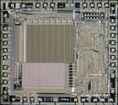
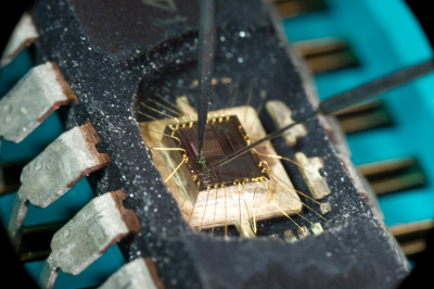
Recover MCU PIC16F74A Binary
Recover MCU PIC16F74A Binary from embedded flash and eeprom memory, extract the firmware from microcontroller pic16f74a needs to copy program to new microcontroller.
The high performance of the PIC16CXX family can be attributed to a number of architectural features commonly found in RISC microprocessors. To begin with, the PIC16CXX uses a Harvard architecture, in which, program and data are accessed from separate memories using separate buses.
This improves bandwidth over traditional von Neumann architecture in which program and data are fetched from the same memory using the same bus. Separating program and data buses further allows instructions to be sized differently than the 8-bit wide data word after break mc9s12xdg128 MCU.
Instruction opcodes are 14-bits wide making it possible to have all single word instructions. A 14-bit wide program memory access bus fetches a 14-bit instruction in a single cycle. A two-stage pipeline overlaps fetch and execution of instructions (Example 3-1). Consequently, all instructions (35) execute in a single cycle (200 ns @ 20 MHz) except for program branches if break atmega128a MCU flash.
The PIC16CXX can directly or indirectly address its register files or data memory. All special function registers, including the program counter, are mapped in the data memory. The PIC16CXX has an orthogonal (symmetrical) instruction set that makes it possible to carry out any operation on any register using any addressing mode. This symmetrical nature and lack of ‘special optimal situations’ make programming with the PIC16CXX simple yet efficient. In addition, the learning curve is reduced significantly.
PIC16CXX devices contain an 8-bit ALU and working register. The ALU is a general purpose arithmetic unit. It performs arithmetic and Boolean functions between the data in the working register and any register file if Recover MCU. The ALU is 8-bits wide and capable of addition, subtraction, shift and logical operations. Unless otherwise mentioned, arithmetic operations are two’s complement in nature. In two-operand instructions, typically one operand is the working register (W register). The other operand is a file register or an immediate constant. In single operand instructions, the operand is either the W register or a file register.
crack pic16f74a microcontroller protection and readout pic16f74a mcu chip program from flash memory
The W register is an 8-bit working register used for ALU operations. It is not an addressable register.
Depending on the instruction executed, the ALU may affect the values of the Carry (C), Digit Carry (DC), and Zero (Z) bits in the STATUS register. The C and DC bits operate as a borrow bit and a digit borrow out bit, respectively, in subtraction. See theSUBLW and SUBWF instructions for examples.