Posts Tagged ‘break locked chip memory’
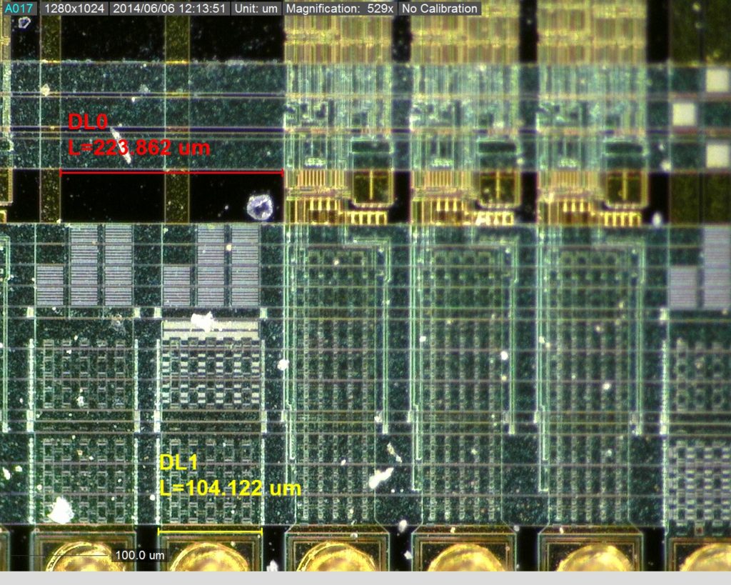
 Break Locked Chip PIC16F74 Data
Break Locked Chip PIC16F74 program memory and readout MCU Data from eeprom memory, the heximal file can be rewritten to the new microcontroller PIC16F74 for IC cloning;
If the data protection bit has not been programmed, the on-chip program memory can be read out for verification process. The first 64 locations can be read by the PIC16F74 regardless of the data protection bit setting.
The last memory location cannot be read if data protection is enabled on the PIC16F74. The last memory location can be read regardless of the data protection bit setting on the PIC16F74 if recover microprocessor atmega1281pa flash.
Four memory locations are designated as ID locations where the user can store checksum or other data-identification numbers. These locations are not accessible during normal execution but are readable and writable during program/verify.
Use only the lower 4 bits of the ID locations and always program the upper 8 bits as ’0’s. The PIC16F74 locked chips with EPROM program memory can be serially programmed while in the end application circuit before Break ic atmega2560pa heximal.
This is simply done with two lines for clock and data, and three other lines for power, ground, and the programming voltage. This allows customers to manufacture boards with unprogrammed devices, and then program the locked chip just before shipping the product.
This also allows the most recent firmware or a custom firmware to be programmed. The device is placed into a program/verify mode by holding the GP1 and GP0 pins low while raising the MCLR (VPP) pin from VIL to VIHH (see programming specification).
GP1 becomes the programming clock and GP0 becomes the programming data. Both GP1 and GP0 are Schmitt Trigger inputs in this mode if Break mcu atmega2560l flash.
After reset, a 6-bit command is then supplied to the device. Depending on the command, 14-bits of program data are then supplied to or from the device, depending if the command was a load or a read. For complete details of serial programming, please refer to the PIC12C5XX Programming Specifications. A typical in-circuit serial programming connection is shown in Figure 8-16.