Archive for the ‘Break IC’ Category
 Break MCU Firmware
 September 13th, 2012 |
  Author:
 Non-invasive Break MCU Firmware are particularly dangerous in some applications for two reasons. Firstly, the owner of the device might not notice that the secret keys or data have been stolen, therefore it is unlikely that the validity of the compromised keys will be revoked before they are abused.
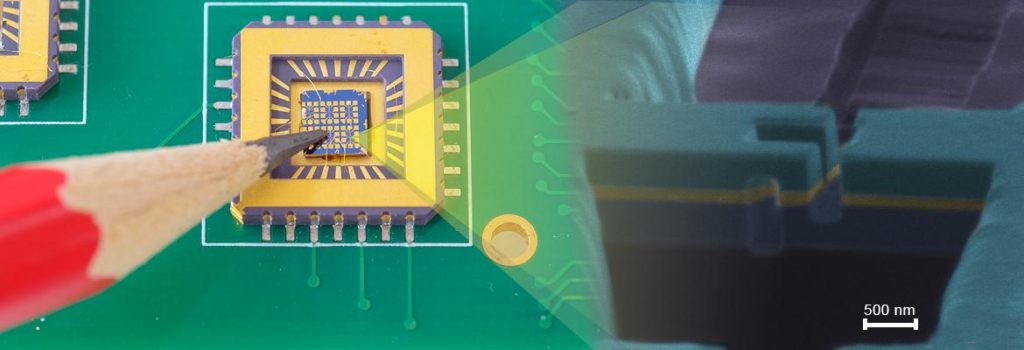
Secondly, non-invasive Microcontroller unlocking often scale well, as the necessary equipment can usually be reproduced and updated at low cost.
The design of most non-invasive ic cracks requires detailed knowledge of both the processor and software. On the other hand, invasive microprobing MCU reading require very little initial knowledge and usually work with a similar set of techniques on a wide range of products.
Attacks therefore often start with invasive reverse engineering, the results of which then help to develop cheaper and faster non-invasive attacks. Semi-invasive IC flash breaking can be used to learn the device functionality and test its security circuits. As these mcu cracks do not require establishing any physical contact to the internal chip layers, expensive equipment such as laser cutters and FIB machines are not required. The mcu firmware breaker could succeed using a simple off-the-shelf microscope with a photoflash or laser pointer attached to it.
 Posted in Break IC |
  Tags: cpld firmware break, dsp firmware break, eeprom firmware break, flash eeprom firmware break, fpga firmware break, fram firmware break, mask rom firmware break, mram firmware break, nvram firmware break, otp eprom firmware break, pld firmware break, sram firmware break, static ram firmware break, uv eprom firmware break |
  Comments Closed
Attack MCU Firmware
Attack MCU Firmware is actually a process of decapsulate the silicon package of microcontroller and disable its fuse bit by focus ion beam, then extract code from MCU flash memory;
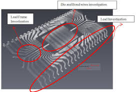
All microprobing and reverse engineering microcontroller techniques are invasive mcu firmware attacks. They require hours or weeks in specialised laboratory and in the process they destroy the packaging.
The other three are non-invasive mcu cracking methods. The microprocessor code extracting device is not physically harmed during these ic cracks. The last MCU breaking category could also be semi-invasive. It means that the access to the chip’s die is required but the attack is not penetrative and the fault is generated with intensive light pulse, radiation, local heating or other means.
Posted in Break IC |
Tags: cpld firmware attack, dsp firmware attack, eeprom firmware attack, flash eeprom firmware attack, fpga firmware attack, fram firmware attack, mask rom firmware attack, mram firmware attack, nvram firmware attack, otp eprom firmware attack, pld firmware attack, sram firmware attack, static ram firmware attack, uv eprom firmware attack |
Comments Closed
Break Chip Microprocessor ATXMEGA192A1 Eeprom
We can break Chip Microprocessor ATXMEGA192A1 Eeprom, please view the Chip Microprocessor ATXMEGA192A1 features for your reference:
The User Signature Row is a seperate memory section that is fully accessible (read and write) from application software and external programming. The User Signature Row is one flash page in size, and is meant for static user parameter storage, such as calibration data, custom serial numbers, random number seeds etc. This section is not erased by Chip Erase, and requires a dedicated erase command. This ensures parameter storage during multiple program/erase session and On-Chip Debug sessions after the eeprom of chip being break.
The Flash Program Memory and EEPROM data memory is organized in pages. The pages are word accessible for the Flash and byte accessible for the EEPROM.
Table 7-2 on page 14 shows the Flash Program Memory organization. Flash write and erase operations are performed on one page at the time, while reading the Flash is done one byte at the time. For Flash access the Z-pointer (Z[m:n]) is used for addressing.
The most significant bits in the address (FPAGE) gives the page number and the least significant address bits (FWORD) gives the word in the page. Table 7-3 on page 14 shows EEPROM memory organization for the XMEGA A1 devices.
EEPROM write and erase operations can be performed one page or one byte at the time, while reading the EEPROM is done one byte at the time. For EEPROM access the NVM Address Register (ADDR[m:n]) is used for addressing. The most significant bits in the address (E2PAGE) gives the page number and the least significant address bits (E2BYTE) gives the byte in the page before breaking eeprom of microprocessor.
Allows High-speed data transfer
– From memory to peripheral
– From memory to memory
– From peripheral to memory
– From peripheral to peripheral
4 Channels
From 1 byte and up to 16M bytes transfers in a single transaction when BREAK IC
Multiple addressing modes for source and destination address
– Increment
– Decrement
– Static
1, 2, 4, or 8 byte Burst Transfers
Programmable priority between channels
Crack MCU Firmware
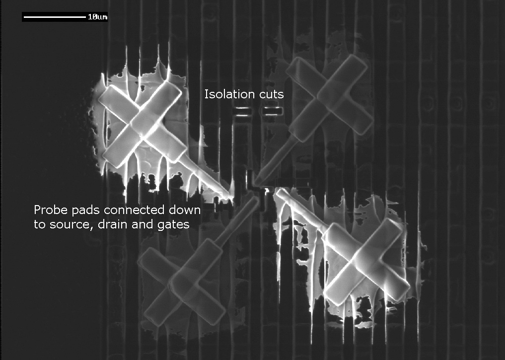
The next improvement to hardware security protection was done by embedding the fuse area into the main memory array so that it shares some of the control or data lines. This implementation is more secure because the fuses are part of the memory array and their localisation is very difficult and challenging task. Fuses can share word-lines with the main memory, for example, as in the Hitachi HD6473048 microcontroller MCU;
or they can share bit-lines as in the Holtek HT48R50A microcontroller MCU. In the latter implementation the fuses do not have a separate bit-lines that for attacking MCU firmware. But that does not mean it will be more secure because the state of the fuses cannot be monitored all the time and usually is sampled at power-up and stored in a separate register.
A high level of security can be achieved if a certain memory location is used as a security fuse. In this case it would be extremely difficult to find this location and reset it without disturbing the contents of other memory cells. That does not mean that other mcu code extraction methods will not work, such as, non-invasive mcu firmware crack, but at least this reduces the chance of success with simple semi-invasive microcontroller unlocking.
 Posted in Break IC |
Tags: cpld mcu firmware crack, dsp mcu firmware crack, eeprom mcu firmware crack, flash eeprom mcu firmware crack, fpga mcu firmware crack, fram mcu firmware crack, mask rom mcu firmware crack, mram mcu firmware crack, nvram mcu firmware crack, otp eprom mcu firmware crack, pld mcu firmware crack, sram mcu firmware crack, static ram mcu firmware crack, uv, uv eprom mcu firmware crack |
Comments Closed
Posted in Break IC |
Tags: cpld mcu firmware crack, dsp mcu firmware crack, eeprom mcu firmware crack, flash eeprom mcu firmware crack, fpga mcu firmware crack, fram mcu firmware crack, mask rom mcu firmware crack, mram mcu firmware crack, nvram mcu firmware crack, otp eprom mcu firmware crack, pld mcu firmware crack, sram mcu firmware crack, static ram mcu firmware crack, uv, uv eprom mcu firmware crack |
Comments Closed
Copy MCU Firmware
Copy MCU Firmware in the format of binary or heximal, and copy the code to new Microcontroller, the status of Microprocessor will be reset to unlocked one;
Most MCU microcontrollers on the market have a security fuse (or multiple fuses) that control access to the information stored in on-chip memory. These fuses could be implemented in software or in hardware.
Software implementation means that a password is stored in the memory or a certain memory location is assigned as a security fuse. For example, in the Motorola MC68HC908 family, password protection is used, and in the Motorola MC68HC705B family, the security fuse is located in the first byte of the data EEPROM memory.
Both variants have relatively high security, because it is extremely difficult to find the physical location of the fuse or password and reset them. At the same time, people want to copy IC program can try using glitch to override the security check subroutine, or use power analysis to see whether a password guess is correct or not.
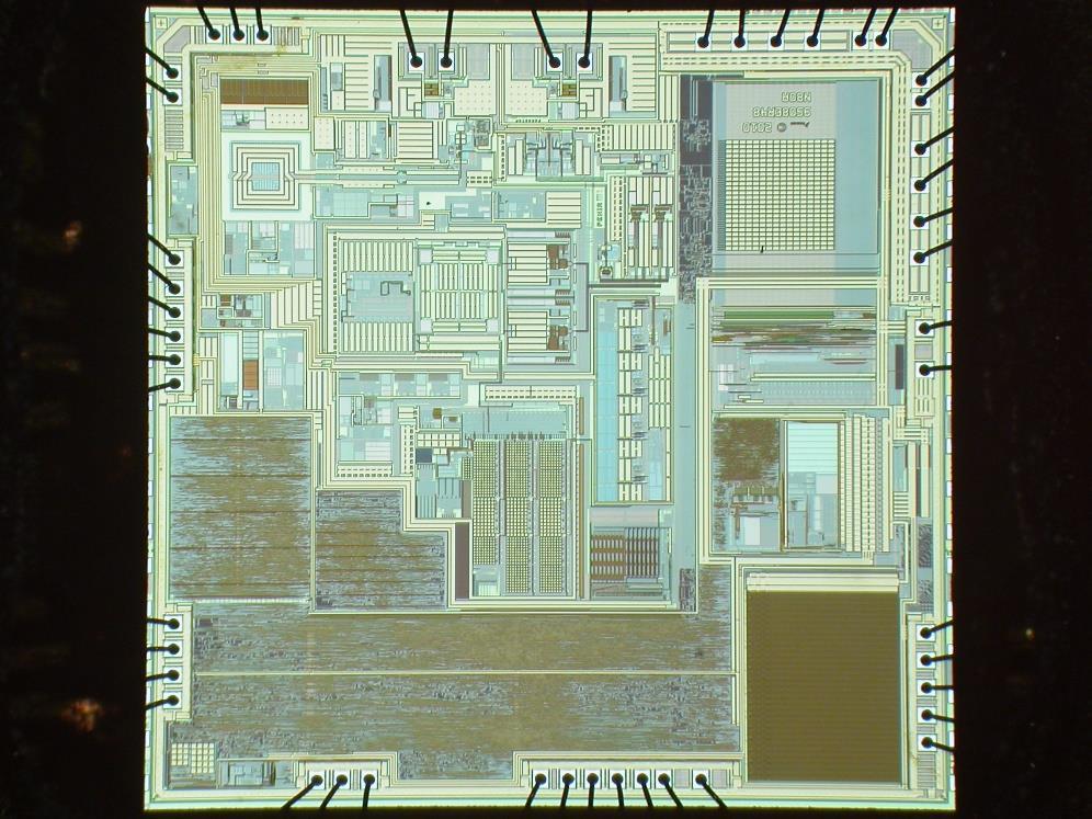
In hardware implementation, security fuses are physically located on the chip die. This could mean a separate memory cell located next to the main memory array, or even far from it. For example, this is the case for all Microchip PIC MCU and Atmel AVR MCU. In both cases, the security is not very high as the fuses can be easily found and disabled by one or another method. Meantime, some methods require very expensive equipment and even if the people who want to break MCU processor knows where the fuse is, he will not be able to reset it until he gets access to such equipment and learns how to use it.
 Posted in Break IC |
Tags: chip firmware copy, cpld mcu firmware copy, dsp mcu firmware copy, eeprom mcu firmware copy, flash eeprom mcu firmware copy, fpga mcu firmware copy, fram mcu firmware copy, ic firmware copy, mask rom mcu firmware copy, mram mcu firmware copy, nvram mcu firmware copy, otp eprom mcu firmware copy, pld mcu firmware copy, sram mcu firmware copy, static ram mcu firmware copy, uv eprom mcu firmware copy |
Comments Closed
Posted in Break IC |
Tags: chip firmware copy, cpld mcu firmware copy, dsp mcu firmware copy, eeprom mcu firmware copy, flash eeprom mcu firmware copy, fpga mcu firmware copy, fram mcu firmware copy, ic firmware copy, mask rom mcu firmware copy, mram mcu firmware copy, nvram mcu firmware copy, otp eprom mcu firmware copy, pld mcu firmware copy, sram mcu firmware copy, static ram mcu firmware copy, uv eprom mcu firmware copy |
Comments Closed
Extract MCU Firmware
Extract MCU Firmware from program memory and data memory after remove the tamper resistance system of microcontroller and replicate the code to new MCU;
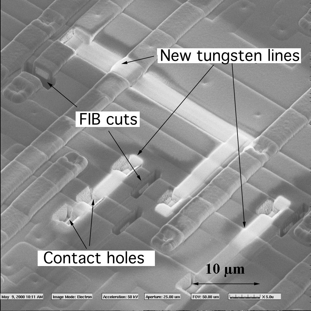
Some manufacturers intentionally do not provide any programming specifications for their MCU microcontrollers. That does not give very good protection on its own, and only slightly increases the cost of microcontroller reverse engineering, because this MCU firmware can be extracted by observing the signals applied to the IC chip during programming in a development kit or in a universal programmer.
Obviously, for the highest security, the system would not have any programming interface at all, and would not provide any access to stored data. This is normally the case for Mask ROM microcontrollers and smartcards. The only practical ways of attack chip flash in this case would be either to microprobe the data bus to recover the information or use power analysis and glitch attacks to exploit any vulnerability in software.
Relatively high security can be obtained when a microcontroller is user programmable but does not provide any read-back facility – only verify and write check, for example in the NEC 78K0S family Flash microcontrollers.
Of course this should be implemented properly to avoid the situation where the microprocessor decryption can force the system to verify one byte at a time. In this case he would need on average 128 attempts per byte (28 × 0.5) and assuming the byte access cycle is 5 ms it will take him less than a day to extract the contents of the memory, which is usually between 4 Kb and 64 Kb. Even if the verify operation is applied to large blocks of data, the mcu firmware extraction could try glitch attacks to reduce the cycle to a single byte.
Posted in Break IC |
Tags: cpld mcu firmware extract, dsp mcu firmware extract, eeprom mcu firmware extract, extract ic firmware, flash eeprom mcu firmware extract, fpga mcu firmware extract, fram mcu firmware extract, mask rom mcu firmware extract, mram mcu firmware extract, nvram, otp eprom mcu firmware extract, pld mcu firmware extract, sram mcu firmware extract, static ram mcu firmware extract, uv eprom mcu firmware extract |
Comments Closed
Read MCU Code
Read MCU Code out from embedded and secured flash memory and eeprom memory can help to recover the content from master microcontroller;
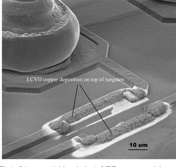
Another memory type used in all Microcontroller MCUs (mainly as a register file memory and operational memory) is SRAM. It is also used in secure microcontroller MCUs such as the Dallas DS5002FP and JAVA iButtons where the information should disappear quickly if atampering attempt is sensed. An SRAM memory cell consists of six transistors, four of which create a flip-flop while the other two are used for accessing the cell inside the array.
SRAM memory offers very good security protection, as the information from it can be easily erased by disconnecting the power supply if the alarm is triggered. Performing invasive or semi-invasive MCU Crack is very problematic because any attempt to extract microcontroller code surface would very likely destroy the data. For example, decapsulation requires very strong acids to be used which a
re conductive and cannot be used on a powered up chip. Even if chip atmega2561v attacker manages to access the die, the state of its transistors cannot be observed optically. Microprobing is difficult because the internal wires are buried under top metal bit-lines, ground and power supply wires. The only practical way to access the memory is from the rear side of the chip die, but this requires more expensive equipment and a highly skilled IC Attacker.
Meantime, there are some semi-invasive techniques that allow observation of the memory state, but require special laser scanning microscopes. At the same time non-invasive mcu attacks can be used to exploit any problems that might exist in the memory interface, as happened with the Dallas Semiconductor secure microcontrolle.
Data remanence could cause some problems to SRAM security as well. At temperatures below 0˚C some samples of the SRAM chips retain information for hours. But, in general, SRAM memory offers a very good level of protection and low-temperature attacks can be avoided by placing temperature sensors into the secure module enclosure as in the IBM 4758 cryptoprocessor.
Posted in Break IC |
Tags: cpld mcu source code read, dsp, dsp mcu source code read, eeprom mcu source code read, flash eeprom, fpga mcu source code read, fram mcu source code read, mask rom mcu source code read, mram mcu source code read, nvram mcu source code read, otp ram mcu source code read, pld mcu source code read, sram mcu source code read, static ram mcu source code read, uv eprom mcu source code read |
Comments Closed
Break Secured IC PIC16F716 Firmware
Break Secured IC PIC16F716 flash memory, cut off microcontroller PIC16F716 security fuse bit and extract firmware from MCU.
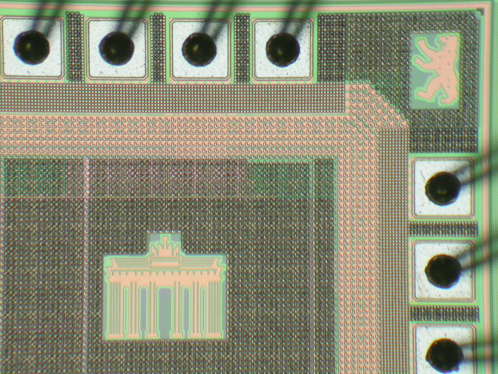
The PIC16F7X devices have a 13-bit program counter capable of addressing an 8K word x 14-bit program memory space. The PIC16F77/76 devices have 8K words of FLASH program memory and the PIC16F73/74 devices have 4K words when copy ic atmega8l heximal.
The program memory maps for PIC16F7X devices are shown in Figure 2-1. Accessing a location above the physically implemented address will cause a wrap around Firmware.
The RESET Vector is at 0000h and the Interrupt Vector is at 0004h. The Data Memory is partitioned into multiple banks, which contain the General Purpose Registers and the Special Function Registers.
Bits RP1 (STATUS<6>) and RP0 (STATUS<5>) are the bank select bits: Each bank extends up to 7Fh (128 bytes). The lower locations of each bank are reserved for the Special Function Registers after copy mcu pic32mx440f512 bin.
Above the Special Function Registers are General Purpose Registers, implemented as static RAM. All implemented banks contain Special Function Registers.
Some frequently used Special Function Registers from one bank may be mirrored in another bank for firmware reduction and quicker access. The register file (shown in Figure 2-2 and Figure 2-3) can be accessed either directly, or indirectly, through the File Select Register FSR Firmware.
The Special Function Registers are registers used by the CPU and peripheral modules for controlling the desired operation of the device. These registers are implemented as static RAM after IC breaking.
The Special Function Registers can be classified into two sets: core (CPU) and peripheral. Those registers associated with the core functions are described in detail in this section. Those related to the operation of the peripheral features are described in detail in the peripheral feature section.
MCU Code Restoration
MCU Code Restoration can help engineer to recover mcu heximal from secured memory include flash and eeprom one after crack microcontroller;
Another big problem for EPROM, EEPROM and Flash memories that affects the hardware security of the MCU devices is data remanence. Many MCUs with these types of memory have a security fuse which, once activated, cannot be reset until the whole memory content is first erased. Manufacturers put a lot of effort into hardware design to ensure that the security fuse will not be deactivated by manipulation of external signals such as power glitches. They made very good progress, and very few of the modern MCUs can be broken using tricks such as applying power glitches during the chip erase operation to terminate the memory erase without affecting the erase of the security fuse, or exposing the chip to UV light for long enough to erase the security fuse but not long enough to destroy the memory source code contents.
But recent revisions of MCUs are not sensitive to such IC code extraction. In modern chips, an additional voltage monitoring circuit is usually implemented, causing a reset of the hardware programming interface or preventing any write/erase operations below or above certain voltages. What was wrongly assumed is that information must disappear from the memory after it was erased. In fact some traces of the data are still left after the erase operation, and to get the information back we just have to find the right method to measure the residual charge on a floating gate, or a threshold of a memory transistor.
This is not an easy task, but if the security fuse was deactivated during the chip erase operation, the memory can be accessed normally. That allows engineer to recover ic eeprom program and measure the response from each transistor inside the array by sequential reading of each memory location and microprobing the internal memory bus.
Of course it is not a trivial task, but a determined and experienced mcu program breaker can do this. In some MCUs the threshold level of each transistor can be measured in fully non-invasive mcu code restoration way by playing with the interface and power supply voltages. This is possible because very often the memory sense circuit uses the power supply voltage as a reference.
EPROM advantage when MCU Code Decryption
MCU Code Decryption happens after extract microcontroller heximal file out from its embedded program and data memory through unlock MCU method;
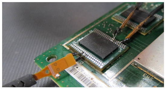
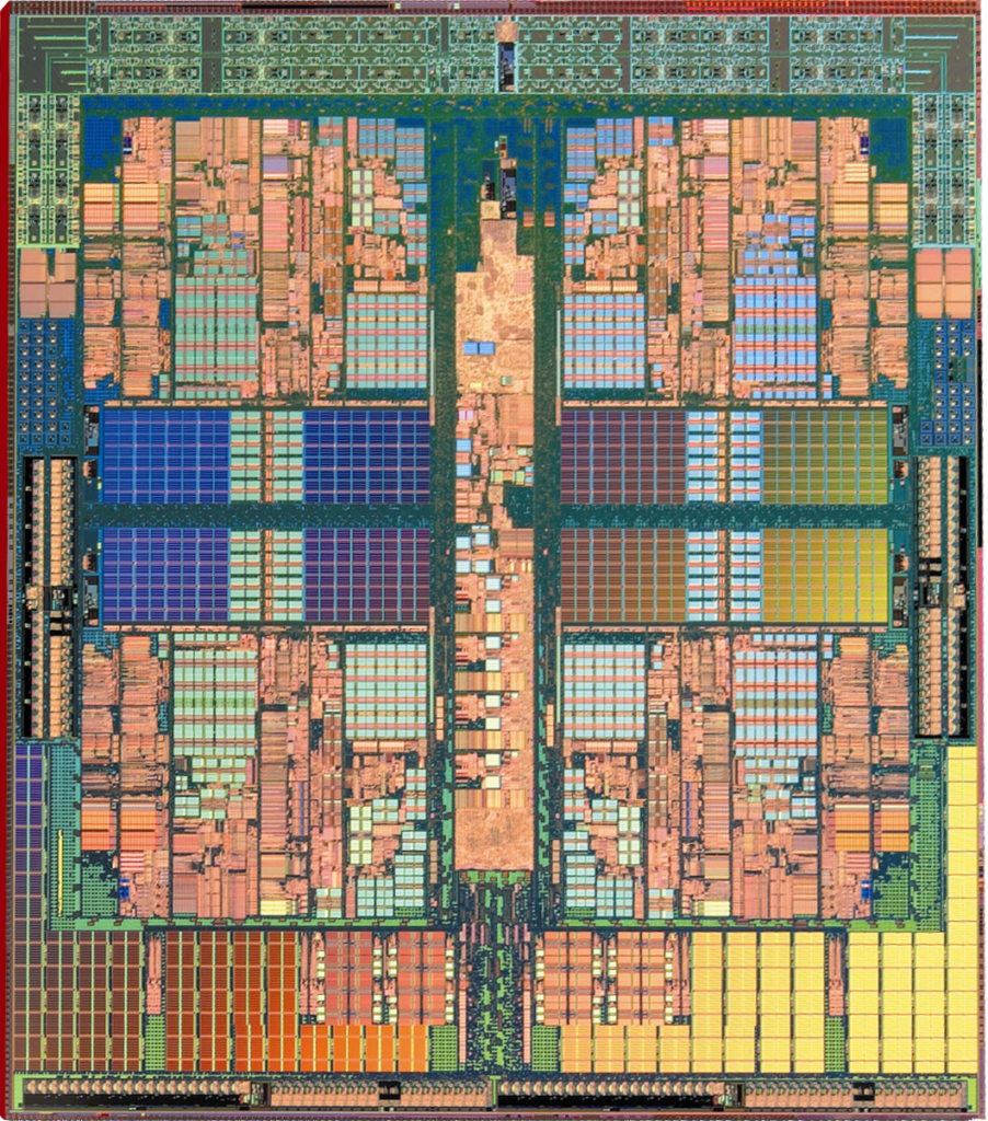
In terms of non-invasive MCU Code Decryption, EPROM memory has some advantages over EEPROM and Flash memories as it is more robust against power glitch decryptions. This happens because it has a simpler structure, larger cell size, thicker gate oxide and no on-chip high-voltage charge pumps.
The sense amplifiers used to distinguish between ‘0’ and ‘1’ logic states are much simpler in EPROM and less sensitive to the power supply voltage. Against semi-invasive mcu source code decryption, EPROM memory is also better than EEPROM and Flash. For example, the fault injection decryption that will be discussed later can be used to modify the contents of the cell but for EPROM much higher power is required.
That makes OTP microcontrollers more attractive in the applications where high security is required. Unfortunately modern microcontrollers do not use this type of memory any more as it cannot be reprogrammed, has lower density than the Flash memory and is thus more expensive. That forces semiconductor manufacturers to introduce additional protection against unauthorised access to the memory contents.
For example, modern smartcards do not have hardware control for access to the on-chip Flash and EERPOM memories, but only a bootstrap loader located in the Flash memory that overwrites itself during first initialisation, eliminating any possible access to the information (unless implemented by the customer). Hardware access to the memory has multi-level security protection ensuring that access will not be granted unless all the requirements are met. In some microcontrollers, very sophisticated access password protection is implemented.
Posted in Break IC |
Tags: cpld mcu source code decryption, dsp mcu source code decryption, eeprom source code decryption, eprom source code decryption, fpga mcu source code decryption, pld mcu source code decryption |
Comments Closed