Archive for July, 2014
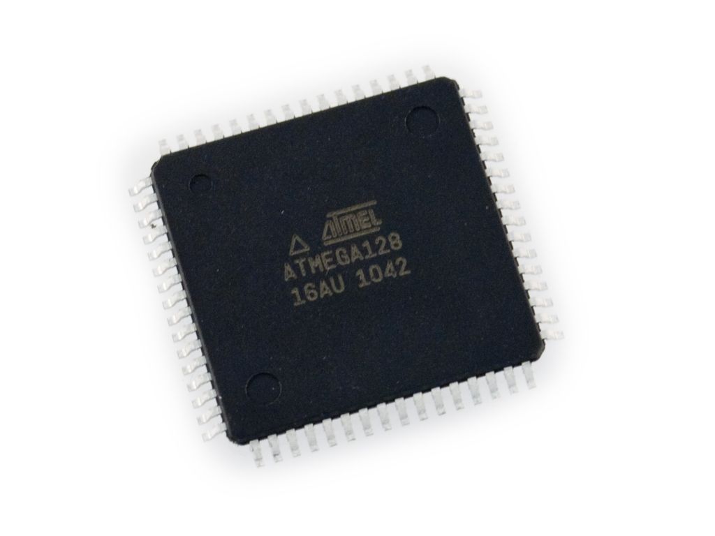
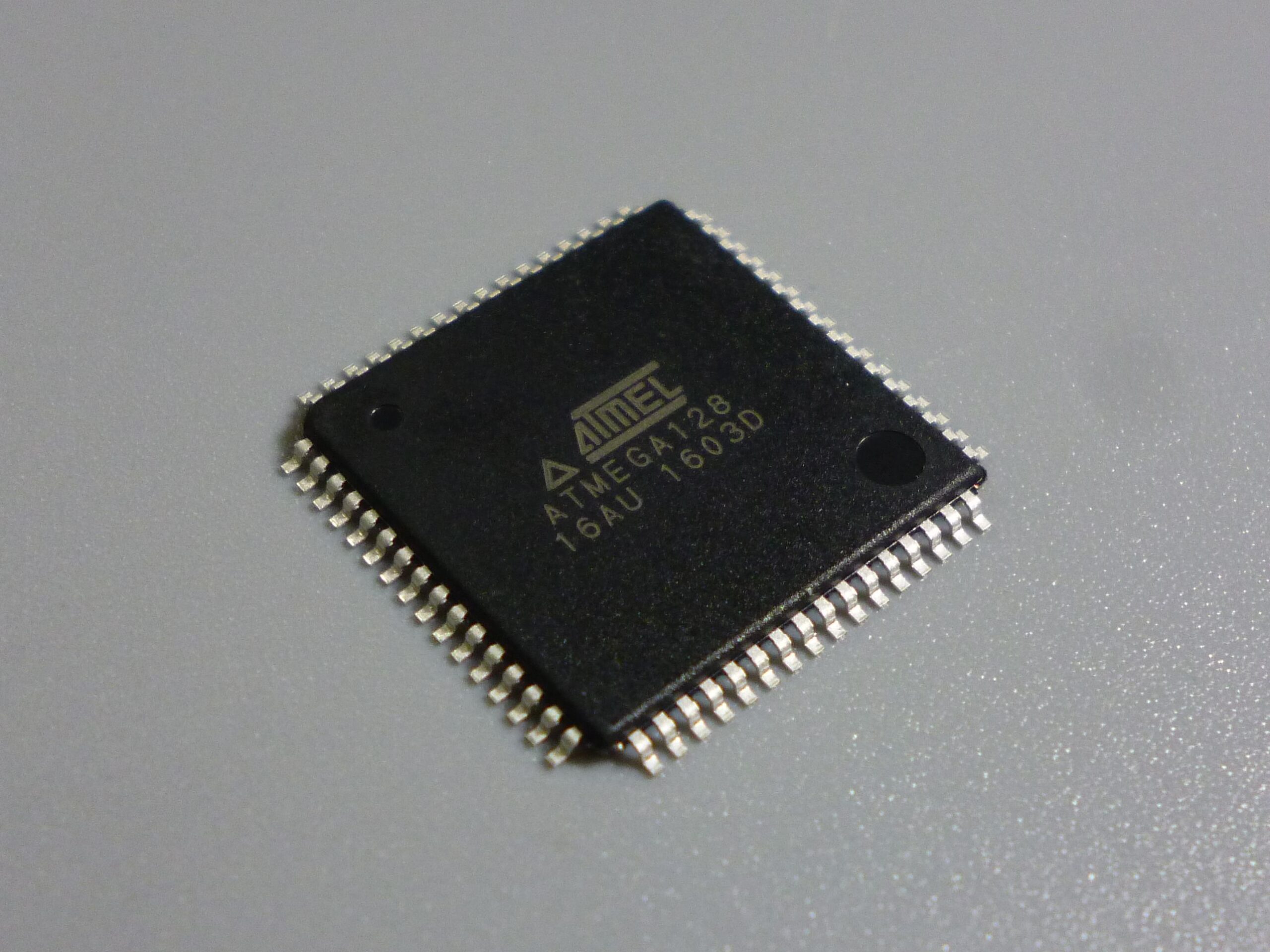
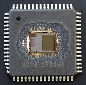
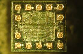
 Break Microcontroller ATmega128 Heximal
Break Microcontroller ATmega128 Heximal
We can Break Microcontroller ATmega128 heximal, please view the Microcontroller Atmega128 features for your reference:
Features
· High-performance, Low-power AVR 8-bit Microcontroller
· Advanced RISC Architecture
– 133 Powerful Instructions – Most Single Clock Cycle Execution
– 32 x 8 General Purpose Working Registers + Peripheral Control Registers
– Fully Static Operation
– Up to 16 MIPS Throughput at 16 MHz
– On-chip 2-cycle Multiplier
Nonvolatile Program and Data Memories
– 128K Bytes of In-System Reprogrammable Flash
knacken Sie das Atmel ATMEGA128 gesperrte Mikrocontroller-Manipulationswiderstandssystem und kopieren Sie die gesperrte ATMEGA128-Embedded Heximal-Datei des Mikroprozessors auf die neue MCU-Einhei
Endurance: 1,000 Write/Erase Cycles
– Optional Boot Code Section with Independent Lock Bits
In-System Programming by On-chip Boot Program
True Read-While-Write Operation
– 4K Bytes EEPROM
Endurance: 100,000 Write/Erase Cycles
– 4K Bytes Internal SRAM
– Up to 64K Bytes Optional External Memory Space
– Programming Lock for Software Security
– SPI Interface for In-System Programming
JTAG (IEEE std. 1149.1 Compliant) Interface
– Boundary-scan Capabilities According to the JTAG Standard
– Extensive On-chip Debug Support
– Programming of Flash, EEPROM, Fuses and Lock Bits through the JTAG Interface
Peripheral Features
– Two 8-bit Timer/Counters with Separate Prescalers and Compare Modes
– Two Expanded 16-bit Timer/Counters with Separate Prescaler, Compare Mode and Capture Mode
– Real Time Counter with Separate Oscillator
– Two 8-bit PWM Channels
– 6 PWM Channels with Programmable Resolution from 1 to 16 Bits
– 8-channel, 10-bit ADC
8 Single-ended Channels
7 Differential Channels
2 Differential Channels with Programmable Gain (1x, 10x, 200x)
– Byte-oriented 2-wire Serial Interface
– Dual Programmable Serial USARTs
– Master/Slave SPI Serial Interface
– Programmable Watchdog Timer with On-chip Oscillator
– On-chip Analog Comparator
Special Microcontroller Features
– Power-on Reset and Programmable Brown-out Detection
– Internal Calibrated RC Oscillator
– External and Internal Interrupt Sources
الكراك atmel ATMEGA128 نظام مقاومة عبث متحكم مقفل ونسخ معالج دقيق ATMEGA128 مضمن إلى وحدة MCU جديدة
– Six Sleep Modes: Idle, ADC Noise Reduction, Power-save, Power-down, Standby and Extended Standby
– Software Selectable Clock Frequency
– ATmega103 Compatibility Mode Selected by a Fuse
– Global Pull-up Disable
I/O and Packages
– 53 Programmable I/O Lines
– 64-lead TQFP
Operating Voltages
– 2.7 – 5.5V (ATmega128L)
– 4.5 – 5.5V (ATmega128)
Speed Grades
– 0 – 8 MHz (ATmega128L)
– 0 – 16 MHz (ATmega128)
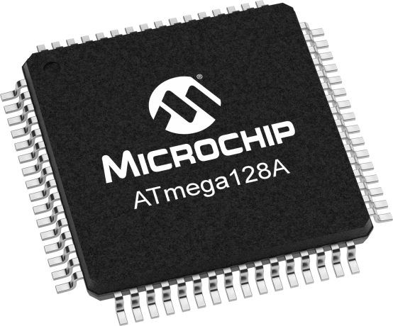
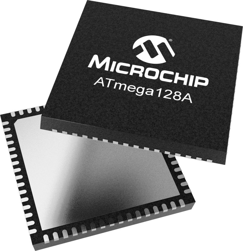
Break MCU ATmega128A Flash

Break MCU ATmega128A Flash
We can Break MCU Atmega128a Flash, please view the MCU Atmega128a features below for your reference:
Features
· High-performance, Low-power AVR 8-bit MCU
· Advanced RISC Architecture
– 133 Powerful Instructions – Most Single Clock Cycle Execution
– 32 x 8 General Purpose Working Registers + Peripheral Control Registers
– Fully Static Operation
– Up to 16 MIPS Throughput at 16 MHz
– On-chip 2-cycle Multiplier
High Endurance Non-volatile Memory segments
– 128K Bytes of In-System Self-programmable Flash program memory
– 4K Bytes EEPROM
– 4K Bytes Internal SRAM
– Write/Erase cycles: 10,000 Flash/100,000 EEPROM
– Data retention: 20 years at 85°C/100 years at 25°C(1)
– Optional Boot Code Section with Independent Lock Bits
In-System Programming by On-chip Boot Program
ロックされたマイクロコントローラーatmega128aセキュリティヒューズビットを解除し、atmega128aで保護されたマイクロプロセッサーから組み込みヘキシマルを読み取り、元のバイナリプログラムを新しいatmega128aMCUユニットに複製します。
True Read-While-Write Operation to facilitate MCU Cracking
– Up to 64K Bytes Optional External Memory Space
– Programming Lock for Software Security
– SPI Interface for In-System Programming
JTAG (IEEE std. 1149.1 Compliant) Interface
– Boundary-scan Capabilities According to the JTAG Standard
– Extensive On-chip Debug Support
– Programming of Flash, EEPROM, Fuses and Lock Bits through the JTAG Interface
Peripheral Features
– Two 8-bit Timer/Counters with Separate Prescalers and Compare Modes
– Two Expanded 16-bit Timer/Counters with Separate Prescaler, Compare Mode and
Capture Mode
잠긴 마이크로컨트롤러 atmega128a 보안 퓨즈 비트를 끊고 atmega128a 보안 마이크로프로세서에서 임베디드 16진수 판독, 원본 바이너리 프로그램을 새로운 atmega128a MCU 장치로 복제,
– Real Time Counter with Separate Oscillator
– Two 8-bit PWM Channels
– 6 PWM Channels with Programmable Resolution from 2 to 16 Bits
– Output Compare Modulator
– 8-channel, 10-bit ADC
8 Single-ended Channels
7 Differential Channels
2 Differential Channels with Programmable Gain at 1x, 10x, or 200x
– Byte-oriented Two-wire Serial Interface
– Dual Programmable Serial USARTs
– Master/Slave SPI Serial Interface
– Programmable Watchdog Timer with On-chip Oscillator
– On-chip Analog Comparator
Special MCU Features
– Power-on Reset and Programmable Brown-out Detection
– Internal Calibrated RC Oscillator
– External and Internal Interrupt Sources
– Six Sleep Modes: Idle, ADC Noise Reduction, Power-save, Power-down, Standby, and Extended Standby
– Software Selectable Clock Frequency
– ATmega103 Compatibility Mode Selected by a Fuse
– Global Pull-up Disable
I/O and Packages
– 53 Programmable I/O Lines
– 64-lead TQFP and 64-pad QFN/MLF
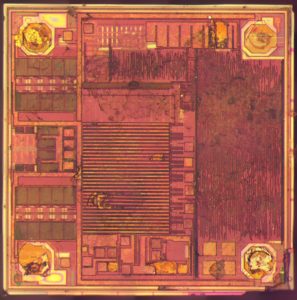
Break IC MC9S12XDG128 Heximal
Break IC MC9S12XDG128 Heximal
We can Break IC MC9S12XDG128 Heximal, please view below IC MC9S12XDG128 features for your reference:
Introduction
Targeted at automotive multiplexing applications, the MC9S12XD Family will deliver 32-bit performance with all the advantages and efficiencies of a 16-bit MCU. The S12X is designed to retain the low cost, low power consumption, excellent EMC performance and code-size efficiency advantages enjoyed by users of Freescale’s previous 16-bit MC9S12 MCU family.
Based around an enhanced S12 core, the MC9S12XD Family will deliver two to five times the performance of a 25 MHz S12 whilst retaining a high degree of pin and code compatibility with the original S12D – family.
The MC9S12XD Family features the performance boosting XGATE co-processor. The XGATE, which is programmable in “C” language, has an instruction set which is optimized for data movement, logic and bit manipulation instructions. It runs at twice the bus frequency of the S12X and off-loads the CPU by providing high speed data transfer (and data processing) between any peripheral module, RAM and I/O ports before Break IC. This is particularly useful in applications such as automotive gateways where there are multiple busses carrying heavy data traffic which would otherwise exert a heavy interrupt/processing load on the CPU.
The MC9S12XD Family will feature an enhanced MSCAN module which, when used in conjunction with XGATE, delivers FullCAN performance with virtually unlimited number of mailboxes and retains backwards compatibility with the MSCAN module featured on previous S12 products.
Memory options will range from 64 Kbytes to 512 Kbytes of Freescale’s industry-leading, full automotive spec SG-Flash with additional integrated EEPROM.
In addition to the rich S12 peripheral set, the MC9S12XD Family will feature more RAM, extra A/D channels, new timer features and additional LIN-compatible SCI ports compared with the original S12 D Family. The MC9S12XD Family also features a new flexible interrupt handler which allows multilevel nested interrupts.
The MC9S12XD Family has full 16-bit data paths throughout. The non-multiplexed expanded bus interface available on the 144-pin versions allows an easy interface to external memories. The inclusion of a PLL circuit allows power consumption and performance to be adjusted to suit operational requirements. System power consumption is further improved with the new “fast exit from STOP mode” feature and an ultra low power wakeup timer.
In addition to the I/O ports available in each module, up to 25 further I/O ports are available with interrupt capability allowing wakeup from STOP or WAIT mode.
The MC9S12XD Family will be available in 144-pin LQFP (with optional external bus), 112-pin, and 80-pin options.
Break AVR ATmega64A Binary
Break AVR ATmega64A Binary
We can Break AVR ATMEGA64A Binary, please view below AVR ATMEGA64A features for your reference:
· High-performance, Low-power AVR® 8-bit Microcontroller
· Advanced RISC Architecture
– 130 Powerful Instructions – Most Single Clock Cycle Execution
– 32 x 8 General Purpose Working Registers + Peripheral Control Registers
– Fully Static Operation
– Up to 16 MIPS Throughput at 16 MHz
– On-chip 2-cycle Multiplier
High Endurance Non-volatile Memory segments
– 64K Bytes of In-System Reprogrammable Flash program memory
– 2K Bytes EEPROM
– 4K Bytes Internal SRAM
– Write/Erase Cycles: 10,000 Flash/100,000 EEPROM
– Data retention: 20 years at 85°C/100 years at 25°C(1)
– Optional Boot Code Section with Independent Lock Bits
· In-System Programming by On-chip Boot Program
· True Read-While-Write Operation
– Up to 64K Bytes Optional External Memory Space
– Programming Lock for Software Security
– SPI Interface for In-System Programming
JTAG (IEEE std. 1149.1 Compliant) Interface
– Boundary-scan Capabilities According to the JTAG Standard
– Extensive On-chip Debug Support
– Programming of Flash, EEPROM, Fuses, and Lock Bits through the JTAG Interface
Peripheral Features
– Two 8-bit Timer/Counters with Separate Prescalers and Compare Modes
– Two Expanded 16-bit Timer/Counters with Separate Prescaler, Compare Mode, and Capture Mode
– Real Time Counter with Separate Oscillator
– Two 8-bit PWM Channels
– 6 PWM Channels with Programmable Resolution from 1 to 16 Bits
– 8-channel, 10-bit ADC
· 8 Single-ended Channels
· 7 Differential Channels
· 2 Differential Channels with Programmable Gain (1x, 10x, 200x)
– Byte-oriented Two-wire Serial Interface
– Dual Programmable Serial USARTs
– Master/Slave SPI Serial Interface
– Programmable Watchdog Timer with On-chip Oscillator
– On-chip Analog Comparator
Special Microcontroller Features
– Power-on Reset and Programmable Brown-out Detection
– Internal Calibrated RC Oscillator
– External and Internal Interrupt Sources when Break AVR
– Six Sleep Modes: Idle, ADC Noise Reduction, Power-save, Power-down, Standby and Extended Standby
– Software Selectable Clock Frequency
– ATmega103 Compatibility Mode Selected by a Fuse
– Global Pull-up Disable I/O and Packages
– 53 Programmable I/O Lines
– 64-lead TQFP and 64-pad QFN/MLF Operating Voltages
– 2.7 – 5.5V for ATmega64A Speed Grades
Recover MCU ATmega8 Flash
We can Recover MCU ATMEGA8 Flash, please see below MCU ATMEGA8 features for your reference:
Features
· High-performance, Low-power AVR® 8-bit Microcontroller
· Advanced RISC Architecture
– 130 Powerful Instructions – Most Single-clock Cycle Execution
– 32 x 8 General Purpose Working Registers
– Fully Static Operation
– Up to 16 MIPS Throughput at 16 MHz
– On-chip 2-cycle Multiplier
Nonvolatile Program and Data Memories
– 8K Bytes of In-System Self-Programmable Flash
Endurance: 10,000 Write/Erase Cycles
– Optional Boot Code Section with Independent Lock Bits
In-System Programming by On-chip Boot Program
True Read-While-Write Operation
– 512 Bytes EEPROM
Endurance: 100,000 Write/Erase Cycles
– 1K Byte Internal SRAM
– Programming Lock for Software Security
Peripheral Features
– Two 8-bit Timer/Counters with Separate Prescaler, one Compare Mode
– One 16-bit Timer/Counter with Separate Prescaler, Compare Mode, and Capture
Mode
– Real Time Counter with Separate Oscillator
– Three PWM Channels
– 8-channel ADC in TQFP and QFN/MLF package
Eight Channels 10-bit Accuracy
– 6-channel ADC in PDIP package
Eight Channels 10-bit Accuracy
– Byte-oriented Two-wire Serial Interface
– Programmable Serial USART
– Master/Slave SPI Serial Interface
– Programmable Watchdog Timer with Separate On-chip Oscillator
– On-chip Analog Comparator
Special Microcontroller Features
– Power-on Reset and Programmable Brown-out Detection
– Internal Calibrated RC Oscillator
– External and Internal Interrupt Sources
– Five Sleep Modes: Idle, ADC Noise Reduction, Power-save, Power-down, and Standby
I/O and Packages
– 23 Programmable I/O Lines
– 28-lead PDIP, 32-lead TQFP, and 32-pad QFN/MLF
Operating Voltages
– 2.7 – 5.5V (ATmega8L)
– 4.5 – 5.5V (ATmega8)
Speed Grades
– 0 – 8 MHz (ATmega8L)
– 0 – 16 MHz (ATmega8)
Power Consumption at 4 Mhz, 3V, 25°C
Recover Microcontroller STM32F105RCT6TR Binary

Recover Microcontroller STM32F105RCT6TR Binary
We can Recover Microcontroller STM32F105RCT6TR Binary, please view below Microcontroller STM32F105RCT6TR features for your reference:
Features
Core: ARM 32-bit Cortex™-M3 CPU
– 72 MHz maximum frequency, 1.25 DMIPS/MHz (Dhrystone 2.1) performance at 0 wait state memory
LQFP100 14 × 14 mm
LQFP64 10 × 10 mm
access
– Single-cycle multiplication and hardware division
Memories
– 64 to 256 Kbytes of Flash memory
– up to 64 Kbytes of general-purpose SRAM Clock, reset and supply management
– 2.0 to 3.6 V application supply and I/Os
– POR, PDR, and programmable voltage detector (PVD)
– 3-to-25 MHz crystal oscillator
– Internal 8 MHz factory-trimmed RC
– Internal 40 kHz RC with calibration
– 32 kHz oscillator for RTC with calibration Low power
– Sleep, Stop and Standby modes
– VBAT supply for RTC and backup registers
2 × 12-bit, 1 µs A/D converters (16 channels)
– Conversion range: 0 to 3.6 V
– Sample and hold capability
– Temperature sensor
– up to 2 MSPS in interleaved mode 2 × 12-bit D/A converters DMA: 12-channel DMA controller
– Supported peripherals: timers, ADCs, DAC, I2Ss, SPIs, I2Cs and USARTs
Up to 10 timers with pinout remap capability
– Up to four 16-bit timers, each with up to 4 IC/OC/PWM or pulse counter and quadrature (incremental) encoder input
– 1 × 16-bit motor control PWM timer with dead-time generation and emergency stop
– 2 × watchdog timers (Independent and Window)
– SysTick timer: a 24-bit downcounter
– 2 × 16-bit basic timers to drive the DAC Up to 14 communication interfaces with pinout remap capability
– Up to 2 × I2C interfaces (SMBus/PMBus)
– Up to 5 USARTs (ISO 7816 interface, LIN, IrDA capability, modem control)
– Up to 3 SPIs (18 Mbit/s), 2 with a multiplexed I2S interface that offers audio class accuracy via advanced PLL schemes
– 2 × CAN interfaces (2.0B Active) with 512 bytes of dedicated SRAM
– USB 2.0 full-speed device/host/OTG controller with on-chip PHY that supports HNP/SRP/ID with 1.25 Kbytes of dedicated SRAM
– 10/100 Ethernet MAC with dedicated DMA and SRAM (4 Kbytes): IEEE1588 hardware support, MII/RMII available on all packages
Table 1.
Device summary
– Serial wire debug (SWD) & JTAG interfaces
Reference
Part number
– Cortex-M3 Embedded Trace Macrocell™
Up to 80 fast I/O ports
– 51/80 I/Os, all mappable on 16 external interrupt vectors and almost all 5 V-tolerant CRC calculation unit, 96-bit unique ID
STM32F105xx
STM32F107xx
STM32F105R8, STM32F105V8
STM32F105RB, STM32F105VB
STM32F105RC, STM32F105VC
STM32F107RB, STM32F107VB
STM32F107RC, STM32F107VC
Recover Chip EPM7064AETC100-4N Software
Recover Chip EPM7064AETC100-4N Software
We can recover Chip EPM7064AETC100-4N software, please view below Chip EPM7064AETC100-4N features for your reference:
High-performance 3.3-V EEPROM-based programmable logic devices (PLDs) built on second-generation Multiple Array MatriX
3.3-V in-system programmability (ISP) through the built-in IEEE Std. 1149.1 Joint Test Action Group (JTAG) interface with advanced pin-locking capability
– MAX 7000AE device in-system programmability (ISP) circuitry compliant with IEEE Std. 1532
– EPM7128A and EPM7256A device ISP circuitry compatible with IEEE Std. 1532
Built-in boundary-scan test (BST) circuitry compliant with IEEE Std. 1149.1
Supports JEDEC Jam Standard Test and Programming Language (STAPL) JESD-71
Enhanced ISP features
– Enhanced ISP algorithm for faster programming (excluding EPM7128A and EPM7256A devices)
– ISP_Done bit to ensure complete programming (excluding EPM7128A and EPM7256A devices)
– Pull-up resistor on I/O pins during in-system
– Pin-compatible with the popular
4.5-ns pin-to-pin logic delays with counter frequencies of up to 227.3 MHz
MultiVoltTM I/O interface enables device core to run at 3.3 V, while I/O pins are compatible with 5.0-V, 3.3-V, and 2.5-V logic levels Pin counts ranging from 44 to 256 in a variety of thin quad flat pack (TQFP), plastic quad flat pack (PQFP), ball-grid array (BGA), space-saving FineLine BGATM, and plastic J-lead chip carrier (PLCC) packages.
Supports hot-socketing in MAX 7000AE devices
Programmable interconnect array (PIA) continuous routing structure for fast, predictable performance
PCI-compatible
Bus-friendly architecture, including programmable slew-rate control
Open-drain output option
Programmable macrocell registers with individual clear, preset, clock, and clock enable controls
Programmable power-up states for macrocell registers in MAX 7000AE devices
Programmable power-saving mode for 50% or greater power reduction in each macrocell
Configurable expander product-term distribution, allowing up to 32 product terms per macrocell
Programmable security bit for protection of proprietary designs 6 to 10 pin- or logic-driven output enable signals
Two global clock signals with optional inversion
Enhanced interconnect resources for improved routability
Fast input setup times provided by a dedicated path from I/O pin to macrocell registers
Programmable output slew-rate control
Programmable ground pins
Software design support and automatic place-and-route provided by Altera’s development systems for Windows-based PCs and Sun SPARCstation, and HP 9000 Series 700/800 workstations Additional design entry and simulation support provided by EDIF 2 0 0 and 3 0 0 netlist files, library of parameterized modules (LPM), Verilog HDL, VHDL, and other interfaces to popular EDA tools from manufacturers such as Cadence, Exemplar Logic, Mentor Graphics, OrCAD, Synopsys, Synplicity, and VeriBest
Programming support with Altera’s Master Programming Unit (MPU), MasterBlasterTM serial/universal serial bus (USB) communications cable, ByteBlasterMVTM parallel port download cable, and BitBlasterTM serial download cable, as well as programming hardware from third-party manufacturers and any JamTM STAPL File (.jam), Jam Byte-Code File (.jbc), or Serial Vector Format File- (.svf) capable in-circuit tester.
Recover IC ATmega64L Binary
Recover IC ATmega64L Binary
We can Recover IC ATMEGA64L Binary, please view below IC ATMEGA64L features for your reference:
· High-performance, Low-power Atmel® AVR® 8-bit Microcontroller
· Advanced RISC Architecture
– 130 Powerful Instructions – Most Single Clock Cycle Execution
– 32 x 8 General Purpose Working Registers + Peripheral Control Registers
– Fully Static Operation
– Up to 16 MIPS Throughput at 16 MHz
– On-chip 2-cycle Multiplier
High Endurance Non-volatile Memory segments
– 64 Kbytes of In-System Reprogrammable Flash program memory
– 2 Kbytes EEPROM
– 4 Kbytes Internal SRAM
– Write/Erase Cycles: 10,000 Flash/100,000 EEPROM
– Data retention: 20 years at 85°C/100 years at 25°C(1)
– Optional Boot Code Section with Independent Lock Bits
In-System Programming by On-chip Boot Program
True Read-While-Write Operation
– Up to 64 Kbytes Optional External Memory Space
– Programming Lock for Software Security
– SPI Interface for In-System Programming
JTAG (IEEE std. 1149.1 Compliant) Interface
– Boundary-scan Capabilities According to the JTAG Standard
– Extensive On-chip Debug Support
– Programming of Flash, EEPROM, Fuses, and Lock Bits through the JTAG Interface
Peripheral Features
– Two 8-bit Timer/Counters with Separate Prescalers and Compare Modes
– Two Expanded 16-bit Timer/Counters with Separate Prescaler, Compare Mode, and Capture Mode
– Real Time Counter with Separate Oscillator
– Two 8-bit PWM Channels
– 6 PWM Channels with Programmable Resolution from 1 to 16 Bits
– 8-channel, 10-bit ADC
8 Single-ended Channels
7 Differential Channels
2 Differential Channels with Programmable Gain (1x, 10x, 200x)
– Byte-oriented Two-wire Serial Interface
– Dual Programmable Serial USARTs
– Master/Slave SPI Serial Interface
– Programmable Watchdog Timer with On-chip Oscillator
– On-chip Analog Comparator
Special Microcontroller Features
– Power-on Reset and Programmable Brown-out Detection
– Internal Calibrated RC Oscillator
– External and Internal Interrupt Sources
– Six Sleep Modes: Idle, ADC Noise Reduction, Power-save, Power-down, Standby
and Extended Standby
– Software Selectable Clock Frequency
– ATmega103 Compatibility Mode Selected by a Fuse
– Global Pull-up Disable
I/O and Packages
– 53 Programmable I/O Lines
– 64-lead TQFP and 64-pad QFN/MLF
Operating Voltages
– 2.7V – 5.5V for ATmega64L
– 4.5V – 5.5V for ATmega64
Speed Grades
– 0 – 8 MHz for ATmega64L
– 0 – 16 MHz for ATmega64
Break IC ATmega169P Code
The calibrated internal RC Oscillator provides a fixed 8.0 MHz clock. The frequency is nominal value at 3V and 25°C. If 8 MHz frequency exceeds the specification of the device (depends on VCC), the CKDIV8 Fuse must be programmed in order to divide the internal frequency by 8 during start-up to facilitate Break IC ATmega169P Code.
Break IC ATmega169P Code
The device is shipped with the CKDIV8 Fuse programmed. See “System Clock Prescaler” on page 29. for more details. This clock may be selected as the system clock by programming the CKSEL Fuses as shown in Table 8. If selected, it will operate with no external components. During reset, hardware loads the calibration byte into the OSCCAL Register and thereby automatically calibrates the RC Oscillator.
At 3V and 25°C, this calibration gives a frequency within ± 10% of the nominal frequency. Using calibration methods as described in application notes available at www.atmel.com/avr it is possible to achieve ± 2% accuracy at any given VCC and Temperature. When this Oscillator is used as the IC clock, the Watchdog Oscillator will still be used for the Watchdog Timer and for the Reset Time-out.
For more information on the pre-programmed calibration value, see the section “Calibration Byte” on page 269. When this Oscillator is selected, start-up times are determined by the SUT Fuses as shown in Table 9. Selecting internal RC Oscillator allows the XTAL1/TOSC1 and XTAL2/TOSC2 pins to be used as timer oscillator pins.
Writing the calibration byte to this address will trim the internal Oscillator to remove process variations from the Oscillator frequency. This is done automatically during IC Reset. When OSCCAL is zero, the lowest available frequency is chosen in the process of Break IC ATmega169P Code. Writing nonzero values to this register will increase the frequency of the internal Oscillator.
Writing 0x7F to the register gives the highest available frequency. The calibrated Oscillator is used to time EEPROM and Flash access. If EEPROM or Flash is written, do not calibrate to more than 10% above the nominal frequency. Otherwise, the EEPROM or Flash write may fail. Note that the Oscillator is intended for calibration to 8.0 MHz. Tuning to other values is not guaranteed, as indicated in Table 10.
When applying an external clock, it is required to avoid sudden changes in the applied clock frequency to ensure stable operation of the MCU. A variation in frequency of more than 2% from one clock cycle to the next can lead to unpredictable behavior. It is required to ensure that the MCU is kept in Reset during such changes in the clock frequency.
Note that the System Clock Prescaler can be used to implement run-time changes of the internal clock frequency while still ensuring stable operation. Refer to “System Clock Prescaler” on page 29 for details. When the CKOUT Fuse is programmed, the system Clock will be output on CLKO. This mode is suitable when IC clock is used to drive other circuits on the system.
The clock will be output also during reset and the normal operation of I/O pin will be overridden when the fuse is programmed. Any clock source, including internal RC Oscillator, can be selected when CLKO serves as clock output. If the System Clock Prescaler is used, it is the divided system clock that is output when the CKOUT Fuse is programmed.
Copy Chip ATmega64L Eeprom
Copy Chip ATmega64L Eeprom
We can Copy Chip ATmega64L Eeprom, please view below chip features for your reference:
· High-performance, Low-power Atmel® CHIP® 8-bit Microcontroller
· Advanced RISC Architecture
– 130 Powerful Instructions – Most Single Clock Cycle Execution
– 32 x 8 General Purpose Working Registers + Peripheral Control Registers
– Fully Static Operation
– Up to 16 MIPS Throughput at 16 MHz
– On-chip 2-cycle Multiplier
High Endurance Non-volatile Memory segments
– 64 Kbytes of In-System Reprogrammable Flash program memory
– 2 Kbytes EEPROM
– 4 Kbytes Internal SRAM
– Write/Erase Cycles: 10,000 Flash/100,000 EEPROM
– Data retention: 20 years at 85°C/100 years at 25°C(1)
– Optional Boot Code Section with Independent Lock Bits
In-System Programming by On-chip Boot Program
True Read-While-Write Operation
– Up to 64 Kbytes Optional External Memory Space
– Programming Lock for Software Security
– SPI Interface for In-System Programming
JTAG (IEEE std. 1149.1 Compliant) Interface
– Boundary-scan Capabilities According to the JTAG Standard
– Extensive On-chip Debug Support
– Programming of Flash, EEPROM, Fuses, and Lock Bits through the JTAG Interface
Peripheral Features
– Two 8-bit Timer/Counters with Separate Prescalers and Compare Modes
– Two Expanded 16-bit Timer/Counters with Separate Prescaler, Compare Mode, and Capture Mode
– Real Time Counter with Separate Oscillator
– Two 8-bit PWM Channels
– 6 PWM Channels with Programmable Resolution from 1 to 16 Bits
– 8-channel, 10-bit ADC
8 Single-ended Channels
7 Differential Channels
2 Differential Channels with Programmable Gain (1x, 10x, 200x)
– Byte-oriented Two-wire Serial Interface
– Dual Programmable Serial USARTs
– Master/Slave SPI Serial Interface
– Programmable Watchdog Timer with On-chip Oscillator
– On-chip Analog Comparator
Special Microcontroller Features
– Power-on Reset and Programmable Brown-out Detection
– Internal Calibrated RC Oscillator
– External and Internal Interrupt Sources
– Six Sleep Modes: Idle, ADC Noise Reduction, Power-save, Power-down, Standby
and Extended Standby
– Software Selectable Clock Frequency
– ATmega103 Compatibility Mode Selected by a Fuse
– Global Pull-up Disable
I/O and Packages
– 53 Programmable I/O Lines
– 64-lead TQFP and 64-pad QFN/MLF
Operating Voltages
– 2.7V – 5.5V for ATmega64L
– 4.5V – 5.5V for ATmega64
Speed Grades
– 0 – 8 MHz for ATmega64L
– 0 – 16 MHz for ATmega64