Archive for July, 2014
 Copy Microcontroller PIC16C76 Heximal
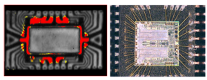
Copy Microcontroller PIC16C76 Heximal
We can Copy Microcontroller PIC16C76 Heximal, please view the Microcontroller PIC16C76 features for your reference:
Any instruction which writes, operates internally as a read followed by a write operation. The BCF and BSF instructions, for example, read the register into the CPU, execute the bit operation and write the result back to the register.
Caution must be used when these instructions are applied to a port with both inputs and outputs defined. For example, a BSF operation on bit5 of PORTB will cause all eight bits of PORTB to be read into the CPU.
Then the BSF operation takes place on bit5 and PORTB is written to the output latches. If another bit of PORTB is used as a bi-directional I/O pin (e.g., bit0) and it is defined as an input at this time, the input signal present on the pin itself would be read into the CPU and rewritten to the data latch of this particular pin, overwriting the previous content.
As long as the pin stays in the input mode, no problem occurs. However, if bit0 is switched to an output, the content of the data latch may now be unknown.
Reading the port register, reads the values of the port pins. Writing to the port register writes the value to the port latch. When using read-modify-write instructions (ex.BCF, BSF, etc.) on a port, the value of the port pins is read, the desired operation is done to this value, and this value is then written to the port latch.
Example 5-4 shows the effect of two sequential read-modify-write instructions on an I/O port. A pin actively outputting a Low or High should not be driven from external devices at the same time in order to change the level on this pin (“wired-or”, “wired-and”). The resulting high output currents may damage the chip.
The actual write to an I/O port happens at the end of an instruction cycle, whereas for reading, the data must be valid at the beginning of the instruction cycle (Figure 5-10). Therefore, care must be exercised if a write followed by a read operation is carried out on the same I/ O port.
The sequence of instructions should be such to allow the pin voltage to stabilize (load dependent) before the next instruction which causes that file to be read into the CPU is executed. Otherwise, the previous state of that pin may be read into the CPU rather than the new state in the process of Copy Microcontroller PIC16C76 Heximal. When in doubt, it is better to separate these instructions with a NOP or another instruction not accessing this I/O port.
It can directly interface to an 8-bit microprocessor data bus. The external microprocessor can read or write the PORTD latch as an 8-bi t latch. Setting bit PSPMODE enables port pin RE0/RD/AN5 to be the RD input, RE1/WR/AN6 to be the WR input and RE2/CS/AN7 to be the CS (chip select) input to Crack MCU. For this functionality, the corresponding data direction bits of the TRISE register (TRISE<2:0>) must be configured as inputs (set) and the A/D port configuration bits PCFG2:PCFG0 (ADCON1<2:0>) must be set, which will configure pins RE2:RE0 as digital I/O.
Copy IC PIC16F84 Code
Copy IC PIC16F84 Code
All PICmicro™ microcontrollers employ an advanced RISC architecture. PIC16F8X devices have enhanced core features, eight-level deep stack, and multiple internal and external interrupt sources. The separate instruction and data buses of the Harvard architecture allow a 14-bit wide instruction word with a separate 8-bit wide data bus which can be used for Copy IC PIC16F84 Code. The two stage instruction pipeline allows all instructions to execute in a single cycle, except for program branches (which require two cycles). A total of 35 instructions (reduced instruction set) are available. Additionally, a large register set is used to achieve a very high performance level.
PIC16F8X microcontrollers typically achieve a 2:1 code compression and up to a 4:1 speed improvement (at 20 MHz) over other 8-bit microcontrollers in their class.
The PIC16F8X has up to 68 bytes of RAM, 64 bytes of Data EEPROM memory, and 13 I/O pins. A timer/counter is also available.
The PIC16CXX family has special features to reduce external components, thus reducing cost, enhancing system reliability and reducing power consumption.
There are four oscillator options, of which the single pin RC oscillator provides a low-cost solution, the LP oscillator minimizes power consumption, XT is a standard crystal, and the HS is for High Speed crystals.
The SLEEP (power-down) mode offers power saving. The user can wake the chip from sleep through several external and internal interrupts and resets. A highly reliable Watchdog Timer with its own on-chip RC oscillator provides protection against software lock-up. The devices with Flash program memory allow the same device package to be used for prototyping and production.
In-circuit reprogrammability allows the code to be updated without the device being removed from the end application. This is useful in the development of many applications where the device may not be easily accessible to Copy IC PIC16F84 Code, but the prototypes may require code updates. This is also useful for remote applications where the code may need to be updated (such as rate information).
The PIC16F8X fits perfectly in applications ranging from high speed automotive and appliance motor control to low-power remote sensors, electronic locks, security devices and smart cards. The Flash/EEPROM technology makes customization of application programs (transmitter codes, motor speeds, receiver frequencies, security codes, etc.) extremely fast and convenient.
The small footprint packages make this microcontroller series perfect for all applications with space limitations. Low-cost, low-power, high performance, ease-of-use and I/O flexibility make the PIC16F8X very versatile even in areas where no microcontroller use has been considered before when Crack MCU (e.g., timer functions; serial communication; capture, compare and PWM functions; and co-processor applications).
The serial in-system programming feature (via two pins) offers flexibility of customizing the product after complete assembly and testing. This feature can be used to serialize a product, store calibration data, or program the device with the current firmware before shipping.
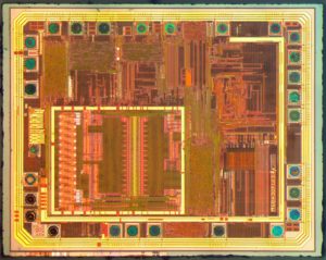
Copy MCU PIC16C554A Eeprom
Copy MCU PIC16C554A Eeprom
The PIC16C55X(A) are 18 and 20-Pin EPROM-based members of the versatile PIC16CXX family of low-cost, high-performance, CMOS, fully-static, 8-bit microcontrollers which is the reason for Copy MCU PIC16C554A Eeprom.
All PICmicro™ microcontrollers employ an advanced RISC architecture. The PIC16C55X(A) have enhanced core features, eight-level deep stack, and multiple internal and external interrupt sources. The separate instruction and data buses of the Harvard architecture allow a 14-bit wide instruction word with the separate 8-bit wide data.
The two-stage instruction pipeline allows all instructions to execute in a single-cycle, except for program branches (which require two cycles). A total of 35 instructions (reduced instruction set) are available. Additionally, a large register set gives some of the architectural innovations used to achieve a very high performance.
PIC16C55X(A) microcontrollers typically achieve a 2:1 code compression and a 4:1 speed improvement over other 8-bit microcontrollers in their class.
The PIC16C554(A) and PIC16C556A have 80 bytes of RAM. The PIC16C558(A) has 128 bytes of RAM. Each device has 13 I/O pins and an 8-bit timer/counter with an 8-bit programmable prescaler.
PIC16C55X(A) devices have special features to reduce external components, thus reducing cost, enhancing system reliability and reducing power consumption in the process of Copy MCU PIC16C554A Eeprom.
There are four oscillator options, of which the single pin RC oscillator provides a low-cost solution, the LP oscillator minimizes power consumption, XT is a standard crystal, and the HS is for High Speed crystals. The SLEEP (power-down) mode offers power saving.
The user can wake up the MCU from SLEEP through several external and internal interrupts and reset.A highly reliable Watchdog Timer with its own on-MCU RC oscillator provides protection against software lock- up. A UV-erasable CERDIP-packaged version is ideal for code development while the cost-effective One-Time Programmable (OTP) version is suitable for production in any volume.
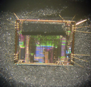
Attack Chip PIC16C622A Software

Attack Chip PIC16C622A Software
The high performance of the PIC16C62X family can be attributed to a number of architectural features commonly found in RISC microprocessors which is critical feature for Attack Chip PIC16C622A Software. To begin with, the PIC16C62X uses a Harvard architecture, in which, program and data are accessed from separate memories using separate busses. This improves bandwidth over traditional von Neumann architecture where program and data are fetched from the same memory. Separating program and data memory further allows instructions to be sized differently than 8-bit wide data word. Instruction opcodes are 14-bits wide making it possible to have all single word instructions.
A 14-bit wide program memory access bus fetches a 14-bit instruction in a single cycle. A two-stage pipeline overlaps fetch and execution of instructions.
Consequently, all instructions (35) execute in a single-cycle (200 ns @ 20 MHz) except for program branches. The PIC16C620A and PIC16CR620A address 512 x 14 on-chip program memory. The PIC16C621(A) addresses 1K x 14 program memory. The PIC16C622(A) addresses 2K x 14 program memory. All program memory is internal.
The PIC16C62X can directly or indirectly address its register files or data memory. All special function registers including the program counter are mapped in the data memory. The PIC16C62X have an orthogonal (symmetrical) instruction set that makes it possible to carry out any operation on any register using any addressing mode in order to Attack Chip PIC16C622A Software. This symmetrical nature and lack of ‘special optimal situations’ make programming with the PIC16C62X simple yet efficient. In addition, the learning curve is reduced significantly.
The PIC16C62X devices contain an 8-bit ALU and working register. The ALU is a general purpose arithmetic unit. It performs arithmetic and Boolean functions between data in the working register and any register file.
The ALU is 8-bit wide and capable of addition, subtraction, shift and logical operations. Unless otherwise mentioned, arithmetic operations are two’s complement in nature. In two-operand instructions, typically one operand is the working register (W register). The other operand is a file register or an immediate constant when Unlock Microcontroller. In single operand instructions, the operand is either the W register or a file register.
The W register is an 8-bit working register used for ALU operations. It is not an addressable register.
Depending on the instruction executed, the ALU may affect the values of the Carry (C), Digit Carry (DC), and Zero (Z) bits in the STATUS register. The C and DC bits operate as a Borrow and Digit Borrow out bit, respectively, bit in subtraction. See the SUBLW and SUBWF instructions for examples.
Attack Microcontroller PIC16C710 Program
Attack Microcontroller PIC16C710 Program
We can Attack Microcontroller PIC16C710 Program, please view the Microcontroller PIC16C710 features for your reference:
PIC16C71X Microcontroller Core Features:
· High-performance RISC CPU
· Only 35 single word instructions to learn
· All single cycle instructions except for program branches which are two cycle
· Operating speed: DC – 20 MHz clock input DC – 200 ns instruction cycle
· Up to 2K x 14 words of Program Memory, up to 128 x 8 bytes of Data Memory (RAM)
· Interrupt capability
· Eight level deep hardware stack
· Direct, indirect, and relative addressing modes
· Power-on Reset (POR)
· Power-up Timer (PWRT) and Oscillator Start-up Timer (OST)
· Watchdog Timer (WDT) with its own on-chip RC oscillator for reliable operation;
· Programmable code-protection
· Power saving SLEEP mode
· Selectable oscillator options
· Low-power, high-speed CMOS EPROM technology
· Fully static design
· Wide operating voltage range: 2.5V to 6.0V
· High Sink/Source Current 25/25 mA
· Commercial, Industrial and Extended temperature ranges
· Program Memory Parity Error Checking Circuitry
with Parity Error Reset (PER) (PIC16C715)
· Low-power consumption:
– < 2 mA @ 5V, 4 MHz
– 15 µA typical @ 3V, 32 kHz
– < 1 µA typical standby current
Attack MCU PIC16F711 Heximal
Attack MCU PIC16F711 Heximal
The PIC16C71X family has special features to reduce external components, thus reducing cost, enhancing system reliability and reducing power consumption which is critical for Attack MCU PIC16F711 Heximal.
There are four oscillator options, of which the single pin RC oscillator provides a low-cost solution, the LP oscillator minimizes power consumption, XT is a standard crystal, and the HS is for High Speed crystals. The SLEEP (power-down) feature provides a power saving mode. The user can wake up the MCU from SLEEP through several external and internal interrupts and resets.
A highly reliable Watchdog Timer with its own on-MCU RC oscillator provides protection against software lock up. A UV erasable CERDIP packaged version is ideal for code development while the cost-effective One-Time-Programmable (OTP) version is suitable for production in any volume.
The PIC16C71X family fits perfectly in applications ranging from security and remote sensors to appliance control and automotive which is the reason for its MCU cracking. The EPROM technology makes customization of application programs (transmitter codes, motor speeds, receiver frequencies, etc.) extremely fast and convenient.
The small footprint packages make this microcontroller series perfect for all applications with space limitations. Low cost, low power, high performance, ease of use and I/O flexibility make the PIC16C71X very versatile even in areas where no microcontroller use has been considered before Attack MCU PIC16F711 Heximal (e.g. timer functions, serial communication, capture and compare, PWM functions and coprocessor applications).
Users familiar with the PIC16C5X microcontroller family will realize that this is an enhanced version of the PIC16C5X architecture. Please refer to Appendix A for a detailed list of enhancements. Code written for the PIC16C5X can be easily ported to the PIC16CXX family of devices.
Attack IC PIC12F510 Program
Attack IC PIC12F510 Program
We can Attack IC PIC12F510 Program, please view the IC PIC12F510 features for your reference:
High-Performance RISC CPU:
· Only 33 single-word instructions to learn
· All single-cycle instructions except for program branches, which are two-cycle
· 12-bit wide instructions
· 2-level deep hardware stack
· Direct, Indirect and Relative Addressing modes for data and instructions
· 8-bit wide data path
· 10 Special Function Hardware registers (PIC12F510)
· 13 Special Function Hardware registers (PIC16F506)
· Operating speed:
– DC – 8 MHz Crystal Oscillator (PIC12F510)
– DC – 500 ns instruction cycle (PIC12F510)
– DC – 20 MHz Crystal Oscillator (PIC16F506)
– DC – 200 ns instruction cycle (PIC16F506)
Special Microcontroller Features:
· 4 or 8 MHz selectable precision internal oscillator
– Factory calibrated to ±1%
· In-Circuit Serial Programming™ (ICSP™)
· In-Circuit Debugging (ICD) support
· Power-on Reset (POR)
· Device Reset Timer (DRT):
– Short DRT (1.125 ms, typical) for INTOSC, EXTRC and EC
– DRT (18 ms, typical) for HS, XT and LP
· Watchdog Timer (WDT) with dedicated on-chip RC oscillator for reliable operation
· Programmable code protection
· Multiplexed MCLR input pin
· Selectable internal weak pull-ups on I/O pins
· Power-Saving Sleep mode
· Wake-up from Sleep on pin change
· Wake-up from Sleep on comparator change
· Selectable oscillator options:
– INTOSC: 4/8 MHz precision Internal oscillator
– EXTRC: External low-cost RC oscillator
– XT: Standard crystal/resonator
– LP: Power-saving, low-frequency crystal
– HS: High-speed crystal/resonator (PIC16F506 only)
– EC: High-speed external clock input (PIC16F506 only)
· Analog-to-Digital (A/D) Converter:
– 8-bit resolution
– 4-input channels (1 channel is dedicated to conversion of the internal 0.6V absolute voltage reference)
· High current sink/source for direct LED drive
· 8-bit real-time clock/counter (TMR0) with 8-bit programmable prescaler
Low-Power Features/CMOS Technology:
· Operating Current:
– < 170 ìA @ 2V, 4 MHz
· Standby Current:
– 100 nA @ 2V, typical
· Low-power, high-speed Flash technology:
– 100,000 cycle Flash endurance
– > 40-year retention
· Fully static design
· Wide operating voltage range: 2.0V to 5.5V
· Wide temperature range:
– Industrial: -40°C to +85°C
– Extended: -40°C to +125°C
Peripheral Features (PIC12F510):
· 6 I/O pins:
– 5 I/O pins with individual direction control
– 1 input only pin
· 1 Analog Comparator with absolute reference
Peripheral Features (PIC16F506):
· 12 I/O pins:
– 11 I/O pins with individual direction control
– 1 input only pin
· 2 Analog Comparators with absolute reference and programmable reference .
8-bit resolution
– 4-input channels (1 channel is dedicated to conversion of the internal 0.6V absolute voltage reference)
· High current sink/source for direct LED drive
· 8-bit real-time clock/counter (TMR0) with 8-bit programmable prescaler
Low-Power Features/CMOS Technology:
· Operating Current:
– < 170 ìA @ 2V, 4 MHz
· Standby Current:
– 100 nA @ 2V, typical
· Low-power, high-speed Flash technology:
– 100,000 cycle Flash endurance
– > 40-year retention
· Fully static design
· Wide operating voltage range: 2.0V to 5.5V
· Wide temperature range:
– Industrial: -40°C to +85°C
– Extended: -40°C to +125°C
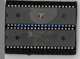
Attack IC PIC16F54 Eeprom
We can attack IC PIC16F54 Eeprom, please view the IC PIC16F54 features for your reference:
High-Performance RISC CPU:
· Only 33 single-word instructions to learn
· All instructions are single cycle except for program branches which are two-cycle
· Two-level deep hardware stack
· Direct, Indirect and Relative Addressing modes for data and instructions
Attack IC PIC16F54 Eeprom
· Operating speed:
– DC – 20 MHz clock speed
– DC – 200 ns instruction cycle time
· On-ic Flash program memory:
– 512 x 12 on PIC16F54
– 2048 x 12 on PIC16F57
– 2048 x 12 on PIC16F59
· General Purpose Registers (SRAM)
– 25 x 8 on PIC16F54
– 72 x 8 on PIC16F57
– 134 x 8 on PIC16F59
Special Microcontroller Features:
· Power-on Reset (POR)
· Device Reset Timer (DRT)
· Watchdog Timer (WDT) with its own on-ic RC oscillator for reliable operation
· Programmable Code Protection to prevent Microcontroller unlocking
· Power-Saving Sleep mode
· In-Circuit Serial Programming™ (ICSP™)
· Selectable oscillator options:
– RC: Low-cost RC oscillator
– XT: Standard crystal/resonator
– HS: High-speed crystal/resonator
– LP: Power-saving, low-frequency crystal
· Packages:
– 18-pin PDIP and SOIC for PIC16F54
– 20-pin SSOP for PIC16F54
– 28-pin PDIP, SOIC and SSOP for PIC16F57
– 40-pin PDIP for PIC16F59
– 44-pin TQFP for PIC16F59
Low-Power Features:
· Operating Current:
– 170 ìA @ 2V, 4 MHz, typical
– 15 ìA @ 2V, 32 kHz, typical
· Standby Current:
– 500 nA @ 2V, typical
Peripheral Features:
· 12/20/32 I/O pins:
– Individual direction control
– High current source/sink
· 8-bit real-time clock/counter (TMR0) with 8-bit programmable prescaler
CMOS Technology:
· Wide operating voltage range:
– Industrial: 2.0V to 5.5V
– Extended: 2.0V to 5.5V
· Wide temperature range:
– Industrial: -40°C to 85°C
– Extended: -40°C to 125°C
· High-endurance Flash:
– 100K write/erase cycles
– > 40-year retention
Break Chip PIC16F59 Eeprom
Break Chip PIC16F59 Eeprom
The high performance of the PIC16F5X family can be attributed to a number of architectural features commonly found in RISC microprocessors to Break Chip PIC16F59 Eeprom. To begin with, the PIC16F5X uses a Harvard architecture in which program and data are accessed on separate buses.
This improves bandwidth over traditional von Neumann architecture where program and data are fetched on the same bus. Separating program and data memory further allows instructions to be sized differently than the 8-bit wide data word. Instruction opcodes are 12-bits wide, making it possible to have all single-word instructions. A 12-bit wide program memory access bus fetches a 12-bit instruction in a single cycle.
A two-stage pipeline overlaps fetch and execution of instructions. Consequently, all instructions (33) execute in a single cycle except for program branches. The PIC16F54 addresses 512 x 12 of program memory, the PIC16F57 and PIC16F59 addresses 2048 x 12 of program memory. All program memory is internal.
The PIC16F5X can directly or indirectly address its register files and data memory. All Special Function Registers (SFR), including the program counter, are mapped in the data memory. The PIC16F5X has a highly orthogonal (symmetrical) instruction set that makes it possible to carry out any operation on any register using any Addressing mode when Break Chip PIC16F59 Eeprom. This symmetrical nature and lack of ‘special optimal situations’ make programming with the PIC16F5X simple, yet efficient. In addition, the learning curve is reduced significantly.
The PIC16F5X device contains an 8-bit ALU and working register. The ALU is a general purpose arithmetic unit. It performs arithmetic and Boolean functions between data in the working register and any register file.
The ALU is 8-bits wide and capable of addition, subtraction, shift and logical operations. Unless otherwise mentioned, arithmetic operations are two’s complement in nature. In two-operand instructions, typically one operand is the W (working) register. The other operand is either a file register or an immediate constant. In single operand instructions, the operand is either the W register or a file register.
The W register is an 8-bit working register used for ALU operations. It is not an addressable register. Depending on the instruction executed, the ALU may affect the values of the Carry (C), Digit Carry (DC) and Zero (Z) bits in the STATUS Register to Extract IC code. The C and DC bits operate as a borrow and digit borrow out bit, respectively, in subtraction. See the SUBWF and ADDWF instructions for examples.
A simplified block diagram is shown in Figure 2-1 with the corresponding device pins described in Table 2-1 (for PIC16F54), Table 2-2 (for PIC16F57) and Table 2-3 (for PIC16F59).