Posts Tagged ‘recover chip encrypted content’
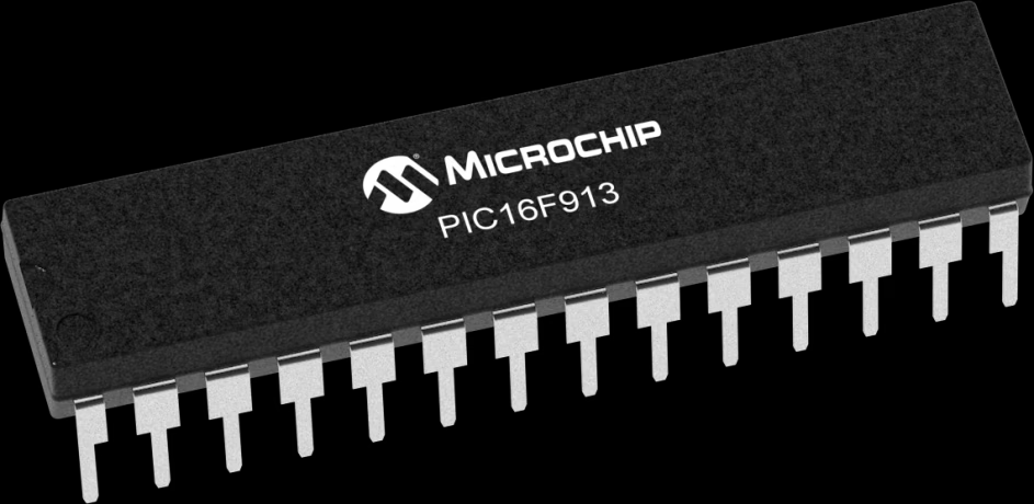
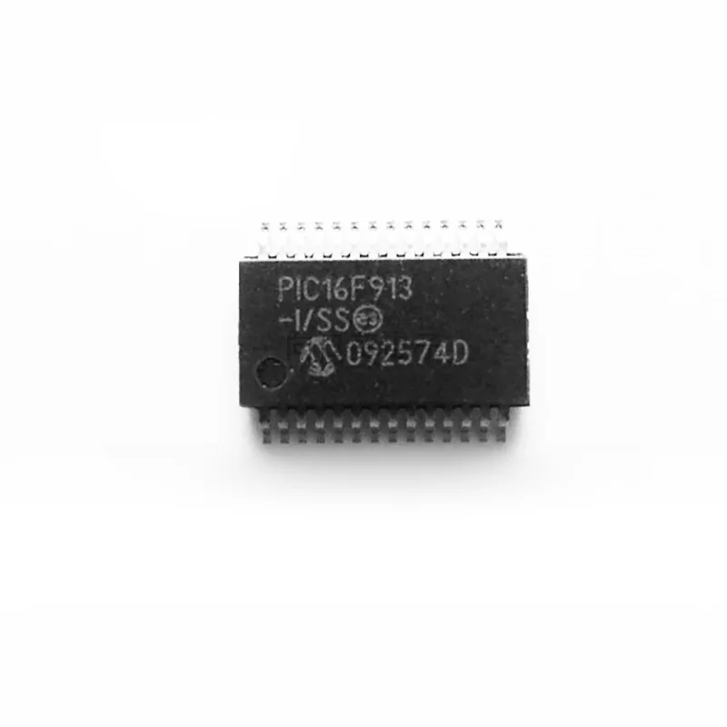
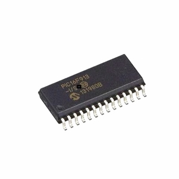
 Recover Chip PIC16F913 Binary
When working with embedded systems, one of the most challenging tasks can be extracting or recovering chip PIC16F913 binary data. This microcontroller, produced by Microchip Technology, is commonly found in remote controls, industrial equipment, and sensor-based systems. Unlike many older or simpler microcontrollers, the PIC16F913 features advanced security mechanisms, making its firmware difficult to access or duplicate without specialized skills and tools.
Podczas pracy z systemami wbudowanymi jednym z najtrudniejszych zadań może być wyodrębnienie lub odzyskanie danych binarnych układu PIC16F913. Ten mikrokontroler, wyprodukowany przez Microchip Technology, jest powszechnie spotykany w pilotach zdalnego sterowania, sprzęcie przemysłowym i systemach opartych na czujnikach. W przeciwieństwie do wielu starszych lub prostszych mikrokontrolerów, PIC16F913 posiada zaawansowane mechanizmy bezpieczeństwa, co utrudnia dostęp do jego oprogramowania układowego lub jego kopiowanie bez specjalistycznych umiejętności i narzędzi.
At CIRCUIT ENGINEERING CO.,LTD we offer professional services to read out, restore, and recover PIC16F913 binaries, whether for software migration, security auditing, or backup purposes. Our process allows clients to unlock, decode, and decrypt protected memory, giving full access to the firmware, EEPROM, or flash data stored inside the microcontroller.
What Makes PIC16F913 Unique?
Compared to simpler chips like the PIC16C554 or PIC12CE519, the PIC16F913 includes:
Extended instruction set (Mid-Range architecture) with more advanced features.
Integrated LCD driver module, making it more common in display-based applications.
More robust memory protection, including locked and encrypted flash/eeprom blocks, making unauthorized binary readouts or program duplication more difficult.
تحليل ثنائي وفك تشفير البرامج الثابتة بمجرد استخراجها، تُحلل الملفات الثنائية أو السداسية لتحديد أنماط التعليمات، ومقاطع البيانات، والهياكل المنطقية. ثم يقوم فريقنا بفك تشفير أرشيف البرامج الثابتة، وإعادة بناء تسلسل الكود الأصلي ومنطقه. استعادة البرامج الثابتة واستعادة الكود المصدري عند الحاجة، نستعيد الكود المصدري من الملف الثنائي المفكك. على الرغم من أن ملف البرنامج المستعاد قد لا يتطابق تمامًا مع الكود الأصلي المكتوب بلغة C، إلا أنه يوفر تمثيلًا قابلاً للاستخدام والقراءة، ويمكن تعديله أو نسخه حسب الحاجة. الاستنساخ والنسخ بعد استعادة البيانات، نساعد عملائنا على استنساخ أو نسخ البرامج الثابتة على شرائح أو أجهزة جديدة. سواءً للنسخ الاحتياطي أو الإنتاج، يتيح هذا النسخ الكامل للبرنامج الأصلي المؤمّن.
On-board comparators, analog modules, and enhanced I/O, increasing complexity of its firmware structure.
This chip’s secured and embedded firmware is designed to prevent unauthorized duplication or tampering. However, with the right techniques, even protected programs and data archives can be successfully recovered.
Recover Chip PIC16F913 Binary is a process of dumping heximal from MCU’s PIC16F913 flash memory, the status of Microcontroller PIC16F913 can be changed from locked to open by MCU Cracking technique
Recover Chip PIC16F913 Binary is a process of dumping heximal from MCU’s PIC16F913 flash memory, the status of Microcontroller PIC16F913 can be changed from locked to open by MCU Cracking technique;
High-Performance RISC CPU:
· Only 35 instructions to learn:
– All single-cycle instructions except branches
· Operating speed:
– DC – 20 MHz oscillator/clock input
– DC – 200 ns instruction cycle
· Program Memory Read (PMR) capability
· Interrupt capability
· 8-level deep hardware stack
· Direct, Indirect and Relative Addressing modes
Special Microcontroller Features:
· Precision Internal Oscillator:
– Factory calibrated to ±1%, typical
– Software selectable frequency range of
8 MHz to 125 kHz
– Software tunable
– Two-Speed Start-up mode
– External Oscillator fail detect for critical applications
– Clock mode switching during operation for power savings
· Software selectable 31 kHz internal oscillator
· Power-Saving Sleep mode
· Wide operating voltage range (2.0V-5.5V)
· Industrial and Extended temperature range
· Power-on Reset (POR)
· Power-up Timer (PWRT) and Oscillator Start-up
Timer (OST)
· Brown-out Reset (BOR) with software control option
· Enhanced Low-Current Watchdog Timer (WDT) with on-chip oscillator (software selectable nominal 268 seconds with full prescaler) with software enable
· Multiplexed Master Clear with pull-up/input pin
· Programmable code protection
· High-Endurance Flash/EEPROM cell:
– 100,000 write Flash endurance
– 1,000,000 write EEPROM endurance
– Flash/Data EEPROM retention: > 40 years
Quando si lavora con sistemi embedded, uno dei compiti più impegnativi può essere l’estrazione o il recupero dei dati binari del chip PIC16F913. Questo microcontrollore, prodotto da Microchip Technology, è comunemente presente in telecomandi, apparecchiature industriali e sistemi basati su sensori. A differenza di molti microcontrollori più vecchi o più semplici, il PIC16F913 è dotato di meccanismi di sicurezza avanzati, che rendono il suo firmware difficile da accedere o duplicare senza competenze e strumenti specializzati.
Low-Power Features:
· Standby Current:
– <100 nA @ 2.0V, typical
· Operating Current:
– 11 ìA @ 32 kHz, 2.0V, typical
– 220 ìA @ 4 MHz, 2.0V, typical
· Watchdog Timer Current:
– 1 ìA @ 2.0V, typical
Peripheral Features:
· Liquid Crystal Display module:
– Up to 60/96/168 pixel drive capability on 28/40/64-pin devices, respectively
– Four commons
· Up to 24/35/53 I/O pins and 1 input-only pin:
– High-current source/sink for direct LED drive
– Interrupt-on-change pin
– Individually programmable weak pull-ups
· In-Circuit Serial Programming™ (ICSP™) via two pins
· Analog comparator module with:
– Two analog comparators
– Programmable on-chip voltage reference (CVREF) module (% of VDD)
– Comparator inputs and outputs externally accessible
· A/D Converter:
– 10-bit resolution and up to 8 channels
· Timer0: 8-bit timer/counter with 8-bit
programmable prescaler
· Enhanced Timer1:
– 16-bit timer/counter with prescaler
– External Timer1 Gate (count enable)
– Option to use OSC1 and OSC2 as Timer1 oscillator if INTOSCIO or LP mode is selected
· Timer2: 8-bit timer/counter with 8-bit period register, prescaler and postscaler
· Addressable Universal Synchronous
Asynchronous Receiver Transmitter (AUSART)
· Up to 2 Capture, Compare, PWM modules:
– 16-bit Capture, max. resolution 12.5 ns
– 16-bit Compare, max. resolution 200 ns
– 10-bit PWM, max. frequency 20 kHz
· Synchronous Serial Port (SSP) with I2C™