Archive for July, 2014
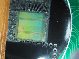
 Recover Microcontroller PIC16F83 Eeprom
We can Recover Microcontroller PIC16F83 Eeprom, please view the Microcontroller PIC16F83 features for your reference:
High Performance RISC CPU Features:
• Only 35 single word instructions to learn
• All instructions single cycle except for program branches which are two-cycle Operating speed: DC – 10 MHz clock input
DC – 400 ns instruction cycle
14-bit wide instructions
8-bit wide data path
15 special function hardware registers
Eight-level deep hardware stack
Direct, indirect and relative addressing modes
Four interrupt sources:
– External RB0/INT pin
– TMR0 timer overflow
– PORTB<7:4> interrupt on change
– Data EEPROM write complete
· 1000 erase/write cycles Flash program memory
· 10,000,000 erase/write cycles EEPROM data memory
· EEPROM Data Retention > 40 years
Peripheral Features:
· 13 I/O pins with individual direction control
· High current sink/source for direct LED drive
– 25 mA sink max. per pin
– 20 mA source max. per pin
· TMR0: 8-bit timer/counter with 8-bit programmable prescaler
Special Microcontroller Features:
· In-Circuit Serial Programming (ICSP™) – via two pins (ROM devices support only Data EEPROM programming)
· Power-on Reset (POR)
· Power-up Timer (PWRT)
· Oscillator Start-up Timer (OST)
· Watchdog Timer (WDT) with its own on-Microcontroller RC oscillator for reliable operation
· Code-protection
· Power saving SLEEP mode
· Selectable oscillator options
Low-power, high-speed technology
· Fully static design
· Wide operating voltage range:
– Commercial: 2.0V to 6.0V
– Industrial: 2.0V to 6.0V
· Low power consumption:
– < 2 mA typical @ 5V, 4 MHz
– 15 µA typical @ 2V, 32 kHz
– < 1 µA typical standby current @ 2V
Circuit Engineering Company Limited continues to be recognized as the Southern China Leader in Services for IC Read, MCU Recover, Microcontroller Extract, Microcontroller Unlock service. With the advancement of today’s modern circuit board technology, it is more important than ever to have specialists available to help you at a moment’s notice. Our engineering and commercial teams collectively have a vast amount of electronic experience covering field include Consumer Electronics, Industrial Automation Electronics, Wireless Communication Electronics., etc. For more information please contact us through email.
Recover MCU PIC16C71 Code
The PIC16C71X is a family of low-cost, high-performance, CMOS, fully-static, 8-bit microcontrollers with integrated analog-to-digital (A/D) converters, in the PIC16CXX mid-range family when it becomes necessary to Recover MCU PIC16C71 Code. All PIC16/17 microcontrollers employ an advanced RISC architecture by Break IC TS83C51U2 Binary. The PIC16CXX microcontroller family has enhanced core features, eight-level deep stack, and multiple internal and external interrupt sources.
Recover MCU PIC16C71 Code
The separate instruction and data buses of the Harvard architecture allow a 14-bit wide instruction word with the separate 8-bit wide data. The two stage instruction pipeline allows all instructions to execute in a single cycle, except for program branches which require two cycles. A total of 35 instructions (reduced instruction set) are available in the process of Crack MCU Program. Additionally, a large register set gives some of the architectural innovations used to achieve a very high performance.
PIC16CXX microcontrollers typically achieve a 2:1 code compression and a 4:1 speed improvement over other 8-bit microcontrollers in their class. The PIC16C71 devices have 36 bytes of RAM, the PIC16C711 has 68 bytes of RAM and the PIC16C715 has 128 bytes of RAM. Each device has 13 I/O pins. In addition a timer/counter is available. Also a 4-channel high-speed 8-bit A/D is provided which provide support for Break IC ATMEGA32A Software.
The 8-bit resolution is ideally suited for applications requiring low-cost analog interface, e.g. thermostat control, pressure sensing, etc. The PIC16C71X family has special features to reduce external components, thus reducing cost, enhancing system reliability and reducing power consumption.
There are four oscillator options, of which the single pin RC oscillator provides a low-cost solution, the LP oscillator minimizes power consumption, XT is a standard crystal, and the HS is for High Speed crystals only in order to Recover MICROCONTROLLER ATMEGA64PA Binary. The SLEEP (power-down) feature provides a power saving mode. The user can wake up the MCU from SLEEP through several external and internal interrupts and resets.
Recover IC PIC16C554 Software
Recover IC PIC16C554 Software
We can Recover IC PIC16C554 Software, please view the Ic PIC16C554 features for your reference:
High Performance RISC CPU:
· Only 35 instructions to learn
· All single-cycle instructions (200 ns), except for program branches which are two-cycle
· Operating speed:
– DC – 20 MHz clock input
– DC – 200 ns instruction cycle
16 special function hardware registers
Special Ic Features (cont’d)
8-level deep hardware stack
Direct, Indirect and Relative addressing modes by Break MCU ATMEGA64PA Binary,
Programmable code protection
Power saving SLEEP mode
Peripheral Features:
· 13 I/O pins with individual direction control
· High current sink/source for direct LED drive Selectable oscillator options Serial in-circuit programming (via two pins) Four user programmable ID locations
· Timer0: 8-bit timer/counter with 8-bit programmable prescaler
Special Ic Features:
· Power-on Reset (POR)
· Power-up Timer (PWRT) and Oscillator Start-up Timer (OST)
· Watchdog Timer (WDT) with its own on-chip RC oscillator for reliable operation
CMOS Technology:
· Low-power, high-speed CMOS EPROM technology when Break MCU ATMEGA128PA Firmware
· Fully static design
· Wide operating voltage range
– 2.5V to 5.5V PIC16C55X
– 3.0 to 5.5V PIC16C55XA
· Commercial, industrial and extended temperature range
· Low power consumption
– < 2.0 mA @ 5.0V, 4.0 MHz
– 15 µA typical @ 3.0V, 32 kHz
– < 1.0 µA typical standby current @ 3.0V from Break IC ATMEGA128A Firmware
Circuit Engineering Company Limited continues to be recognized as the Southern China Leader in Services for IC Read, MCU Crack, MCU Recover, IC Unlock service. With the advancement of today’s modern circuit board technology, it is more important than ever to have specialists available to help you at a moment’s notice. Our engineering and commercial teams collectively have a vast amount of electronic experience covering field include Consumer Electronics, Industrial Automation Electronics, Wireless Communication Electronics., etc. For more
Copy Chip PIC16F74A Binary
Copy Chip PIC16F74A Binary
The high performance of the PIC16CXX family can be attributed to a number of architectural features commonly found in RISC microprocessors. To begin with, the PIC16CXX uses a Harvard architecture, in which, program and data are accessed from separate memories using separate buses to Copy Chip PIC16F74A Binary. This improves bandwidth over traditional von Neumann architecture in which program and data are fetched from the same memory using the same bus.
Separating program and data buses further allows instructions to be sized differently than the 8-bit wide data word. Instruction opcodes are 14-bits wide making it possible to have all single word instructions by Recovery MICROCONTROLLER ATMEGA48A Program. A 14-bit wide program memory access bus fetches a 14-bit instruction in a single cycle.
A two-stage pipeline overlaps fetch and execution of instructions. Consequently, all instructions (35) execute in a single cycle (200 ns @ 20 MHz) except for program branches.
The PIC16CXX can directly or indirectly address its register files or data memory. All special function registers, including the program counter, are mapped in the data memory. The PIC16CXX has an orthogonal (symmetrical) instruction set that makes it possible to carry out any operation on any register using any addressing mode.
This symmetrical nature and lack of ‘special optimal situations’ make programming with the PIC16CXX simple yet efficient. In addition, the learning curve is reduced significantly.
PIC16CXX devices contain an 8-bit ALU and working register. The ALU is a general purpose arithmetic unit to Break MCU ATMEGA168A Flash, It performs arithmetic and Boolean functions between the data in the working register and any register file.
The ALU is 8-bits wide and capable of addition, subtraction, shift and logical operations. Unless otherwise mentioned, arithmetic operations are two’s complement in nature. In two-operand instructions, typically one operand is the working register (W register) from Copy Chip PIC16F74A Binary. The other operand is a file register or an immediate constant.
In single operand instructions, the operand is either the W register or a file register. The W register is an 8-bit working register used for ALU operations. It is not an addressable register. Depending on the instruction executed, the ALU may affect the values of the Carry (C), Digit Carry (DC), and Zero (Z) bits in the STATUS register to Recover IC ATMEGA168PA Program. The C and DC bits operate as a borrow bit and a digit borrow out bit, respectively, in subtraction. See theSUBLW and SUBWF instructions for examples after clone IC.
Copy Microcontroller PIC16C770 Eeprom
Copy Microcontroller PIC16C770 Eeprom
We can Copy Microcontroller PIC16C770 Eeprom, please view the Microcontroller PIC16C770 features for your reference:
This document contains device-specific information. Additional information may be found in the PICmicroTM Mid-Range Reference Manual, (DS33023), which may be obtained from your local Micromicrocontroller Sales Representative or downloaded from the Micromicrocontroller website.
The Reference Manual should be considered a complementary document to this data sheet, and is highly recommended copying for a better understanding of the device architecture and operation of the peripheral modules.
There are two memory blocks in each of these PICmicro ® microcontrollers. Each block (Program Memory and Data Memory) has its own bus, so that concurrent access can occur. Additional information on device memory may be found in the PICmicro Mid-Range Reference Manual, (DS33023).
The PIC16C717/770/771 devices have a 13-bit program counter capable of addressing an 8K x 14 program memory space. The PIC16C717 and the PIC16C770 have 2K x 14 words of program memory. The PIC16C771 has 4K x 14 words of program memory. Accessing a location above the physically implemented address will cause a wraparound which can facilitate the MCU Cracking.
The reset vector is at 0000h and the interrupt vector is at 0004h. Each bank extends up to 7Fh (128 bytes). The lower locations of each bank are reserved for the Special Function Registers. Above the Special Function Registers are General Purpose Registers, implemented as static RAM. All implemented banks contain special function registers if Copy Microcontroller. Some frequently used special function registers from one bank are mirrored in another bank for code reduction and quicker access.
The Special Function Registers are registers used by the CPU and Peripheral Modules for controlling the desired operation of the device. These registers are implemented as static RAM.
The special function registers can be classified into two sets; core (CPU) and peripheral. Those registers associated with the core functions are described in detail in this section. Those related to the operation of the peripheral features are described in detail in that peripheral feature section.
Copy AVR ATmega161 Firmware
Copy AVR ATmega161 Firmware
We can Copy AVR ATMEGA161 Firmware, please view below the feature of AVR ATMEGA161 for our reference:
Features
· High-performance, Low-power AVR® 8-bit Microcontroller
· Advanced RISC Architecture
– 130 Powerful Instructions – Most Single Clock Cycle Execution
– 32 x 8 General Purpose Working Registers
– Fully Static Operation
– Up to 8 MIPS Throughput at 8 MHz
– On-chip 2-cycle Multiplier
Program and Data Memories
– 16K Bytes of Non-volatile In-System Programmable Flash Endurance: 1,000 Write/Erase Cycles
– Optional Boot Code Memory with Independent Lock bits Self-programming of Program and Data Memories
– 512 Bytes of Non-volatile In-System Programmable EEPROM Endurance: 100,000 Write/Erase Cycles
– 1K Byte of Internal SRAM
– Programming Lock for Software Security
Peripheral Features
– Two 8-bit Timer/Counters with Separate Prescaler and PWM
– Expanded 16-bit Timer/Counter System with Separate Prescaler, Compare, Capture Modes and Dual 8-, 9-, or 10-bit PWM after Copy AVR
– Dual Programmable Serial UARTs
– Master/Slave SPI Serial Interface
– Real-time Counter with Separate Oscillator
– Programmable Watchdog Timer with Separate On-chip Oscillator
– On-chip Analog Comparator
Special Microcontroller Features
– External and Internal Interrupt Sources
– Three Sleep Modes: Idle, Power-save and Power-down Power Comsumption at 4 MHz, 3.0V, 25°C
– Active 3.0 mA
– Idle Mode 1.2 mA
– Power-down Mode < 1 µA
I/O and Packages
– 35 Programmable I/O Lines
– 40-lead PDIP and 44-lead TQFP Operating Voltages
– 2.7V – 5.5V for the ATmega161L
– 4.0V – 5.5V for the ATmega161 Speed Grades
– 0 – 4 MHz for the ATmega161L
– 0 – 8 MHz for the ATmega161
Commercial and Industrial Temperature Ranges
Attack AVR ATmega64L Program
Attack AVR ATmega64L Program
We can Attack AVR ATmega64L Program, please view below AVR ATMEGA64L features for your reference:
High-performance, Low-power Atmel® AVR® 8-bit Microcontroller
· Advanced RISC Architecture
– 130 Powerful Instructions – Most Single Clock Cycle Execution
– 32 x 8 General Purpose Working Registers + Peripheral Control Registers
– Fully Static Operation
– Up to 16 MIPS Throughput at 16 MHz
– On-chip 2-cycle Multiplier
High Endurance Non-volatile Memory segments
– 64 Kbytes of In-System Reprogrammable Flash program memory
– 2 Kbytes EEPROM
– 4 Kbytes Internal SRAM
– Write/Erase Cycles: 10,000 Flash/100,000 EEPROM
– Data retention: 20 years at 85°C/100 years at 25°C(1)
– Optional Boot Code Section with Independent Lock Bits
In-System Programming by On-chip Boot Program
True Read-While-Write Operation
– Up to 64 Kbytes Optional External Memory Space
– Programming Lock for Software Security
– SPI Interface for In-System Programming
JTAG (IEEE std. 1149.1 Compliant) Interface
– Boundary-scan Capabilities According to the JTAG Standard
– Extensive On-chip Debug Support
– Programming of Flash, EEPROM, Fuses, and Lock Bits through the JTAG Interface
Peripheral Features
– Two 8-bit Timer/Counters with Separate Prescalers and Compare Modes
– Two Expanded 16-bit Timer/Counters with Separate Prescaler, Compare Mode, and Capture Mode
– Real Time Counter with Separate Oscillator
– Two 8-bit PWM Channels
– 6 PWM Channels with Programmable Resolution from 1 to 16 Bits
– 8-channel, 10-bit ADC
8 Single-ended Channels
7 Differential Channels
2 Differential Channels with Programmable Gain (1x, 10x, 200x)
– Byte-oriented Two-wire Serial Interface
– Dual Programmable Serial USARTs
– Master/Slave SPI Serial Interface
– Programmable Watchdog Timer with On-chip Oscillator before Attack AVR
– On-chip Analog Comparator
Special Microcontroller Features
– Power-on Reset and Programmable Brown-out Detection
– Internal Calibrated RC Oscillator
– External and Internal Interrupt Sources
– Six Sleep Modes: Idle, ADC Noise Reduction, Power-save, Power-down, Standby and Extended Standby
– Software Selectable Clock Frequency
– ATmega103 Compatibility Mode Selected by a Fuse
– Global Pull-up Disable
I/O and Packages
– 53 Programmable I/O Lines
– 64-lead TQFP and 64-pad QFN/MLF
Operating Voltages
– 2.7V – 5.5V for ATmega64L
– 4.5V – 5.5V for ATmega64
Speed Grades
– 0 – 8 MHz for ATmega64L
– 0 – 16 MHz for ATmega64
Copy AVR ATmega165A
Copy AVR ATmega165A
We can Copy AVR ATmega165A, please view below the feature of AVR ATmega165A for your reference:
Features
High Performance, Low Power Atmel® AVR® 8-Bit Microcontroller
Advanced RISC Architecture
– 130 Powerful Instructions – Most Single Clock Cycle Execution
– 32 x 8 General Purpose Working Registers
– Fully Static Operation
– Up to 16MIPS Throughput at 16MHz (ATmega165PA/645P)
– Up to 20MIPS Throughput at 20MHz
(ATmega165A/325A/325PA/645A/3250A/3250PA/6450A/6450P)
– On-Chip 2-cycle Multiplier
High Endurance Non-volatile Memory segments
– In-System Self-programmable Flash Program Memory
· 16KBytes (ATmega165A/ATmega165PA)
· 32KBytes (ATmega325A/ATmega325PA/ATmega3250A/ATmega3250PA)
· 64KBytes (ATmega645A/ATmega645P/ATmega6450A/ATmega6450P)
– EEPROM
· 512Bytes (ATmega165A/ATmega165PA)
· 1Kbytes (ATmega325A/ATmega325PA/ATmega3250A/ATmega3250PA)
· 2Kbytes (ATmega645A/ATmega645P/ATmega6450A/ATmega6450P)
– Internal SRAM
· 1KBytes (ATmega165A/ATmega165PA)
· 2KBytes (ATmega325A/ATmega325PA/ATmega3250A/ATmega3250PA)
· 4KBytes (ATmega645A/ATmega645P/ATmega6450A/ATmega6450P)
– Write/Erase cycles: 10,000 Flash/100,000 EEPROM
– Data retention: 20 years at 85°C/100 years at 25°C(1)
– Optional Boot Code Section with Independent Lock Bits
· In-System Programming by On-chip Boot Program
· True Read-While-Write Operation
– Programming Lock for Software Security
– Capacitive touch buttons, sliders and wheels
– Up to 64 sense channels
JTAG (IEEE std. 1149.1 compliant) Interface
– Boundary-scan Capabilities According to the JTAG Standard
– Extensive On-chip Debug Support
– Programming of Flash, EEPROM, Fuses, and Lock Bits through the JTAG Interface
Peripheral Features
– Two 8-bit Timer/Counters with Separate Prescaler and Compare Mode
– One 16-bit Timer/Counter with Separate Prescaler, Compare Mode, and Capture Mode
– Real Time Counter with Separate Oscillator
– Four PWM Channels
– 8-channel, 10-bit ADC
– Programmable Serial USART
– Master/Slave SPI Serial Interface
– Universal Serial Interface with Start Condition Detector
– Programmable Watchdog Timer with Separate On-chip Oscillator
– On-chip Analog Comparator
– Interrupt and Wake-up on Pin Change
Special Microcontroller Features
– Power-on Reset and Programmable Brown-out Detection
– Internal Calibrated Oscillator
– External and Internal Interrupt Sources
– Five Sleep Modes: Idle, ADC Noise Reduction, Power-save, Power-down, and Standby
I/O and Packages
– 54/69 Programmable I/O Lines
– 64/100-lead TQFP, 64-pad QFN/MLF and 64-pad DRQFN
Speed Grade:
– ATmega 165A/165PA/645A/645P: 0 – 16MHz @ 1.8 – 5.5V
– ATmega325A/325PA/3250A/3250PA/6450A/6450P: 0 – 20MHz @ 1.8 – 5.5V
Temperature range:
– -40°C to 85°C Industrial
Ultra-Low Power Consumption (picoPower devices)
– Active Mode:
· 1MHz, 1.8V: 215µA
· 32kHz, 1.8V: 8µA (including Oscillator)
– Power-down Mode: 0.1µA at 1.8V
– Power-save Mode: 0.6µA at 1.8V (Including 32kHz RTC over 20 years at 85°C or 100 years at 25°C
Attack IC LPC2119FBD64 Firmware
Attack IC LPC2119FBD64 Firmware
We can Attack IC LPC2119FBD64 Firmware, please view below IC LPC2119FBD64 features for your reference:
16/32-bit ARM7TDMI-S microcontroller in a tiny LQFP64 package.
16 kB on-chip Static RAM.
128/256 kB on-chip Flash Program Memory. 128-bit wide interface/accelerator enables high speed 60 MHz operation. In-System Programming (ISP) and In-Application Programming (IAP) via on-chip boot-loader software. Flash programming takes 1 ms per 512 byte line. Single sector or full chip erase takes 400 ms
EmbeddedICE-RT interface enables breakpoints and watch points. Interrupt service routines can continue to execute while the foreground task is debugged with the on-chip RealMonitor™ software.
Embedded Trace Macrocell enables non-intrusive high speed real-time tracing of instruction execution
Two interconnected CAN interfaces with advanced acceptance filters.
Four channel 10-bit A/D converter with conversion time as low as 2.44 µs.
Multiple serial interfaces including two UARTs (16C550), Fast I2C (400 kbits/s) and two SPIs 60 MHz maximum CPU clock available from programmable on-chip
Phase-Locked Loop with settling time of 100 µs.
Vectored Interrupt Controller with configurable priorities and vector addresses.
Two 32-bit timers (with four capture and four compare channels), PWM unit (six outputs), Real Time Clock and Watchdog
Up to forty-six 5 V tolerant general purpose I/O pins. Up to nine edge or level sensitive external interrupt pins available.
On-chip crystal oscillator with an operating range of 1 MHz to 30 MHz
Two low power modes, Idle and Power-down.
Processor wake-up from Power-down mode via external interrupt.
Individual enable/disable of peripheral functions for power optimization.
Dual power supply:
CPU operating voltage range of 1.65 V to 1.95 V (1.8 V ±0.15 V).
I/O power supply range of 3.0 V to 3.6 V (3.3 V ± 10 %) with 5 V tolerant I/O pads.
Break Chip ATmega48PA Heximal
Break Chip ATmega48PA Heximal
We can Break Chip ATMEGA48PA Heximal, please view below Chip ATMEGA48PA Features for your reference:
· High Performance, Low Power AVR® 8-Bit Microcontroller
· Advanced RISC Architecture
– 131 Powerful Instructions – Most Single Clock Cycle Execution
– 32 x 8 General Purpose Working Registers
– Fully Static Operation
– Up to 20 MIPS Throughput at 20 MHz
– On-chip 2-cycle Multiplier
– 4/8/16/32K Bytes of In-System Self-Programmable Flash progam memory (ATmega48PA/88PA/168PA/328P)
– 256/512/512/1K Bytes EEPROM (ATmega48PA/88PA/168PA/328P)
– 512/1K/1K/2K Bytes Internal SRAM (ATmega48PA/88PA/168PA/328P)
– Write/Erase Cycles: 10,000 Flash/100,000 EEPROM
– Data retention: 20 years at 85°C/100 years at 25°C(1)
– Optional Boot Code Section with Independent Lock Bits
In-System Programming by On-chip Boot Program
True Read-While-Write Operation
– Programming Lock for Software Security
Peripheral Features
– Two 8-bit Timer/Counters with Separate Prescaler and Compare Mode
– One 16-bit Timer/Counter with Separate Prescaler, Compare Mode, and Capture Mode
– Real Time Counter with Separate Oscillator
– Six PWM Channels
– 8-channel 10-bit ADC in TQFP and QFN/MLF package
Temperature Measurement
– 6-channel 10-bit ADC in PDIP Package
Temperature Measurement
– Programmable Serial USART
– Master/Slave SPI Serial Interface
– Byte-oriented 2-wire Serial Interface (Philips I2C compatible)
– Programmable Watchdog Timer with Separate On-chip Oscillator
– On-chip Analog Comparator
– Interrupt and Wake-up on Pin Change
Special Microcontroller Features
– Power-on Reset and Programmable Brown-out Detection
– Internal Calibrated Oscillator
– External and Internal Interrupt Sources
– Six Sleep Modes: Idle, ADC Noise Reduction, Power-save, Power-down, Standby, and Extended Standby I/O and Packages
– 23 Programmable I/O Lines
– 28-pin PDIP, 32-lead TQFP, 28-pad QFN/MLF and 32-pad QFN/MLF
Operating Voltage:
– 1.8 – 5.5V for ATmega48PA/88PA/168PA/328P
Temperature Range:
– -40°C to 85°C
Speed Grade:
– 0 – 20 MHz @ 1.8 – 5.5V
Low Power Consumption at 1 MHz, 1.8V, 25°C for ATmega48PA/88PA/168PA/328P:
Programmable Flash
ATmega48PA
ATmega88PA
ATmega168PA
ATmega328P
– Active Mode: 0.2 mA
– Power-down Mode: 0.1 µA
– Power-save Mode: 0.75 µA (Including 32 kHz RTC)