Archive for September, 2010
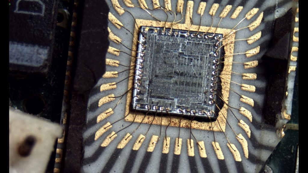
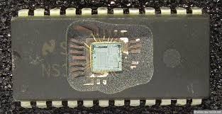
 Reverse Engineering Microcontroller ATMEGA1281 Program
Reverse Engineering Microcontroller ATMEGA1281 purpose is to unlock mcu atmega1281 flash memory and then copy Program and data from atmega1281 memory to new MCU;
Features
High Performance, Low Power AVR® 8-Bit Microcontroller
Advanced RISC Architecture
– 135 Powerful Instructions – Most Single Clock Cycle Execution
– 32 x 8 General Purpose Working Registers
– Fully Static Operation
– Up to 16 MIPS Throughput at 16 MHz
– On-Chip 2-cycle Multiplier
Non-volatile Program and Data Memories
– 64K/128K/256K Bytes of In-System Self-Programmable Flash
Endurance: 10,000 Write/Erase Cycles
– Optional Boot Code Section with Independent Lock Bits
In-System Programming by On-chip Boot Program
True Read-While-Write Operation
– 4K Bytes EEPROM
Endurance: 100,000 Write/Erase Cycles
– 8K Bytes Internal SRAM
– Up to 64K Bytes Optional External Memory Space
– Programming Lock for Software Security
JTAG (IEEE std. 1149.1 compliant) Interface
– Boundary-scan Capabilities According to the JTAG Standard
– Extensive On-chip Debug Support when copy cpld epm9320arc208
– Programming of Flash, EEPROM, Fuses, and Lock Bits through the JTAG Interface
Peripheral Features
– Two 8-bit Timer/Counters with Separate Prescaler and Compare Mode
– Four 16-bit Timer/Counter with Separate Prescaler, Compare- and Capture Mode
– Real Time Counter with Separate Oscillator
– Four 8-bit PWM Channels
– Six/Twelve PWM Channels with Programmable Resolution from 2 to 16 Bits (ATmega1281/2561, ATmega640/1280/2560)
– Output Compare Modulator
– 8/16-channel, 10-bit ADC
– Two/Four Programmable Serial USART (ATmega1281/2561,ATmega640/1280/2560)
– Master/Slave SPI Serial Interface
– Byte Oriented 2-wire Serial Interface
– Programmable Watchdog Timer with Separate On-chip Oscillator after Reverse engineering Microcontroller
– On-chip Analog Comparator
– Interrupt and Wake-up on Pin Change
Special Microcontroller Features
– Power-on Reset and Programmable Brown-out Detection
– Internal Calibrated Oscillator
– External and Internal Interrupt Sources when Reverse engineering Microcontroller
– Six Sleep Modes: Idle, ADC Noise Reduction, Power-save, Power-down, Standby, and Extended Standby
I/O and Packages
– 51/86 Programmable I/O Lines (ATmega1281/2561, ATmega640/1280/2560)
– 64-lead (ATmega1281/2561)
– 100-lead (ATmega640/1280/2560)
– 100-lead TQFP (64-lead TQFP Option)
Temperature Range:
– -40°C to 85°C Industrial if Reverse engineering Microcontroller
Speed Grade:
Programmable Flash
– ATmega1281/2561V/ATmega640/1280/2560V: 0 – 4 MHz @ 1.8 – 5.5V, 0 – 8 MHz @ 2.7 – 5.5V
– ATmega640/1280/1281/2560/2561: 0 – 8 MHz @ 2.7 – 5.5V, 0 – 16 MHz @ 4.5 – 5.5V before Reverse engineering Microcontroller
Recover MCU SN8P2608 Heximal
Recover MCU SN8P2608 Heximal
We can Recover MCU SN8P2608 Heximal, please view the Recover MCU SN8P2608 features for your reference:
The brown out reset is a power dropping condition. The power drops from normal voltage to low voltage by external factors (e.g. EFT interference or external loading changed). The brown out reset would make the system not work well or executing program error when Recover MCU .
The power dropping might through the voltage range that’s the system dead-band. The dead-band means the power range can’t offer the system minimum operation power requirement. The above diagram is a typical brown out reset diagram. There is a serious noise under the VDD, and VDD voltage drops very deep if Recover MCU .
There is a dotted line to separate the system working area. The above area is the system work well area. The below area is the system work error area called dead-band. V1 doesn’t touch the below area and not effect the system operation. But the V2 and V3 is under the below area and may induce the system error occurrence. Let system under dead-band includes some conditions before Recover MCU .
DC application:
The power source of DC application is usually using battery. When low battery condition and MCU drive any loading, the power drops and keeps in dead-band. Under the situation, the power won’t drop deeper and not touch the system reset voltage. That makes the system under dead-band after Recover MCU .
AC application:
In AC power application, the DC power is regulated from AC power source. This kind of power usually couples with AC noise that makes the DC power dirty. Or the external loading is very heavy, e.g. driving motor. The loading operating induces noise and overlaps with the DC power. VDD drops by the noise, and the system works under unstable power situation if Recover MCU .
The power on duration and power down duration are longer in AC application. The system power on sequence protects the power on successful, but the power down situation is like DC low battery condition. When turn off the AC power, the VDD drops slowly and through the dead-band for a while before Recover MCU .
To improve the brown out reset needs to know the system minimum operating voltage which is depend on the system executing rate and power level. Different system executing rates have different system minimum operating voltage after Recover MCU .
The electrical characteristic section shows the system voltage to executing rate relationship. Normally the system operation voltage area is higher than the system reset voltage to VDD, and the reset voltage is decided by LVD detect level if Recover MCU .
The system minimum operating voltage rises when the system executing rate upper even higher than system reset voltage. The dead-band definition is the system minimum operating voltage above the system reset voltage when Recover MCU .
Break IC PIC16C556A Software
Break IC PIC16C556A and make mcu pic16c556a clone which is provide the same functions as original one after read microcontroller Software from embedded memory;
Table 1-1 shows the features of the PIC16C55X(A) mid-range microcontroller families. A simplified block diagram of the PIC16C55X(A) is shown in Figure 3-1.
The PIC16C55X(A) series fit perfectly in applications ranging from motor control to low-power remote sensors. The EPROM technology makes customization of application programs (detection levels, pulse generation, timers, etc.) extremely fast and convenient. The small footprint packages make this microcontroller series perfect for all applications with space limitations.
Low-cost, low-power, high-performance, ease of use and I/O flexibility make the PIC16C55X(A) very versatile.
Those users familiar with the PIC16C5X family of microcontrollers will realize that this is an enhanced version of the PIC16C5X architecture. Please refer to Appendix A for a detailed list of enhancements. Code written for PIC16C5X can be easily ported to PIC16C55X(A) family of devices (Appendix B).
The PIC16C55X(A) family fills the niche for users wanting to migrate up from the PIC16C5X family and not needing various peripheral features of other members of the PIC16XX mid-range microcontroller family.
The PIC16C55X(A) family is supported by a full-featured macro assembler, a software simulator, an in-circuit emulator, a low-cost development programmer and a full-featured programmer. A “C” compiler and fuzzy logic support tools are also available.
A variety of frequency ranges and packaging options are available. Depending on application and production requirements the proper device option can be selected using the information in the PIC16C55X(A) Product Identification System section at the end of this data sheet. When placing orders, please use this page of the data sheet to specify the correct part number.
Break IC SN8P2606 Binary
We can Break IC SN8P2606 Binary, please view the IC SN8P2606 features for your reference:
The power on reset depend no LVD operation for most power-up situations. The power supplying to system is a rising curve and needs some time to achieve the normal voltage. Power on reset sequence is as following:
Power-up: System detects the power voltage up and waits for power stable.
External reset (only external reset pin enable): System checks external reset pin status. If external reset pin is not high level, the system keeps reset status and waits external reset pin released if Break IC SN8P2606 Binary.
System initialization: All system registers is set as initial conditions and system is ready.
Oscillator warm up: Oscillator operation is successfully and supply to system clock.
Program executing: Power on sequence is finished and program executes from ORG 0.
Watchdog reset is a system protection. In normal condition, system works well and clears watchdog timer by program.
Under error condition, system is in unknown situation and watchdog can’t be clear by program before watchdog timer overflow. Watchdog timer overflow occurs and the system is reset. After watchdog reset, the system restarts and returns normal mode. Watchdog reset sequence is as following.
Watchdog timer status: System checks watchdog timer overflow status. If watchdog timer overflow occurs, the system is reset before Break IC SN8P2606 Binary.
System initialization: All system registers is set as initial conditions and system is ready.
Oscillator warm up: Oscillator operation is successfully and supply to system clock.
Program executing: Power on sequence is finished and program executes from ORG 0 when Break IC SN8P2606 Binary.
Watchdog reset is a system protection. In normal condition, system works well and clears watchdog timer by program.
Under error condition, system is in unknown situation and watchdog can’t be clear by program before watchdog timer overflow. Watchdog timer overflow occurs and the system is reset. After watchdog reset, the system restarts and returns normal mode. Watchdog reset sequence is as following.
Watchdog timer status: System checks watchdog timer overflow status. If watchdog timer overflow occurs, the system is reset.
System initialization: All system registers is set as initial conditions and system is ready.
Oscillator warm up: Oscillator operation is successfully and supply to system clock.
Program executing: Power on sequence is finished and program executes from ORG 0. Watchdog timer application note is as following after Break IC SN8P2606 Binary.
Before clearing watchdog timer, check I/O status and check RAM contents can improve system error. Don’t clear watchdog timer in interrupt vector and interrupt service routine. That can improve main routine fail. Clearing watchdog timer program is only at one part of the program. This way is the best structure to enhance the watchdog timer function.
Break Chip PIC12CE518 Binary
Break Chip PIC12CE518 Flash memory and read pic12ce518 mcu binary from embedded memory after copy the embedded code to new microcontroller;
As a program instruction is executed, the Program Counter (PC) will contain the address of the next program instruction to be executed. The PC value is increased by one every instruction cycle, unless an instruction changes the PC.
For a GOTO instruction, bits 8:0 of the PC are provided by the GOTO instruction word. The PC Latch (PCL) is mapped to PC<7:0>. Bit 5 of the STATUS register provides page information to bit 9 of the PC (Figure 4- 8) if extract pic16f84 mcu firmware.
For a CALL instruction, or any instruction where the PCL is the destination, bits 7:0 of the PC again are provided by the instruction word. However, PC<8> does not come from the instruction word, but is always cleared.
Instructions where the PCL is the destination, or Modify PCL instructions, include MOVWF PC, ADDWF PC, and BSF PC,5.
The Program Counter is set upon a RESET, which means that the PC addresses the last location in the last page i.e., the oscillator calibration instruction. After executing MOVLW XX, the PC will roll over to location 00h, and begin executing user code.
The STATUS register page preselect bits are cleared upon a RESET, which means that page 0 is pre-selected.
Therefore, upon a RESET, a GOTO instruction will automatically cause the program to jump to page 0 until the value of the page bits is altered. PIC12C5XX devices have a 12-bit wide L.I.F.O. hardware push/pop stack.
A CALL instruction will push the current value of stack 1 into stack 2 and then push the current program counter value, incremented by one, into stack level 1. If more than two sequential CALL’s are executed, only the most recent two return addresses are stored when crack mc68hc05b6 Chip.
ARETLW instruction will pop the contents of stack level 1 into the program counter and then copy stack level contents into level 1. If more than two sequential RETLW’s are executed, the stack will be filled with the address previously stored in level 2. Note that the W register will be loaded with the literal value specified in the instruction. This is particularly useful for the implementation of data look-up tables within the program memory.
Upon any reset, the contents of the stack remain unchanged, however the program counter (PCL) will also be reset to Break MCU Chip.
Copy Microcontroller PIC16F882 Heximal
Copy Microcontroller PIC16F882 Heximal from flash memory and eeprom memory, unlock mcu pic16f882 protection and crack microcontroller pic16f882 security fuse bit to unleash embedded firmware.
High-Performance RISC CPU:
· Only 35 Instructions to Learn:
– All single-cycle instructions except branches
· Operating Speed:
– DC – 20 MHz oscillator/clock input
– DC – 200 ns instruction cycle
· Interrupt Capability
· 8-Level Deep Hardware Stack
· Direct, Indirect and Relative Addressing modes
Special Microcontroller Features:
· Precision Internal Oscillator:
– Factory calibrated to ±1%
– Software selectable frequency range of 8 MHz to 31 kHz
– Software tunable
– Two-Speed Start-up mode
– Crystal fail detect for critical applications
– Clock mode switching during operation for power savings
· Power-Saving Sleep mode
· Wide Operating Voltage Range (2.0V-5.5V)
· Industrial and Extended Temperature Range
· Power-on Reset (POR)
· Power-up Timer (PWRT) and Oscillator Start-up Timer (OST)
· Brown-out Reset (BOR) with Software Control Option
· Enhanced Low-Current Watchdog Timer (WDT) with On-Chip Oscillator (software selectable nominal 268 seconds with full prescaler) with software enable
· Multiplexed Master Clear with Pull-up/Input Pin
· Programmable Code Protection
· High Endurance Flash/EEPROM Cell:
– 100,000 write Flash endurance
– 1,000,000 write EEPROM endurance
– Flash/Data EEPROM retention: > 40 years
· Program Memory Read/Write during run time
· In-Circuit Debugger (on board)
Reverse Engineering Microcontroller ATMEGA2560V Firmware
We can Reverse engineering Microcontroller ATMEGA2560V Firmware, please view the Microcontroller ATMEGA2560V features for your reference:
The ATmega2560v implements 256 bytes of RAM. The upper 128 bytes of RAM occupy a parallel space to the Special Function Registers. That means the upper 128 bytes have the same addresses as the SFR space but are physically separate from SFR space.
When an instruction accesses an internal location above address 7FH, the address mode used in the instruction specifies whether the CPU accesses the upper 128 bytes of RAM or the SFR space. Instructions that use direct addressing access SFR space.
For example, the following direct addressing instruction accesses the SFR at location 0A0H (which is P2). MOV 0A0H, #data
Instructions that use indirect addressing access the upper 128 bytes of RAM. For example, the following indirect addressing instruction, where R0 contains 0A0H, accesses the data byte at address 0A0H, rather than P2 (whose address is 0A0H) before Reverse Engineering Microcontroller ATMEGA2560V Firmware.
Note that stack operations are examples of indirect addressing, so the upper 128 bytes of data RAM are available as stack, The programmable Watchdog Timer (WDT) operates from an independent oscillator. The prescaler bits, PS0, PS1 and PS2 in SFR WCON are used to set the period of the Watchdog Timer from 16 ms to 2048 ms.
The available timer periods are shown in the following table and the actual timer periods (at VCC = 5V) are within ±30% of the nominal. The WDT is disabled by Power-on Reset and during Power Down. It is enabled by setting the WDTEN bit in SFR WCON (address = 96H) after Reverse Engineering Microcontroller ATMEGA2560V Firmware.
The WDT is reset by setting the WDTRST bit in WCON. When the WDT times out without being reset or disabled, an internal RST pulse is generated to reset the CPU. Table 7. Watchdog Timer Period Selection space.
Timer 0 and Timer 1 in the AT89LS53 operate the same way as Timer 0 and Timer 1 in the AT89C51, AT89C52 and AT89C55. For further information, see the October 1995 Microcontroller Data Book, page 2-45, section titled, “Timer/Counters.”
Timer 2 is a 16 bit Timer/Counter that can operate as either a timer or an event counter. The type of operation is selected by bit C/T2 in the SFR T2CON (shown in Table 2). Timer 2 has three operating modes: capture, auto-reload (up or down counting), and baud rate generator before Reverse Engineering Microcontroller ATMEGA2560V Firmware.
The modes are selected by bits in T2CON, as shown in Table 8. Timer 2 consists of two 8-bit registers, TH2 and TL2. In the Timer function, the TL2 register is incremented every machine cycle. Since a machine cycle consists of 12 oscillator periods, the count rate is 1/12 of the oscillator frequency.
In the Counter function, the register is incremented in response to a 1-to-0 transition at its corresponding external input pin, T2. In this function, the external input is sampled during S5P2 of every machine cycle. When the samples show a high in one cycle and a low in the next cycle, the count is incremented.
The new count value appears in the register during S3P1 of the cycle following the one in which the transition was detected. Since two machine cycles (24 oscillator periods) are required to recognize a 1-to-0 transition, the maximum count rate is 1/24 of the oscillator frequency. To ensure that a given level is sampled at least once before it changes, the level should be held for at least one full machine cycle when Reverse Engineering Microcontroller ATMEGA2560V Firmware.
Recover MCU ATmega2560 Flash
Recover MCU ATmega2560 Flash content and eeprom content, and then make microcontroller atmega2560 cloning after reprogramme the firmware to new MCU, read the firmware from mcu atmega2560 memory;
XTAL1 and XTAL2 are the input and output, respectively, of an inverting amplifier which can be configured for use as an on-chip oscillator, as shown in Figure 1. Either a quartz crystal or ceramic resonator may be used. To drive the device from an external clock source, XTAL2 should be left unconnected while XTAL1 is driven as shown in Figure 2.
There are no requirements on the duty cycle of the external clock signal, since the input to the internal clocking circuitry is through a divide-by-two flip-flop, but minimum and maximum voltage high and low time specifications must be observed if break pic16f631 Mcu .
In idle mode, the CPU puts itself to sleep while all the on-chip peripherals remain active. The mode is invoked by software. The content of the on-chip RAM and all the special functions registers remain unchanged during this mode. The idle mode can be terminated by any enabled interrupt or by a hardware reset. It should be noted that when idle is terminated by a hard ware reset, the device normally resumes program execution, from where it left off, up to two machine cycles before the internal reset algorithm takes control after break microcontroller pic16f628a.
On-chip hardware inhibits access to internal RAM in this event, but access to the port pins is not inhibited. To eliminate the possibility of nated. The only exit from power down is a hardware reset. Reset redefines the SFRs but does not change the on-chip RAM. The reset should not be activated before VCC is restored to its normal operating level and must be held active long enough to allow the oscillator to restart and stabilize.
On the chip are three lock bits which can be left unprogrammed (U) or can be programmed (P) to obtain the additional features listed in the table below:
When lock bit 1 is programmed, the logic level at the EA pin is sampled and latched during reset. If the device is powered up without a reset, the latch initializes to a random value, and holds that value until reset is activated. It is necessary that the latched value of EA be in agreement with the current logic level at that pin in order for the device to function properly before RECOVER MCU.
Recover MCU ATmega1280V Program
Recover MCU ATmega1280V Program from secured eeprom and flash memory, crack microcontroller atmega1280v fuse bit and readout the embedded firmware in the format of heximal from mcu atmega1280v;
1. Non-Recover-While-Write area of flash not functional
Part does not work under 2.4 volts
Incorrect ADC recovering in differential mode
Internal ADC reference has too low value
IN/OUT instructions may be executed twice when Stack is in external RAM
EEPROM recover from application code does not work in Lock Bit Mode 3
Non-Recover-While-Write area of flash not functional if copy microcontroller pic16c771 firmware
The Non-Recover-While-Write area of the flash is not working as expected. The problem is related to the speed of the part when recovering the flash of this area.
Problem Fix/Workaround
– Only use the first 248K of the flash.
– If boot functionality is needed, run the code in the Non-Recover-While-Write area at maximum
1/4th of the maximum frequency of the device at any given voltage. This is done by writing the CLKPR register before entering the boot section of the code
Part does not work under 2.4 volts
The part does not execute code correctly below 2.4 volts
Problem Fix/Workaround
Do not use the part at voltages below 2.4 volts.
Incorrect ADC recovering in differential mode
The ADC has high noise in differential mode. It can give up to 7 LSB error.
Problem Fix/Workaround
Use only the 7 MSB of the result when using the ADC in differential mode after Recover pic16c73b MCU firmware.
Internal ADC reference has too low value
The internal ADC reference has a value lower than specified
Problem Fix/Workaround
– Use AVCC or external reference
– The actual value of the reference can be measured by applying a known voltage to the
ADC when using the internal reference. The result when doing later conversions can then be calibrated.
IN/OUT instructions may be executed twice when Stack is in external RAM
If either an IN or an OUT instruction is executed directly before an interrupt occurs and the stack pointer is located in external ram, the instruction will be executed twice. In some cases this will cause a problem, for example:
– If recovering SREG it will appear that the I-flag is cleared.
– If writing to the PIN registers, the port will toggle twice.
– If recovering registers with interrupt flags, the flags will appear to be cleared.
Problem Fix/Workaround
There are two application work-arounds, where selecting one of them, will be omitting the issue:
– Replace IN and OUT with LD/LDS/LDD and ST/STS/STD instructions
– Use internal RAM for stack pointer.
EEPROM recover from application code does not work in Lock Bit Mode 3 after Recover MCU program.
When the Memory Lock Bits LB2 and LB1 are programmed to mode 3, EEPROM recover does not work from the application code.
Problem Fix/Workaround
Do not set Lock Bit Protection Mode 3 when the application code needs to recover from EEPROM.
Break IC ATmega1280 Eeprom
Break IC ATmega1280 Eeprom and read the firmware from mcu atmega1280 memory, and crack microcontroller atmega1280 security fuse bit by focus ion beam technology;
Port A is an 8-bit bi-directional I/O port with internal pull-up resistors (selected for each bit). The Port A output buffers have symmetrical drive characteristics with both high sink and source capability. As inputs, Port A pins that are externally pulled low will source current if the pull-up resistors are activated.
The Port A pins are tri-stated when a reset condition becomes active, even if the clock is not running. Port B is an 8-bit bi-directional I/O port with internal pull-up resistors (selected for each bit). The Port B output buffers have symmetrical drive characteristics with both high sink and source capability if recover mcu pic18f452 program.
As inputs, Port B pins that are externally pulled low will source current if the pull-up resistors are activated. The Port B pins are tri-stated when a reset condition becomes active, even if the clock is not running.
Port C is an 8-bit bi-directional I/O port with internal pull-up resistors (selected for each bit). The Port C output buffers have symmetrical drive characteristics with both high sink and source capability. As inputs, Port C pins that are externally pulled low will source current if the pull-up resistors are activated. The Port C pins are tri-stated when a reset condition becomes active, even if the clock is not running.
Port D is an 8-bit bi-directional I/O port with internal pull-up resistors (selected for each bit). The Port D output buffers have symmetrical drive characteristics with both high sink and source capability. As inputs, Port D pins that are externally pulled low will source current if the pull-up resistors are activated.
The Port D pins are tri-stated when a reset condition becomes active, even if the clock is not running. Port E is an 8-bit bi-directional I/O port with internal pull-up resistors (selected for each bit). The Port E output buffers have symmetrical drive characteristics with both high sink and source capability.
As inputs, Port E pins that are externally pulled low will source current if the pull-up resistors are activated. The Port E pins are tri-stated when a reset condition becomes active, even if the clock is not running.
Port F serves as analog inputs to the A/D Converter. Port F also serves as an 8-bit bi-directional I/O port, if the A/D Converter is not used. Port pins can provide internal pull-up resistors (selected for each bit). The Port F output buffers have symmetrical drive characteristics with both high sink and source capability after Break IC.
As inputs, Port F pins that are externally pulled low will source current if the pull-up resistors are activated. The Port F pins are tri-stated when a reset condition becomes active, even if the clock is not running. If the JTAG interface is enabled, the pull-up resistors on pins PF7(TDI), PF5(TMS), and PF4(TCK) will be activated even if a reset occurs.
Port G is a 6-bit I/O port with internal pull-up resistors (selected for each bit). The Port G output buffers have symmetrical drive characteristics with both high sink and source capability. As inputs, Port G pins that are externally pulled low will source current if the pull-up resistors are activated. The Port G pins are tri-stated when a reset condition becomes active, even if the clock is not running.
Port H is a 8-bit bi-directional I/O port with internal pull-up resistors (selected for each bit). The Port H output buffers have symmetrical drive characteristics with both high sink and source capability. As inputs, Port H pins that are externally pulled low will source current if the pull-up resistors are activated. The Port H pins are tri-stated when a reset condition becomes active, even if the clock is not running.