Archive for May, 2010
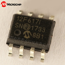
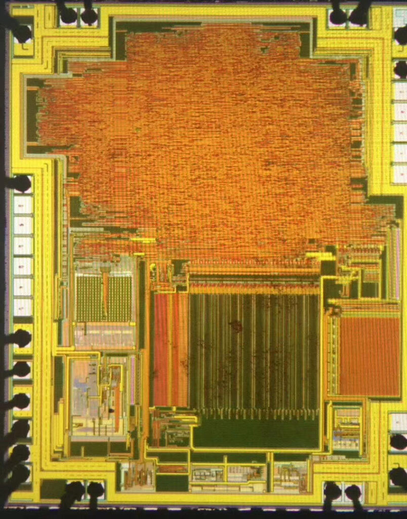
 Break IC PIC12HV615 Heximal
Break IC PIC12HV615 Heximal
We can Break IC PIC12HV615 Heximal, please view the IC PIC12HV615 features for your reference:
To read a program memory location, the user must write two bytes of the address to the PMADRL and PMADRH registers, and then set control bit RD (PMCON1<0>). Once the read control bit is set, the program memory Flash controller will use the second instruction cycle after to read the data.
This causes the second instruction immediately following the “BSF PMCON1,RD” instruction to be ignored. The data is available in the very next cycle in the PMDATL and PMDATH registers; it can be read as two bytes in the following instructions.
PMDATL and PMDATH registers will hold this value until another read or until it is written to by the user (during a write operation). A word of the Flash program memory may only be written to if the word is in an unprotected segment of memory after Break IC.
Flash program memory must be written in four-word blocks. See Figure 3-2 and Figure 3-3 for more details. A block consists of four words with sequential addresses, with a lower boundary defined by an address, where PMADRL<1:0> = 00. All block writes to program memory are done as 16-word erase by four-word write operations. The write operation is edge aligned and cannot occur across boundaries. To write program data, it must first be loaded into the buffer registers (see Figure 3-2). This is accomplished by first writing the destination address to PMADRL and PMADRH and then writing the data to PMDATL and PMDATH.
After the address and data have been set up, then the following sequence of events must be executed:
Write 55h, then AAh, to PMCON2 (Flash programming sequence). Set the WR control bit of the PMCON1 register. All four buffer register locations should be written to with correct data. If less than four words are being written to in the block of four words, then a read from the program memory location(s) not being written to must be performed if Break IC.
This takes the data from the program location(s) not being written and loads it into the PMDATL and PMDATH registers. Then the sequence of events to transfer data to the buffer registers must be executed. To transfer data from the buffer registers to the program memory, the PMADRL and PMADRH must point to the last location in the four-word block (PMADRL<1:0> = 11). Then the following sequence of events must be executed:
Write 55h, then AAh, to PMCON2 (Flash programming sequence). Set control bit WR of the PMCON1 register to begin the write operation. The user must follow the same specific sequence to initiate the write for each word in the program block, writing each program word in sequence (000, 001, 010, 011). When the write is performed on the last word (PMADRL<1:0> = 11), a block of sixteen words is automatically erased and the content of the four-word buffer registers are written into the program memory. After the “BSF PMCON1,WR” instruction, the processor requires two cycles to set up the erase/write operation. The user must place two NOP instructions after the WR bit is set. Since data is being written to buffer registers, the writing of the first three words of the block appears to occur immediately before Break IC.
Break Chip PIC12HV609 Binary
We can Break Chip PIC12HV609 Binary, please view the Chip PIC12HV609 features for your reference:
The PIC12F609/615/617/12HV609/615 has a 13-bit program counter capable of addressing an 8K x 14 program memory space. Only the first 1K x 14 (0000h-03FFh) for the PIC12F609/615/12HV609/615 is physically implemented. For the PIC12F617, the first 2K x 14 (0000h-07FFh) is physically implemented.
Accessing a location above these boundaries will cause a wrap-around within the first 1K x 14 space for PIC12F609/615/12HV609/615 devices, and within the first 2K x 14 space for the PIC12F617 device. The Reset vector is at 0000h and the interrupt vector is at 0004h (see Figure 2-1). The data memory (see Figure 2-3) is partitioned into two banks, which contain the General Purpose Registers (GPR) and the Special Function Registers (SFR).
Special Function Registers are located in the first 32 locations of each bank. Register locations 40h-7Fh in Bank 0 are General Purpose Registers, implemented as static RAM. For the PIC12F617, the register locations 20h-7Fh in Bank 0 and
A0h-EFh in Bank 1 are general purpose registers implemented as Static RAM. Register locations F0h-FFh in Bank 1 point to addresses 70h-7Fh if Break Chip
On-chip Program Memory in Bank 0. All other RAM is unimplemented and returns ‘0’ when read. The RP0 bit of the STATUS register is the bank select bit. The register file is organized as 64 x 8 in the PIC12F609/615/12HV609/615, and as 128 x 8 in the PIC12F617. Each register is accessed, either directly or indirectly, through the File Select Register (FSR) (see Section 2.4 “Indirect Addressing, INDF and FSR Registers”).
The Special Function Registers are registers used by the CPU and peripheral functions for controlling the desired operation of the device (see Table 2-1). These registers are static RAM. The special registers can be classified into two sets: core and peripheral. The Special Function Registers associated with the “core” are described in this section when Break IC.
Those related to the operation of the peripheral features are described in the section of that peripheral feature. The STATUS register, shown in Register 2-1, contains:
· the arithmetic status of the ALU
· the Reset status
· the bank select bits for data memory (RAM)
The STATUS register can be the destination for any instruction, like any other register. If the STATUS register is the destination for an instruction that affects the Z, DC or C bits, then the write to these three bits is disabled. These bits are set or cleared according to the device logic.
Furthermore, the TO and PD bits are not writable. Therefore, the result of an instruction with the STATUS register as destination may be different than intended.
For example, CLRF STATUS, will clear the upper three bits and set the Z bit. This leaves the STATUS register as ‘000u u1uu’ (where u = unchanged).
Recover IC ATMEGA8V Firmware
We can Recover IC ATMEGA8V Firmware, please view the IC ATMEGA8V features for your reference:
On the IC ATMEGA8V devices, the DRT runs any time the device is powered up. The DRT operates on an internal oscillator. The processor is kept in Reset as long as the DRT is active when Recover IC firmware.
The DRT delay allows VDD to rise above VDD min. and for the oscillator to stabilize. The on-chip DRT keeps the devices in a Reset condition for approximately 18 ms after MCLR has reached a logic high (VIH MCLR) level if Recover IC firmware.
Programming GP3/MCLR/VPP as MCLR and using an external RC network connected to the MCLR input is not required in most cases. This allows savings in cost-sensitive and/or space restricted applications, as well as allowing the use of the GP3/MCLR/VPP pin as a general purpose input before Recover IC firmware.
The Device Reset Time delays will vary from chip-to- chip due to VDD, temperature and process variation. See AC parameters for details. Reset sources are POR, MCLR, WDT time-out and wake-up on pin change after Recover IC firmware.
See Section 9.9.2 “Wake-up from Sleep”, Notes 1, 2 and 3.
The WDT has a nominal time-out period of 18 ms, (with no prescaler). If a longer time-out period is desired, a prescaler with a division ratio of up to 1:128 can be assigned to the WDT (under software control) by writing to the OPTION register when Recover IC firmware.
Thus, a time-out period of a nominal 2.3 seconds can be realized. These periods vary with temperature, VDD and part-to-part process variations (see DC specs). Under worst-case conditions (VDD = Min., Temperature = Max., max. WDT prescaler), it may take several seconds before a WDT time-out occurs before Recover IC firmware.
9.6.2 WDT PROGRAMMING CONSIDERATIONS
The CLRWDT instruction clears the WDT and the postscaler, if assigned to the WDT, and prevents it from timing out and generating a device Reset after Recover IC firmware.
The SLEEP instruction resets the WDT and the postscaler, if assigned to the WDT. This gives the maximum Sleep time before a WDT wake-up Reset when Recover IC firmware.
Break Microcontroller PIC12F617 Binary
Break Microcontroller PIC12F617 Binary
We can Break Microcontroller PIC12F617 Binary, please view the Microcontroller PIC12F617 features for your reference:
High-Performance RISC CPU:
· Only 35 Instructions to Learn:
– All single-cycle instructions except branches
· Operating Speed:
– DC – 20 MHz oscillator/clock input
– DC – 200 ns instruction cycle
· Interrupt Capability
· 8-Level Deep Hardware Stack
· Direct, Indirect and Relative Addressing modes
Special Microcontroller Features:
· Precision Internal Oscillator:
– Factory calibrated to ±1%, typical
– Software selectable frequency: 4 MHz or 8 MHz
· Power-Saving Sleep mode
· Voltage Range:
– PIC12F609/615/617: 2.0V to 5.5V
– PIC12HV609/615: 2.0V to user defined maximum (see note)
· Industrial and Extended Temperature Range
· Power-on Reset (POR)
· Power-up Timer (PWRT) and Oscillator Start-up Timer (OST)
· Brown-out Reset (BOR)
마이크로프로세서 PIC12F617 잠금 비트를 크래킹한 후 보안 플래시 메모리에서 암호화된 MCU PIC12F617 플래시 메모리 바이너리를 복원하고 PIC12F617 잠금 마이크로컨트롤러를 새 장치로 복제합니다.
· Watchdog Timer (WDT) with independent Oscillator for Reliable Operation after Break Microcontroller
· Multiplexed Master Clear with Pull-up/Input Pin
· Programmable Code Protection
· High Endurance Flash:
– 100,000 write Flash endurance
– Flash retention: > 40 years
· Self Read/ Write Program Memory (PIC12F617 only)
Low-Power Features:
· Standby Current:
– 50 nA @ 2.0V, typical
· Operating Current:
– 11 mA @ 32 kHz, 2.0V, typical
260 mA @ 4 MHz, 2.0V, typical
· Watchdog Timer Current:
– 1 mA @ 2.0V, typical
Peripheral Features:
· Shunt Voltage Regulator (PIC12HV609/615 only):
– 5 volt regulation
– 4 mA to 50 mA shunt range
· 5 I/O Pins and 1 Input Only
· High Current Source/Sink for Direct LED Drive when Break IC
– Interrupt-on-pin change or pins
– Individually programmable weak pull-ups
· Analog Comparator module with:
Copiar Microcontrolador Bloqueado PIC12F617 Flash O programa precisa quebrar a proteção sobre a memória flash MCU PIC12F617 segura e, em seguida, extrair o arquivo heximal incorporado do processador PIC12F617;
– One analog comparator
– Programmable on-chip voltage reference (CVREF) module (% of VDD)
– Comparator inputs and output externally accessible
– Built-In Hysteresis (software selectable)
· Timer0: 8-Bit Timer/Counter with 8-Bit Programmable Prescaler
· Enhanced Timer1:
– 16-bit timer/counter with prescaler
– External Timer1 Gate (count enable)
– Option to use OSC1 and OSC2 in LP mode as Timer1 oscillator if INTOSC mode selected
– Option to use system clock as Timer1
· In-Circuit Serial ProgrammingTM (ICSPTM) via Two Pins
PIC12F615/617/HV615 ONLY:
· Enhanced Capture, Compare, PWM module:
– 16-bit Capture, max. resolution 12.5 ns
– Compare, max. resolution 200 ns
– 10-bit PWM with 1 or 2 output channels, 1 output channel programmable “dead time,” max. frequency 20 kHz, auto-shutdown
· A/D Converter:
– 10-bit resolution and 4 channels, samples internal voltage references
· Timer2: 8-Bit Timer/Counter with 8-Bit Period Register, Prescaler and Postscaler
Recover MCU PIC16F628 Firmware
Recover MCU PIC16F628 Firmware needs to unlock microcontroller pic16f628 protective memory and then readout embedded firmware from mcu pic16f628 flash memory;
We can Recover MCU PIC16F628 Firmware, please view the MCU PIC16F628 features for your reference:
The PIC16F62X are 18-Pin FLASH-based members of the versatile PIC16CXX family of low-cost, high-performance, CMOS, fully-static, 8-bit microcontrollers. All PICmicro® microcontrollers employ an advanced RISC architecture.
The PIC16F62X have enhanced core features, eight-level deep stack, and multiple internal and external interrupt sources. The separate instruction and data buses of the Harvard architecture allow a 14-bit wide instruction word with the separate 8-bit wide data.
The two-stage instruction pipeline allows all instructions to execute in a single-cycle, except for program branches (which require two cycles). A total of 35 instructions (reduced instruction set) are available. Additionally, a large register set gives some of the architectural innovations used to achieve a very high performance.
PIC16F62X microcontrollers typically achieve a 2:1 code compression and a 4:1 speed improvement over other 8-bit microcontrollers in their class. PIC16F62X devices have special features to reduce external components, thus reducing system cost, enhancing system reliability and reducing power consumption.
There are eight oscillator configurations, of which the single pin ER oscillator provides a low-cost solution. The LP oscillator minimizes power consumption, XT is a standard crystal, INTRC is a self-contained internal oscillator and the HS is for High Speed crystals.
The SLEEP (power-down) mode offers power savings. The user can wake up the chip from SLEEP through several external and internal interrupts and reset.
A highly reliable Watchdog Timer with its own on-chip RC oscillator provides protection against software lock- up.
Table 1-1 shows the features of the PIC16F62X mid-range microcontroller families. A simplified block diagram of the PIC16F62X is shown in Figure 3-1.
The PIC16F62X series fits in applications ranging from battery chargers to low-power remote sensors. The FLASH technology makes customization of application programs (detection levels, pulse generation, timers, etc.) extremely fast and convenient.
The small footprint packages make this microcontroller series ideal for all applications with space limitations. Low-cost, low-power, high-performance, ease of use and I/O flexibility make the PIC16F62X very versatile.
The PIC16F62X family is supported by a full-featured macro assembler, a software simulator, an in-circuit emulator, a low-cost development programmer and a full-featured programmer. A Third Party “C” compiler support tool is also available.
Reverse Microcontroller ATmega8P Archive
Reverse Microcontroller ATmega8P Archive needs to crack mcu atmega8p protective system and then extract locked code from mcu atmega8p flash memory;
The dashed boxes in the block diagram separate the three main parts of the USART (listed from the top): Clock Generator, Transmitter and Receiver.
Control Registers are shared by all units. The Clock Generation logic consists of synchronization logic for external clock input used by synchronous slave operation, and the baud rate generator if Recover atmega164pa MCU code.
The XCKn (Transfer Clock) pin is only used by synchronous transfer mode. The Transmitter consists of a single write buffer, a serial Shift Register, Parity Generator and Control logic for handling different serial frame formats.
The write buffer allows a continuous transfer of data without any delay between frames. The Receiver is the most complex part of the USART module due to its clock and data recovery units.
The recovery units are used for asynchronous data reception. In addition to the recovery units, the Receiver includes a Parity Checker, Control logic, a Shift Register and a two level receive buffer (UDRn).
The Receiver supports the same frame formats as the Transmitter, and can detect Frame Error, Data OverRun and Parity Errors if break microcontroller atmega324a binary.
The Clock Generation logic generates the base clock for the Transmitter and Receiver. The USARTn supports four modes of clock operation: Normal asynchronous, Double Speed asynchronous, Master synchronous and Slave synchronous mode.
The UMSELn bit in USART Control and Status Register C (UCSRnC) selects between asynchronous and synchronous operation. Double Speed (asynchronous mode only) is controlled by the U2Xn found in the UCSRnA Register.
When using synchronous mode (UMSELn = 1), the Data Direction Register for the XCKn pin (DDR_XCKn) controls whether the clock source is internal (Master mode) or external (Slave mode). The XCKn pin is only active when using synchronous mode.
Break IC PIC16F627 Code
Break IC PIC16F627 and extract flash code from mcu pic16f627, the fuse bit of microcontroller pic16f627 will be cracked by focus ion beam;
We can Break IC PIC16F627 Code, please view the IC PIC16F627 features for your reference:
High Performance RISC CPU:
· Only 35 instructions to learn
· All single-cycle instructions (200 ns), except for program branches which are two-cycle
· Operating speed:
– DC – 20 MHz clock input
– DC – 200 ns instruction cycle Interrupt capability
16 special function hardware registers
8-level deep hardware stack
Direct, Indirect and Relative addressing modes
Peripheral Features:
· 15 I/O pins with individual direction control
· High current sink/source for direct LED drive
· Analog comparator module with:
– Two analog comparators
– Programmable on-chip voltage reference (VREF) module
– Programmable input multiplexing from device inputs and internal voltage reference
– Comparator outputs are externally accessible
· Timer0: 8-bit timer/counter with 8-bit programmable prescaler
· Timer1: 16-bit timer/counter with external crystal/ clock capability
· Timer2: 8-bit timer/counter with 8-bit period register, prescaler and postscaler
· Capture, Compare, PWM (CCP) module
– Capture is 16-bit, max. resolution is 12.5 ns
– Compare is 16-bit, max. resolution is 200 ns
– PWM max. resolution is 10-bit
· Universal Synchronous/Asynchronous Receiver/Transmitter USART/SCI
· 16 Bytes of common RAM
Special Microcontroller Features:
· Power-on Reset (POR)
· Power-up Timer (PWRT) and Oscillator Start-up Timer (OST)
· Brown-out Detect (BOD)
· Watchdog Timer (WDT) with its own on-chip RC oscillator for reliable operation
· Multiplexed MCLR-pin
· Programmable weak pull-ups on PORTB
· Programmable code protection
· Low voltage programming
· Power saving SLEEP mode
· Selectable oscillator options
– FLASH configuration bits for oscillator options
– ER (External Resistor) oscillator
– Reduced part count
– Dual speed INTRC
– Lower current consumption
– EC External Clock input
– XT oscillator mode
– HS oscillator mode
– LP oscillator mode
· Serial in-circuit programming (via two pins)
· Four user programmable ID locations
CMOS Technology:
· Low-power, high-speed CMOS FLASH technology
· Fully static design
· Wide operating voltage range
– PIC16F627 – 3.0V to 5.5V
– PIC16F628 – 3.0V to 5.5V
– PIC16LF627 – 2.0V to 5.5V
– PIC16LF628 – 2.0V to 5.5V
· Commercial, industrial and extended temperature range
· Low power consumption
– < 2.0 mA @ 5.0V, 4.0 MHz
– 15 µA typical @ 3.0V, 32 kHz
– < 1.0 µA typical standby current @ 3.0V
Break ic flash ATMEGA461P Flash
We can Break ic flash ATMEGA461P Flash, please view the IC ATMEGA461P features for your reference:
The SPI Data Register is a read/write register used for data transfer between the Register File and the SPI Shift Register. Writing to the register initiates data transmission when Break ic flash.
Reading the register causes the Shift Register Receive buffer to be read. There are four combinations of SCK phase and polarity with respect to serial data, which are determined by control bits CPHA and CPOL. The SPI data transfer formats are shown in Figure 81 and Figure 82 if Break ic flash.
Data bits are shifted out and latched in on opposite edges of the SCK signal, ensuring sufficient time for data signals to stabilize. This is clearly seen by summarizing Table 94 and Table 95, as done below before Break ic flash:
The Universal Synchronous and Asynchronous serial Receiver and Transmitter (USART) is a highly flexible serial communication device. The main features are:
Full Duplex Operation (Independent Serial Receive and Transmit Registers)
Asynchronous or Synchronous Operation
Master or Slave Clocked Synchronous Operation
High Resolution Baud Rate Generator
Supports Serial Frames with 5, 6, 7, 8, or 9 Data Bits and 1 or 2 Stop Bits
Odd or Even Parity Generation and Parity Check Supported by Hardware if Break ic flash
Data OverRun Detection
Framing Error Detection
Noise Filtering Includes False Start Bit Detection and Digital Low Pass Filter
Three Separate Interrupts on TX Complete, TX Data Register Empty and RX Complete
Multi-processor Communication Mode
Double Speed Asynchronous Communication ModeThe ATmega461p has four USART’s, USART0, USART1, USART2, and USART3. The functionality for all four USART’s is described below Break ic flash.
USART0, USART1, USART2, and USART3 have different I/O registers as shown in “Register Summary” on page 385.
A simplified block diagram of the USART Transmitter is shown in Figure 83 on page after Break ic flash
CPU accessible I/O Registers and I/O pins are shown in bold.
The Power Reducion USART0 bit, PRUSART0, in “Power Reduction Register 0 PRR0” on page 54 must be disabled by writing a logical zero to it when Break ic flash.
The Power Reducion USART1 bit, PRUSART1, in “Power Reduction Register 1 – PRR1” on page 55 must be disabled by writing a logical zero to it.
The Power Reducion USART2 bit, PRUSART2, in “Power Reduction Register 1 – PRR1” on page 55 must be disabled by writing a logical zero to it if Break ic flash.
The Power Reducion USART3 bit, PRUSART3, in “Power Reduction Register 1 – PRR1” on page 55 must be disabled by writing a logical zero to it.
Recovery MCU PIC12CE673 Flash
Recovery MCU PIC12CE673 Flash memory protective content, the security fuse bit of microcontroller pic12ce673 will be cracked in order to readout the embedded heximal from mcu memory;
The PIC12C67X series fits perfectly in applications ranging from personal care appliances and security systems to low-power remote transmitters/receivers.
The EPROM technology makes customizing application programs (transmitter codes, appliance settings, receiver frequencies, etc.) extremely fast and convenient, while the EEPROM data memory (PIC12CE67X only) technology allows for the changing of calibration factors and security codes after breaking IC by brutel force.
The small footprint packages, for through hole or surface mounting, make this mcu series perfect for applications with space limitations. Low-cost, low-power, high performance, ease of use and I/O flexibility make the PIC12C67X series very versatile even in areas where no mcu use has been considered before (i.e., timer functions, replacement of “glue” logic and PLD’s in larger systems, coprocessor applications).
The PIC12C67X products are compatible with other members of the 14-bit PIC16CXXX families. The PIC12C67X devices are supported by a full featured macro assembler, a software simulator, an in-circuit emulator, a low-cost development programmer and a full-featured programmer.
A “C” compiler and fuzzy logic support tools are also available. A variety of frequency ranges and packaging options are available. Depending on application and production requirements, the proper device option can be selected using the information in the PIC12C67X Product Identification System section at the end of this data sheet when Recovery Mcu.
When placing orders, please use that page of the data sheet to specify the correct part number. For example, the PIC12C67X device “type” is indicated in the device number:
1. C, as in PIC12C671. These devices have EPROM type memory and operate over the standard voltage range.
2. LC, as in PIC12LC671. These devices have EPROM type memory and operate over an extended voltage range.
3. CE, as in PIC12CE674. These devices have EPROM type memory, EEPROM data memory and operate over the standard voltage range.
4. LCE, as in PIC12LCE674. These devices have EPROM type memory, EEPROM data memory and operate over an extended voltage range.
Recover Microcontroller ATmega461PA Archive
Recover Microcontroller ATmega461PA Archive from locked flash memory and readout the atmega461pa mcu program, rewrite it to new MCU atmega461pa for cloning;
When the SPI is enabled, the data direction of the MOSI, MISO, SCK, and SS pins is overridden according to Table 93. For more details on automatic port overrides.
The following code examples show how to initialize the SPI as a Master and how to perform a simple transmission. DDR_SPI in the examples must be replaced by the actual Data Direction Register controlling the SPI pins.
DD_MOSI, DD_MISO and DD_SCK must be replaced by the actual data direction bits for these pins. E.g. if MOSI is placed on pin PB5, replace DD_MOSI with DDB5 and DDR_SPI with DDRB. When the SPI is configured as a Slave, the Slave Select (SS) pin is always input. When SS is held low, the SPI is activated, and MISO becomes an output if configured so by the user after Reverse engineering attiny4313 Microcontroller code.
All other pins are inputs. When SS is driven high, all pins are inputs, and the SPI is passive, which means that it will not receive incoming data. Note that the SPI logic will be reset once the SS pin is driven high. The SS pin is useful for packet/byte synchronization to keep the slave bit counter synchronous with the master clock generator. When the SS pin is driven high, the SPI slave will immediately reset the send and receive logic, and drop any partially received data in the Shift Register.
When the SPI is configured as a Master (MSTR in SPCR is set), the user can determine the direction of the SS pin. If SS is configured as an output, the pin is a general output pin which does not affect the SPI system. Typically, the pin will be driving the SS pin of the SPI Slave.
If SS is configured as an input, it must be held high to ensure Master SPI operation. If the SS pin is driven low by peripheral circuitry when the SPI is configured as a Master with the SS pin defined as an input, the SPI system interprets this as another master selecting the SPI as a slave and starting to send data to it. To avoid bus contention, the SPI system takes the following actions if Recover attiny2313a Microcontroller heximal:
The MSTR bit in SPCR is cleared and the SPI system becomes a Slave. As a result of the SPI becoming a Slave, the MOSI and SCK pins become inputs. The SPIF Flag in SPSR is set, and if the SPI interrupt is enabled, and the I-bit in SREG is set, the interrupt routine will be executed.
Thus, when interrupt-driven SPI transmission is used in Master mode, and there exists a possibility that SS is driven low, the interrupt should always check that the MSTR bit is still set. If the MSTR bit has been cleared by a slave select, it must be set by the user to re-enable SPI Master mode.