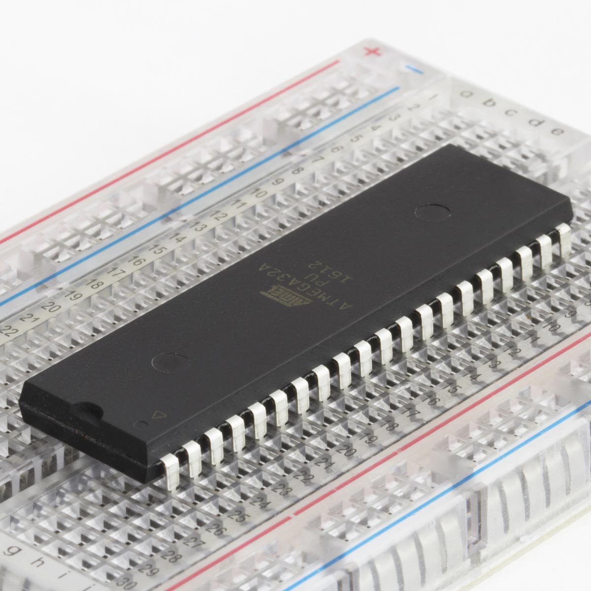
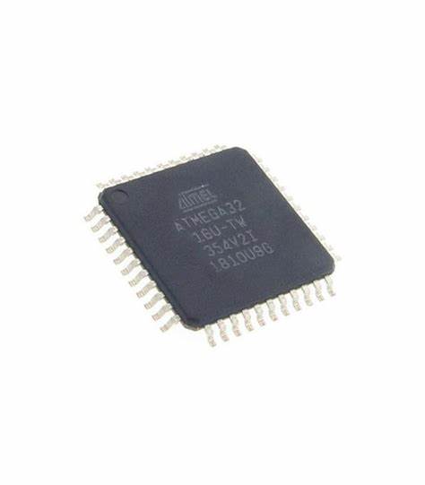
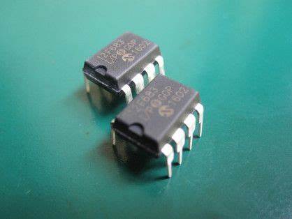
 Reverse ATMEL AVR MCU ATmega32A Heximal Code
Reverse ATMEL AVR MCU ATmega32A Heximal Code is a process to unlock atmega32a locked microcontroller fuse bit and read embedded firmware out from atmega32a avr chip flash memory;
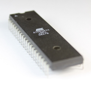
crack avr mcu atmega32a protection and copy heximal file
The AVR Stack Pointer is implemented as two 8-bit registers in the I/O space. The number of bits actually used is implementation dependent. Note that the data space in some implementations of the AVR architecture is so small that only SPL is needed. In this case, the SPH Register will not be present.
This section describes the general access timing concepts for instruction execution. The Atmel®AVR® CPU is driven by the CPU clock clkCPU, directly generated from the selected clock source for the chip. No internal clock division is used.
revertir ATMEL AVR MCU ATmega32A código heximal es un proceso para desbloquear atmega32a microcontrolador bloqueado bit fusible y leer el firmware embebido a cabo a partir de atmega32a avr chip de memoria flash
Figure 5 shows the parallel instruction fetches and instruction executions enabled by the Harvard architecture and the fast-access Register File concept. This is the basic pipe-lining concept to obtain up to 1 MIPS per MHz with the corresponding unique results for functions per cost, functions per clocks, and functions per power-unit to copy avr mcu atmega32a software.
Figure 6 shows the internal timing concept for the Register File. In a single clock cycle an ALU operation using two register operands is executed, and the result is stored back to the destination register.
Reverse ATMEL AVR MCU ATmega32A Heximal Code is a process to unlock atmega32a locked microcontroller fuse bit and read embedded firmware out from atmega32a avr chip flash memory
The Atmel®AVR® provides several different interrupt sources. These interrupts and the separate Reset Vector each have a separate Program Vector in the Program memory space. All interrupts are assigned individual enable bits which must be written logic one together with the Global Interrupt Enable bit in the Status Register in order to enable the interrupt by breaking of avr microcontroller atmega32a protection fuse bit.
Depending on the Program Counter value, interrupts may be automatically disabled when Boot Lock Bits BLB02 or BLB12 are programmed. This feature improves software security. See the section “Memory Programming” on page 215 for details.
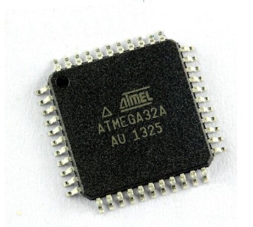
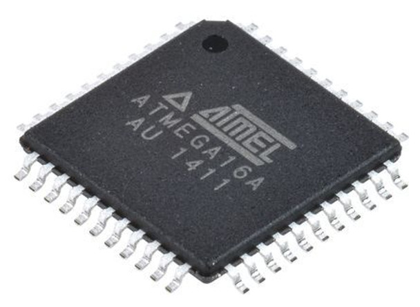
ATMEL AVR Microcontroller ATmega32 Flash Memory Breaking
ATMEL AVR Microcontroller ATmega32 Flash Memory Breaking is a process to clone embedded code from atmega32 mcu flash memory, the firmware of flash memory of avr mcu atmega32 can be readout;
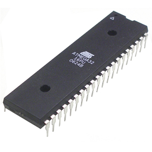
ATMEL AVR Microcontroller ATmega32 Flash Memory Breaking is a process to clone embedded code from atmega32 mcu flash memory, the firmware of flash memory of avr mcu atmega32 can be readout
The Register File is optimized for the AVR Enhanced RISC instruction set. In order to achieve the required performance and flexibility, the following input/output schemes are supported by the Register File:
- One 8-bit output operand and one 8-bit result input
- Two 8-bit output operands and one 8-bit result input
- Two 8-bit output operands and one 16-bit result input
- One 16-bit output operand and one 16-bit result input
Figure 3 shows the structure of the 32 general purpose working registers in the CPU.
Most of the instructions operating on the Register File have direct access to all registers, and most of them are single cycle instructions.
ATMEL AVR microcontrolador ATmega32 romper la memoria flash es un proceso para clonar código embebido de la memoria flash mcu atmega32, el firmware de la memoria flash de avr mcu atmega32 puede ser readout;
As shown in Figure 3, each register is also assigned a Data memory address, mapping them directly into the first 32 locations of the user Data Space. Although not being physically implemented as SRAM locations, this memory organization provides great flexibility in access of the registers to copy avr microcontroller atmega32 flash software, as the X-pointer, Y-pointer, and Z-pointer Registers can be set to index any register in the file.
The registers R26..R31 have some added functions to their general purpose usage. These reg- isters are 16-bit address pointers for indirect addressing of the Data Space. The three indirect address registers X, Y and Z are defined as described in Figure 4.
The Stack is mainly used for storing temporary data, for storing local variables and for storing return addresses after interrupts and subroutine calls. The Stack Pointer Register always points to the top of the Stack. Note that the Stack is implemented as growing from higher memory loca- tions to lower memory locations. This implies that a Stack PUSH command decreases the Stack Pointer.

crack avr atmel microprocessor atmega32 fuse bit and extract embedded code from atmega32 mcu flash memory
The Stack Pointer points to the data SRAM Stack area where the Subroutine and Interrupt Stacks are located. This Stack space in the data SRAM must be defined by the program before any subroutine calls are executed or interrupts are enabled. The Stack Pointer must be set to point above 0x60 by recovering atmega32 microprocessor flash memory content.
The Stack Pointer is decremented by one when data is pushed onto the Stack with the PUSH instruction, and it is decremented by two when the return address is pushed onto the Stack with subroutine call or interrupt. The Stack Pointer is incremented by one when data is popped from the Stack with the POP instruction, and it is incremented by two when address is popped from the Stack with return from subroutine RET or return from interrupt RETI.
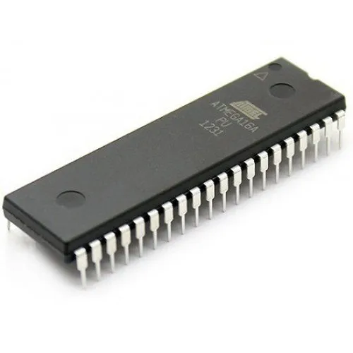
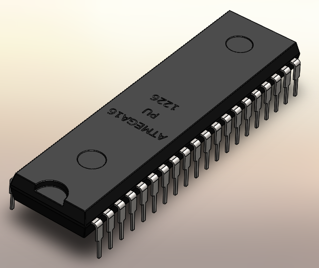
Secured Microcontroller ATmega16A Flash Code Extraction
Secured Microcontroller ATmega16A Flash Code Extraction needs to readout the program software from atmega16a locked mcu after unlock locked microprocessor atmega16a tamper resistance system;
Secured Microcontroller ATmega16A Flash Code Extraction needs to readout the program software from atmega16a locked mcu after unlock locked microprocessor atmega16a tamper resistance system;
When entering Power-down sleep mode while an EEPROM write operation is active, the EEPROM write operation will continue, and will complete before the Write Access time has passed. However, when the write operation is completed, the Oscillator continues running, and as a consequence, the device does not enter Power-down entirely. It is therefore recommended to verify that the EEPROM write operation is completed before entering Power-down.
microcontrolador asegurado ATmega16A flash extracción de código necesita para leer el software del programa de atmega16a bloqueado mcu después de desbloquear microprocesador bloqueado atmega16a sistema de resistencia a la manipulación;
During periods of low VCC, the EEPROM data can be corrupted because the supply voltage is too low for the CPU and the EEPROM to operate properly. These issues are the same as for board level systems using EEPROM, and the same design solutions should be applied.
Защищенный микроконтроллер ATmega16A Извлечение флэш-кода необходимо для считывания программного обеспечения из заблокированного микроконтроллера atmega16a после разблокировки заблокированного микропроцессора atmega16a системы защиты от несанкционированного доступа;
An EEPROM data corruption can be caused by two situations when the voltage is too low. First, a regular write sequence to the EEPROM requires a minimum voltage to operate correctly. Sec- ond, the CPU itself can execute instructions incorrectly, if the supply voltage is too low to readout atmega16a ic chip locked code.
EEPROM data corruption can easily be avoided by following this design recommendation:
Keep the AVR RESET active (low) during periods of insufficient power supply voltage. This can be done by enabling the internal Brown-out Detector (BOD). If the detection level of the internal BOD does not match the needed detection level, an external low VCC Reset Protection circuit can be used. If a reset occurs while a write operation is in progress, the write operation will be completed provided that the power supply voltage is sufficient.
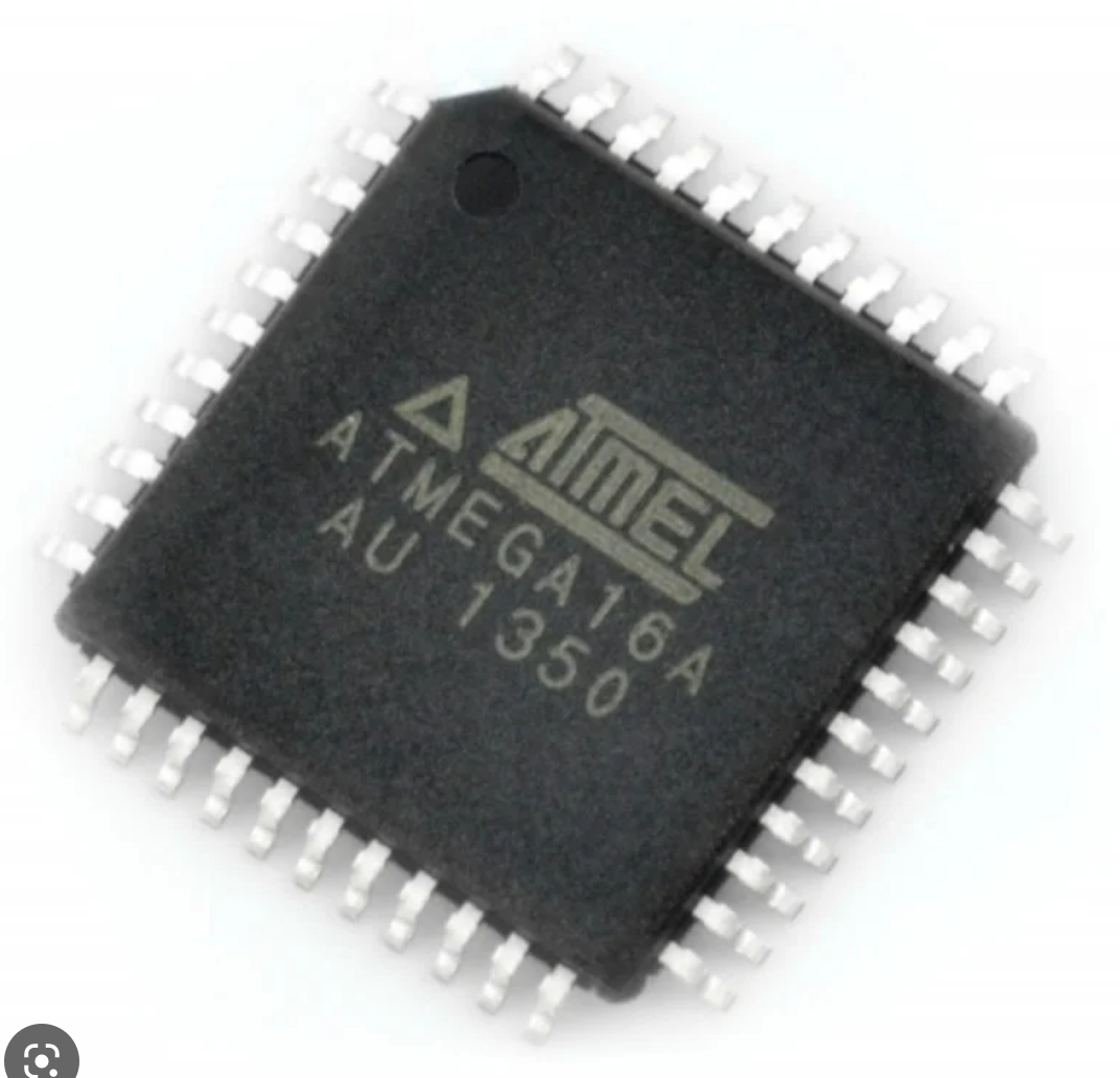
Unlock Encrypted MCU ATmega16 Heximal
Unlock Encrypted MCU ATmega16 Heximal will need engineer to attack atmega16 microcontroller protection system then readout embedded source code from atmega16 microprocessor flash memory;
Unlock Encrypted MCU ATmega16 Heximal will need engineer to attack atmega16 microcontroller protection system then readout embedded source code from atmega16 microprocessor flash memory;
The EEPROM Address Registers – EEARH and EEARL – specify the EEPROM address in the 512bytes EEPROM space. The EEPROM data bytes are addressed linearly between 0 and 511. The initial value of EEAR is undefined. A proper value must be written before the EEPROM may be accessed.
For the EEPROM write operation, the EEDR Register contains the data to be written to the EEPROM in the address given by the EEAR Register. For the EEPROM read operation, the EEDR contains the data read out from the EEPROM at the address given by EEAR.
desbloquear cifrado MCU ATmega16 heximal necesitará ingeniero para atacar atmega16 microcontrolador sistema de protección a continuación, leer código fuente embebido de atmega16 microprocesador de memoria flash
The EEMWE bit determines whether setting EEWE to one causes the EEPROM to be written. When EEMWE is set, setting EEWE within four clock cycles will write data to the EEPROM at the selected address If EEMWE is zero to copying atmega165 mcu firmware, setting EEWE will have no effect. When EEMWE has been written to one by software, hardware clears the bit to zero after four clock cycles.
Unlock Encrypted MCU ATmega16 Heximal will need engineer to attack atmega16 microcontroller protection system then readout embedded source code from atmega16 microprocessor flash memory
The EEPROM Write Enable Signal EEWE is the write strobe to the EEPROM. When address and data are correctly set up, the EEWE bit must be written to one to write the value into the EEPROM. The EEMWE bit must be written to one before a logical one is written to EEWE, otherwise no EEPROM write takes place. The following procedure should be followed when writing the EEPROM (the order of steps 3 and 4 is not essential):
- Wait until EEWE becomes zero
- Wait until SPMEN in SPMCR becomes zero
- Write new EEPROM address to EEAR (optional)
- Write new EEPROM data to EEDR (optional)
- Write a logical one to the EEMWE bit while writing a zero to EEWE in EECR
Within four clock cycles after setting EEMWE, write a logical one to EEWE by breaking atmega16 microcontroller fuse bit;
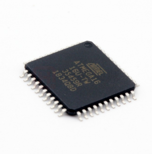
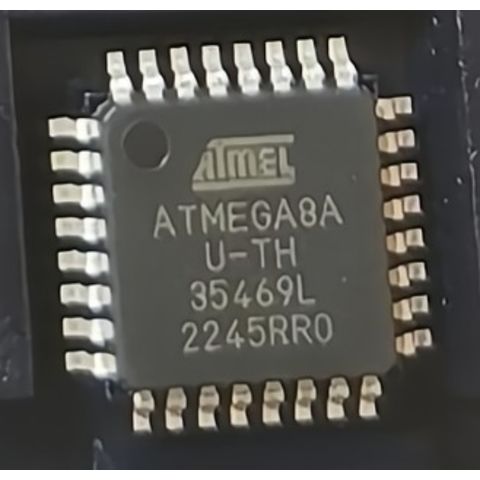
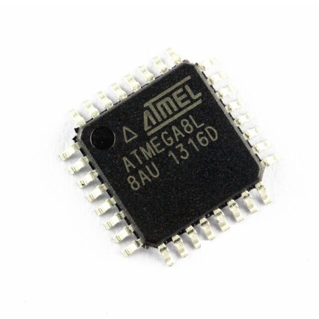
Deciphering AVR MCU ATmega8A Heximal Data
Deciphering AVR MCU ATmega8A Heximal Data from its flash memory needs to decode microprocessor atmega8a security fuse bit then read software file out from atmega8a microcontroller flash memory;
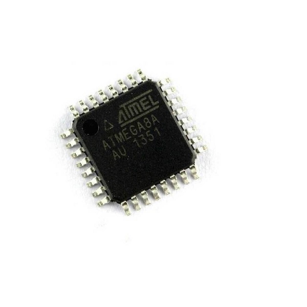
Deciphering AVR MCU ATmega8A Heximal Data from its flash memory needs to decode microprocessor atmega8a security fuse bit then read software file out from atmega8a microcontroller flash memory
Features
· High-performance, Low-power AVR® 8-bit Microcontroller
· Advanced RISC Architecture
– 130 Powerful Instructions – Most Single-clock Cycle Execution
– 32 x 8 General Purpose Working Registers
– Fully Static Operation
– Up to 16 MIPS Throughput at 16 MHz
– On-chip 2-cycle Multiplier
High Endurance Non-volatile Memory segments
– 8K Bytes of In-System Self-programmable Flash program memory
– 512 Bytes EEPROM
– 1K Byte Internal SRAM
– Write/Erase Cycles: 10,000 Flash/100,000 EEPROM
– Data retention: 20 years at 85°C/100 years at 25°C(1)
– Optional Boot Code Section with Independent Lock Bits
· In-System Programming by On-chip Boot Program
· True Read-While-Write Operation
Расшифровка шестнадцатеричных данных AVR MCU ATmega8A из его флэш-памяти требует декодирования бита безопасности микропроцессора atmega8a, а затем считывания файла программного обеспечения из флэш-памяти микроконтроллера atmega8a.
8-bit with 8K Bytes In-System Programmable
– Programming Lock for Software Security
Peripheral Features
– Two 8-bit Timer/Counters with Separate Prescaler, one Compare Mode
– One 16-bit Timer/Counter with Separate Prescaler, Compare Mode, and Capture Mode
– Real Time Counter with Separate Oscillator
– Three PWM Channels
– 8-channel ADC in TQFP and QFN/MLF package
· Eight Channels 10-bit Accuracy
– 6-channel ADC in PDIP package
· Six Channels 10-bit Accuracy
– Byte-oriented Two-wire Serial Interface
– Programmable Serial USART
– Master/Slave SPI Serial Interface
– Programmable Watchdog Timer with Separate On-chip Oscillator
– On-chip Analog Comparator
Special Microcontroller Features
– Power-on Reset and Programmable Brown-out Detection
– Internal Calibrated RC Oscillator
– External and Internal Interrupt Sources
– Five Sleep Modes: Idle, ADC Noise Reduction, Power-save, Power-down, and Standby
I/O and Packages
– 23 Programmable I/O Lines
– 28-lead PDIP, 32-lead TQFP, and 32-pad QFN/MLF
Operating Voltages
– 2.7 – 5.5V for ATmega8A
Speed Grades
– 0 – 16 MHz for ATmega8A
Power Consumption at 4 Mhz, 3V, 25°
descifrar AVR MCU ATmega8A datos heximales de su memoria flash necesita para descifrar microprocesador atmega8a fusible de seguridad de bits a continuación, leer el archivo de software de la memoria flash del microcontrolador atmega8a;
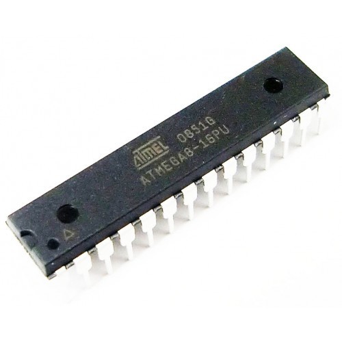
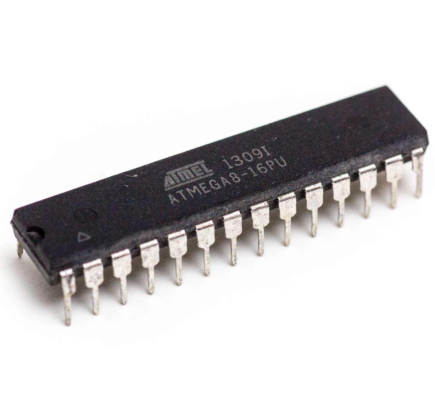
Locked MCU ATmega8L Flash Program Replication
Locked MCU ATmega8L Flash Program Replication needs to break off protective microcontroller atmega8l fuse bit, and then extract firmware from atmega8l microprocessor flash memory;
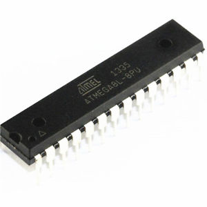
Locked MCU ATmega8L Flash Program Replication needs to break off protective microcontroller atmega8l fuse bit, and then extract firmware from atmega8l microprocessor flash memory;
Depending on the clock selection fuse settings, PB6 can be used as input to the inverting Oscil- lator amplifier and input to the internal clock operating circuit.
Depending on the clock selection fuse settings, PB7 can be used as output from the inverting Oscillator amplifier.
If the Internal Calibrated RC Oscillator is used as chip clock source, PB7..6 is used as TOSC2..1 input for the Asynchronous Timer/Counter2 if the AS2 bit in ASSR is set.
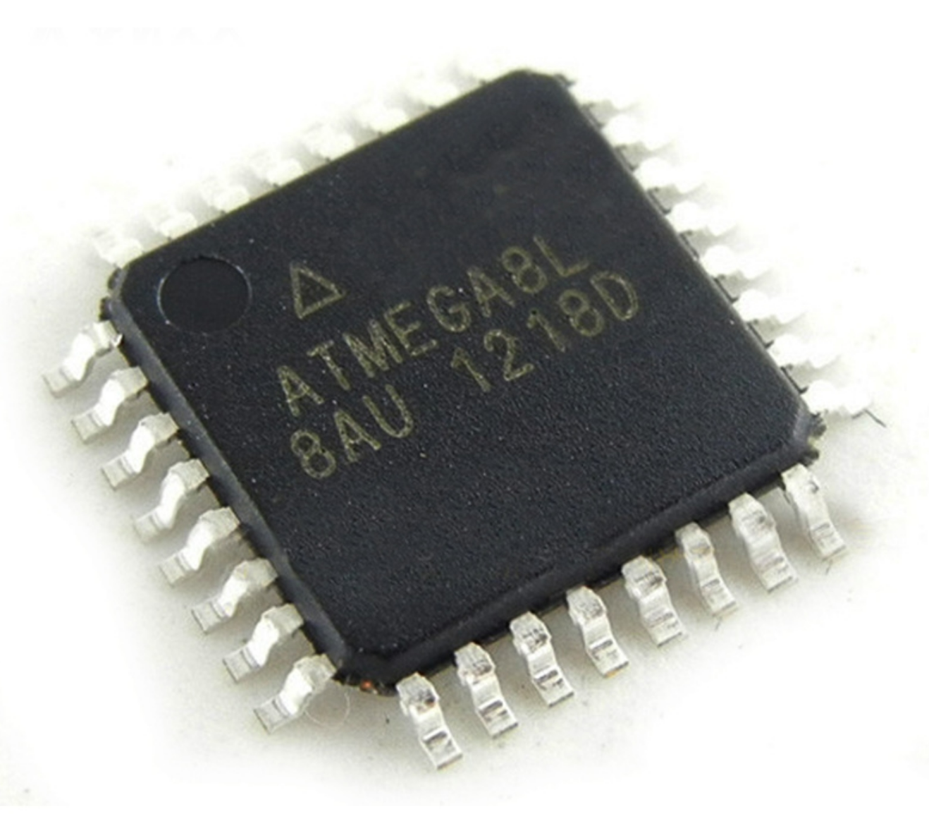
bloqueado MCU ATmega8L flash programa de replicación necesita para romper el microcontrolador protector atmega8l fusible bit, y luego extraer el firmware de la memoria flash del microprocesador atmega8l;
Port C is an 7-bit bi-directional I/O port with internal pull-up resistors (selected for each bit). The Port C output buffers have symmetrical drive characteristics with both high sink and source capability. As inputs, Port C pins that are externally pulled low will source current if the pull-up resistors are activated. The Port C pins are tri-stated when a reset condition becomes active, even if the clock is not running to restore atmega8l microcontroller flash data.
If the RSTDISBL Fuse is programmed, PC6 is used as an I/O pin. Note that the electrical char- acteristics of PC6 differ from those of the other pins of Port C.
hack atmega8l mcu tamper resistance and readout flash program from atmega8l microcontroller
If the RSTDISBL Fuse is unprogrammed, PC6 is used as a Reset input. A low level on this pin for longer than the minimum pulse length will generate a Reset, even if the clock is not running. The minimum pulse length is given in Table 15 on page 38. Shorter pulses are not guaranteed to generate a Reset when copying atmega8l microprocessor flash data.
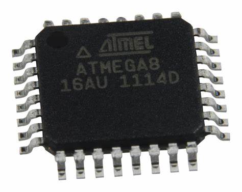
Break ATmega8 Encrypted MCU Fuse Bit
Break ATmega8 Encrypted MCU Fuse Bit by focus ion beam will help engineer to copy avr chip atmega8 microcontroller flash firmware, after extract embedded firmware from microprocessor atmega8 secured flash memory;
Break ATmega8 Encrypted MCU Fuse Bit by focus ion beam will help engineer to copy avr chip atmega8 microcontroller flash firmware, after extract embedded firmware from microprocessor atmega8 secured flash memory
The boot program can use any interface to download the application program in the Application Flash memory. Software in the Boot Flash Section will continue to run while the Application Flash Section is updated, providing true Read-While-Write operation by recovery atmega8 mcu flash memory content. By combining an 8-bit RISC CPU with In-System Self-Programmable Flash on a monolithic chip, the Atmel ATmega8 is a powerful microcontroller that provides a highly-flexible and cost-effective solution to many embedded control applications.
Leer AVR ATMEGA8L Microcontrolador Código Protegido necesita ingeniería inversa atmega8l mcu sistema de resistencia a la manipulación y, a continuación, recuperar el firmware embebido de atmega8l microprocesador de memoria flash;
The ATmega8 is supported with a full suite of program and system development tools, including C compilers, macro assemblers, program simulators, and evaluation kits.
secured atmega8 mcu protection cracking can recover heximal from microcontroller atmega8 flash memory
Typical values contained in this datasheet are based on simulations and characterization of other AVR microcontrollers manufactured on the same process technology. Minimum and Maxi- mum values will be available after the device is characterized.
Port B is an 8-bit bi-directional I/O port with internal pull-up resistors (selected for each bit). The Port B output buffers have symmetrical drive characteristics with both high sink and source capability. As inputs, Port B pins that are externally pulled low will source current if the pull-up resistors are activated. The Port B pins are tri-stated when a reset condition becomes active, even if the clock is not running.
Break Microchip PIC12F752 Locked MCU Flash Memory
Break Microchip PIC12F752 Locked MCU Flash Memory protection over its fuse bit and readout embedded heximal program from PIC12F752 Microcontroller for cloning;
Break Microchip PIC12F752 Locked MCU Flash Memory protection over its fuse bit and readout embedded heximal program from PIC12F752 Microcontroller for cloning;
For oscillator modes involving a crystal or resonator (HS, HSPLL, LP or XT), the situation is somewhat dif- ferent. Since the oscillator may require a start-up time considerably longer than the FCSM sample clock time, a false clock failure may be detected.
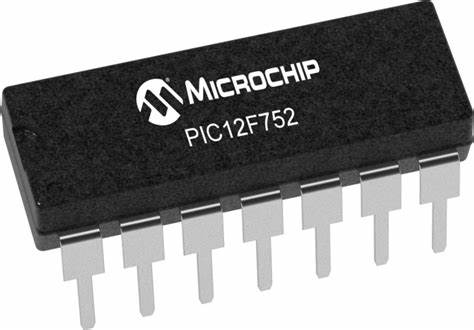
romper microchip PIC12F752 bloqueado MCU protección de memoria flash sobre su bit de fusible y la lectura incrustado programa heximal de PIC12F752 Microcontrolador para la clonación;
To prevent this, the internal oscillator block is automatically configured as the system clock and functions until the primary clock is stable (the OST and PLL timers have timed out) to readout pic12f509 flash memory file. This is identical to Two-Speed Start-up mode. Once the primary clock is stable, the INTRC returns to its role as the FSCM source.
Recover embedded binary file from Microprocessor PIC12F752 flash memory
As noted in Section 19.3.1 “Special Considerations for Using Two-Speed Start-up”, it is also possible to select another clock configuration and enter an alter- nate power managed mode while waiting for the primary system clock to become stable. When the new powered managed mode is selected, the primary clock is disabled.
The same logic that prevents false oscilla- tor failure interrupts on POR or wake from Sleep will also prevent the detection of the oscillator’s failure to start at all following these events. This can be avoided by monitoring the OSTS bit and using a timing routine to determine if the oscillator is taking too long to start. Even so, no oscillator failure interrupt will be flagged.
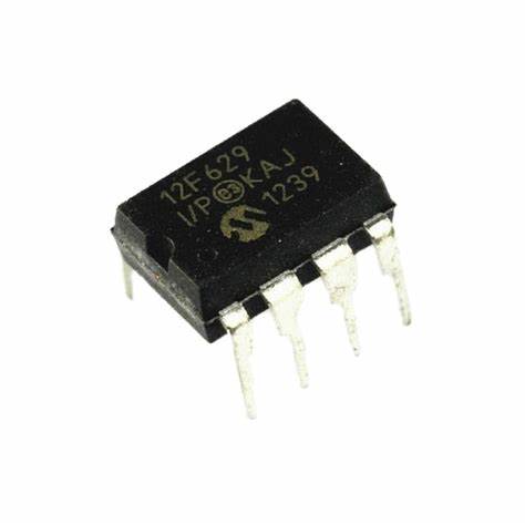
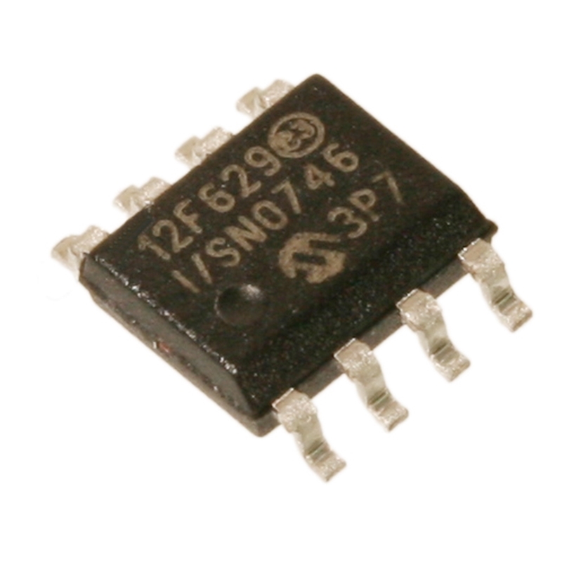
Recover Locked Microcontroller PIC12F629 Flash Data
Recover Locked Microcontroller PIC12F629 Flash Data needs to attack secured MCU PI12F629 protection system and then read out heximal archive file from original microprocessor PIC12F629;
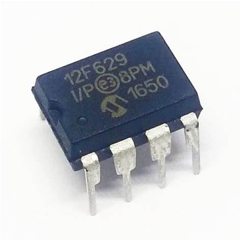
Recuperar microcontrolador bloqueado PIC12F629 Flash Los datos deben descifrar el bit de fusible de seguridad de MCU asegurado PIC12F629 y luego leer el heximal incrustado de la microcomputadora bloqueada PIC12F629
The primary clock source may never become ready during start-up. In this case, operation is clocked by the INTOSC multiplexer. The OSCCON register will remain in its Reset state until a power managed mode is entered.
para recuperar los datos flash del microcontrolador bloqueado PIC12F629 es necesario atacar el sistema de protección del MCU PI12F629 y luego leer el archivo heximal del microprocesador original PIC12F629;
Entering a power managed mode by loading the OSCCON register and executing a SLEEP instruction will clear the Fail-Safe condition to clone microchip pic12f510 microcontroller flash program. When the Fail-Safe condition is cleared, the clock monitor will resume monitoring the peripheral clock.
Kilitli Mikrodenetleyiciyi Kurtar PIC12F629 Flash Verilerinin güvenli MCU PI12F629 koruma sistemine saldırması ve ardından orijinal mikroişlemci PIC12F629’dan onaltılık arşiv dosyasını okuması gerekir
As previously mentioned, entering a power managed mode clears the Fail-Safe condition. By entering a power managed mode, the clock multiplexer selects the clock source selected by the OSCCON register to read microcontroller pic12f509 flash heximal. Fail-Safe monitoring of the power managed clock source resumes in the power managed mode.
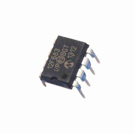
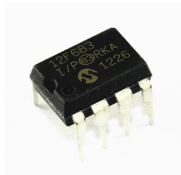
Secured PIC12F683 Microprocessor Heximal Code Recovery
Secured PIC12F683 Microprocessor Heximal Code Recovery is a process to break pic12f683 mcu security fuse bit then read the embedded firmware out from microcontroller pic12f683;
Secured PIC12F683 Microprocessor Heximal Code Recovery è un processo per rompere il bit del fusibile di sicurezza mcu pic12f683, quindi leggere il firmware incorporato dal microcontrollore pic12f683
Clock failure is tested for on the falling edge of the sample clock. If a sample clock falling edge occurs while CM is still set, a clock failure has been detected. This causes the following:
- the FSCM generates an oscillator fail interrupt by setting bit, OSCFIF (PIR2<7>);
- the system clock source is switched to the internal oscillator block (OSCCON is not updated to show the current clock source – this is the Fail-Safe condition); and
- the WDT is
asegurado PIC12F683 microprocesador de recuperación de código heximal es un proceso para romper pic12f683 mcu fusible de seguridad de bits a continuación, leer el firmware embebido a cabo desde el microcontrolador pic12f683;
Since the postscaler frequency from the internal oscil- lator block may not be sufficiently stable, it may be desirable to select another clock configuration and enter an alternate power managed mode when breaking PIC18F242 MCU flash memory (see Section 19.3.1 “Special Considerations for Using Two-Speed Start-up” and Section 3.1.3 “Multiple Sleep Commands” for more details). This can be done to attempt a partial recovery, or execute a controlled shutdown.
Güvenli PIC12F683 Mikroişlemci Onaltılı Kod Kurtarma, pic12f683 mcu güvenlik sigorta bitini kırmak ve ardından gömülü bellenimi mikrodenetleyiciden okumak için bir süreçtir pic12f683
To use a higher clock speed on wake-up, the INTOSC or postscaler clock sources can be selected to provide a higher clock speed by setting bits, IFRC2:IFRC0 when PIC18F252 microcontroller flash memory program recovery, immediately after Reset. For wake-ups from Sleep, the INTOSC or postscaler clock sources can be selected by setting IFRC2:IFRC0 prior to entering Sleep mode.