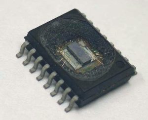
 Recover MCU PIC16F818 Binary
Recover MCU PIC16F818 Binary
LOW POWER FEATURES of PIC16F818 can greatly help hacker to Recover MCU PIC16F818 Binary from its memory:
Power-Managed modes:
– Primary Run: XT, RC oscillator, 87 µA, 1 MHz, 2V
– INTRC: 7 µA, 31.25 kHz, 2V
– Sleep: 0.2 µA, 2V
· Timer1 oscillator: 1.8 µA, 32 kHz, 2V
· Watchdog Timer: 0.7 µA, 2V
· Wide operating voltage range:
– Industrial: 2.0V to 5.5V
Oscillators:
· Three Crystal modes:
– LP, XT, HS: up to 20 MHz
· Two External RC modes
· One External Clock mode:
– ECIO: up to 20 MHz
· Internal oscillator block:
– 8 user selectable frequencies: 31 kHz, 125 kHz,
250 kHz, 500 kHz, 1 MHz, 2 MHz, 4 MHz, 8 MHz
Special Microcontroller Features:
· 100,000 erase/write cycles Enhanced Flash program memory typical
· 1,000,000 typical erase/write cycles EEPROM data memory typical
· EEPROM Data Retention: > 40 years
· In-Circuit Serial ProgrammingTM (ICSPTM) via two pins
· Processor read/write access to program memory
· Low-Voltage Programming
· In-Circuit Debugging via two pins
Peripheral Features:
16 I/O pins with individual direction control
High sink/source current: 25 mA
Timer0: 8-bit timer/counter with 8-bit prescaler
Timer1: 16-bit timer/counter with prescaler, can be
incremented during Sleep via external crystal/clock
Timer2: 8-bit timer/counter with 8-bit period register, prescaler and postscaler
Capture, Compare, PWM (CCP) module:
– Capture is 16-bit, max. resolution is 12.5 ns
– Compare is 16-bit, max. resolution is 200 ns
– PWM max. resolution is 10-bit
10-bit, 5-channel Analog-to-Digital converter
Synchronous Serial Port (SSP) with
SPI™ (Master/Slave) and I2C™ (Slave).
Recover MCU PIC16F628A Binary
Recover MCU PIC16F628A Binary
General Description of PIC16F628A Microcontroller to better understand the process of Recover MCU PIC16F628A Binary:
The PIC16F628A are 18-Pin FLASH based members of the versatile PIC16CXX family of low cost, high performance, CMOS, fully-static, 8-bit microcontrollers
All PICmicro® microcontrollers employ an advanced RISC architecture. The PIC16F628A have enhanced core features, eight-level deep stack, and multiple internal and external interrupt sources. The separate instruction and data buses of the Harvard architecture allow a 14-bit wide instruction word with the separate 8-bit wide data.
The two-stage instruction pipeline allows all instructions to execute in a single cycle, except for program branches (which require two cycles). A total of 35 instructions (reduced instruction set) are available, complemented by a large register set.
PIC16F628A microcontrollers typically achieve a 2:1 code compression and a 4:1 speed improvement over other 8-bit microcontrollers in their class.
PIC16F628A devices have integrated features
The PIC16F628A has 8 oscillator configurations. The single-pin RC oscillator provides a low cost solution. The LP oscillator minimizes power consumption, XT is a standard crystal, and INTOSC is a self contained precision two-speed internal oscillator.
RISC architecture. The PIC16F628A have enhanced core features, eight-level deep stack, and multiple internal and external interrupt sources. The separate instruction and data buses of the Harvard architecture allow a 14-bit wide instruction word with the separate 8-bit wide data. The two-stage instruction pipeline allows all instructions to execute in a single-cycle, except for program branches (which require two cycles). A total of 35 instructions (reduced instruction set) are available, complemented by a large register set
PIC16F628A microcontrollers typically achieve a 2:1 code compression and a 4:1 speed improvement over other 8-bit microcontrollers in their class.
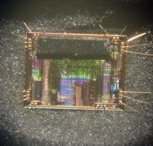
Recover MCU PIC16F627A Dump
Recover MCU PIC16F627A Dump
Unstand the CPU structure can help us better and faster Recover MCU PIC16F627A Dump from its memory:
High Performance RISC CPU:
Operating speeds from DC – 20 MHz when recover mcu
Interrupt capability
8-level deep hardware stack
Direct, Indirect and Relative Addressing modes 35 single word instructions
– All instructions single cycle except branches Special Microcontroller Features:
· Internal and external oscillator options
– Precision Internal 4 MHz oscillator factory calibrated to ±1%
– Low Power Internal 37 kHz oscillator
– External Oscillator support for crystals and resonators
· Power saving SLEEP mode
· Programmable weak pull-ups on PORTB
· Multiplexed Master Clear/Input-pin
· Watchdog Timer with independent oscillator for reliable operation
· Low voltage programming
· In-Circuit Serial Programming™ (via two pins)
· Programmable code protection
· Brown-out Reset
· Power-on Reset if recover mcu
· Power-up Timer and Oscillator Start-up Timer
· Wide operating voltage range. (2.0 – 5.5V)
· Industrial and extended temperature range
· High Endurance FLASH/EEPROM Cell
– 100,000 write FLASH endurance
– 1,000,000 write EEPROM endurance
– 100 year data retention
Low Power Features:
· Standby Current:
– 100 nA @ 2.0V, typical
· Operating Current:
– 12 µA @ 32 kHz, 2.0V, typical
– 120 µA @ 1 MHz, 2.0V, typical
· Watchdog Timer Current
– 1 µA @ 2.0V, typical
· Timer1 oscillator current:
– 1.2 µA @ 32 kHz, 2.0V, typical
· Dual Speed Internal Oscillator:
– Run-time selectable between 4 MHz and 37 kHz
– 4 µs wake-up from SLEEP, 3.0V
Peripheral Features:
· 16 I/O pins with individual direction control
· High current sink/source for direct LED drive
· Analog comparator module with:
– Two analog comparators
– Programmable on-chip voltage reference (VREF) module
– Selectable internal or external reference
– Comparator outputs are externally accessible
· Timer0: 8-bit timer/counter with 8-bit programmable prescaler
· Timer1: 16-bit timer/counter with external crystal/clock capability
· Timer2: 8-bit timer/counter with 8-bit period register, prescaler and postscaler
· Capture, Compare, PWM module
– 16-bit Capture/Compare
– 10-bit PWM
· Addressable Universal Synchronous/Asynchronous Receiver/Transmitter USART/SCI
Recover MCU PIC16F716 Eeprom
Recover MCU PIC16F716 Eeprom
Recover MCU PIC16F716 Eeprom and flash content from memory needs to know the features of the core:
Microcontroller Core Features:
· High-performance RISC CPU
· Only 35 single-word instructions to learn
– All single-cycle instructions except for program branches which are two-cycle
· Operating speed: DC – 20 MHz clock input DC – 200 ns instruction cycle
· Interrupt capability (up to 7 internal/external interrupt sources)
· 8-level deep hardware stack
· Direct, Indirect and Relative Addressing modes
Special Microcontroller Features
· Power-on Reset (POR)
· Power-up Timer (PWRT) and Oscillator Start-up Timer (OST)
· Watchdog Timer (WDT) with its own on-chip RC oscillator for reliable operation
· Dual level Brown-out Reset circuitry
– 2.5 VBOR (Typical)
– 4.0 VBOR (Typical)
Recover MCU PIC16F716 Eeprom
· Programmable code protection
· Power saving Sleep mode
· Selectable oscillator options
· Fully static design
· In-Circuit Serial Programming (ICSP™)
CMOS Technology
· Wide operating voltage range:
– Industrial: 2.0V to 5.5V
– Extended: 3.0V to 5.5V
· High Sink/Source Current 25/25 mA
· Wide temperature range
– Industrial: -40°C to 85°C
– Extended: -40°C to 125°C
Low-Power Features:
· Standby Current:
– 100 nA @ 2.0V, typical
· Operating Current:
– 14 µA @ 32 kHz, 2.0V, typical
– 120 µA @ 1 MHz, 2.0V, typical
· Watchdog Timer Circuit:
– 1 µA @ 2.0V, typical
· Timer1 Oscillator Current:
– 3.0 µA @ 32 kHz, 2.0V
Peripheral Features:
· Timer0: 8-bit timer/counter with 8-bit prescaler
· Timer1: 16-bit timer/counter with prescaler can be incremented during Sleep via external crystal/clock
· Timer2: 8-bit timer/counter with 8-bit period register, prescaler and postscaler
· Enhanced Capture, Compare, PWM module:
– Capture is 16-bit, max. resolution is 12.5 ns
– Compare is 16-bit, max. resolution is 200 ns
– PWM maximum resolution is 10-bit
– Enhanced PWM:
– Single, Half-Bridge and Full-Bridge modes
– Digitally programmable dead-band delay
– Auto-shutdown/restart
· 8-bit multi-channel Analog-to-Digital converter
· 13 I/O pins with individual direction control
· Programmable weak pull-ups on PORTB
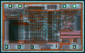
Recover MCU PIC16F76 Heximal
Recover MCU PIC16F76 Heximal
Recover MCU PIC16F76 Heximal from its memory which include the eeprom and flash part:
This document contains device specific information about the following devices PIC16F76,
PIC16F76 devices are available only in 28-pin packages, while PIC16F77 devices are available in 40-pin and 44-pin packages. All devices in the PIC16F7X family share common architecture, with the following differences when recover mcu:
· The PIC16F73 and PIC16F76 have one-half of the total on-chip memory of the PIC16F74 and PIC16F77
· The 28-pin devices have 3 I/O ports, while the 40/44-pin devices have 5
· The 28-pin devices have 11 interrupts, while the 40/44-pin devices have 12
· The 28-pin devices have 5 A/D input channels, while the 40/44-pin devices have 8
· The Parallel Slave Port is implemented only on the 40/44-pin devices after recover mcu:
The available features are summarized in Table 1-1.
Block diagrams of the PIC16F73/76 and PIC16F74/77
Additional information may be found in the PICmicro™ Mid-Range Reference Manual (DS33023), which may be obtained from your local Microchip Sales Representative or downloaded from the Microchip website. The Reference Manual should be considered a complementary document to this data sheet, and is highly recommended reading for a better understanding of the device architecture and operation of the peripheral modules.
MEMORY ORGANIZATION:
There are two memory blocks in each of these PICmicro® MCUs. The Program Memory and Data Memory have separate buses so that concurrent access can occur and is detailed in this section. The Program Memory can be read internally by user code
Additional information on device memory may be found in the PICmicro Mid-Range Reference Manual (DS33023). e’>· The 28-pin devices have 11 interrupts, while the 40/44-pin devices have 12
· The 28-pin devices have 5 A/D input channels, while the 40/44-pin devices have 8
· The Parallel Slave Port is implemented only on the 40/44-pin devices
Recover MCU PIC16F72 Code
Recover MCU PIC16F72 Code
Recover MCU PIC16F72 Code from both its eeprom and flash, below pls check its features:
High Performance RISC CPU:
· Only 35 single word instructions to learn
· All single cycle instructions except for program branches, which are two-cycle after recover MCU code
· Operating speed: DC – 20 MHz clock input DC – 200 ns instruction cycle
· 2K x 14 words of Program Memory, 128 x 8 bytes of Data Memory (RAM)
· Pinout compatible to PIC16C72/72A and PIC16F872
· Interrupt capability if recover MCU code
· Eight-level deep hardware stack
· Direct, Indirect and Relative Addressing modes
Peripheral Features:
· High Sink/Source Current: 25 mA
· Timer0: 8-bit timer/counter with 8-bit prescaler
· Timer1: 16-bit timer/counter with prescaler, can be incremented during SLEEP via external crystal/clock
· Timer2: 8-bit timer/counter with 8-bit period register, prescaler and postscaler
· Capture, Compare, PWM (CCP) module when recover MCU code
– Capture is 16-bit, max. resolution is 12.5 ns
– Compare is 16-bit, max. resolution is 200 ns
– PWM max. resolution is 10-bit
· 8-bit, 5-channel analog-to-digital converter
· Synchronous Serial Port (SSP) with SPI™ (Master/Slave) and I2C™ (Slave)
· Brown-out detection circuitry for Brown-out Reset (BOR)
CMOS Technology:
Low power, high speed CMOS FLASH technology
Fully static design for the purpose of recover MCU code
Wide operating voltage range: 2.0V to 5.5V
Industrial temperature range
Low power consumption:
Special Microcontroller Features:
· 1,000 erase/write cycle FLASH program memory typical
· Power-on Reset (POR), Power-up Timer (PWRT) and Oscillator Start-up Timer (OST)
· Watchdog Timer (WDT) with its own on-chip RC oscillator for reliable operation
· Programmable code protection
· Power saving SLEEP mode
Selectable oscillator options
· In-Circuit Serial Programming™ (ICSP™) via 2 pins
· Processor read access to program memory
RC oscillator for reliable operation
· Programmable code protection
· Power saving SLEEP mode
Recover PIC MCU Microchip 16LF506 Firmware
Recover PIC MCU Microchip PIC16LF506 Firmware
Data memory is composed of registers or bytes of RAM. Therefore, data memory for a device is specified by its register file from Recover PIC MCU Microchip PIC16LF506 Firmware. The register file is divided into two functional groups: Special Function Registers (SFR) and General Purpose Registers (GPR).
The Special Function Registers include the TMR0 register, the Program Counter (PCL), the STATUS register, the I/O registers (ports) and the File Select Register (FSR). In addition, Special Function Registers are used to control the I/O port configuration and prescaler options.
Recover PIC MCU Microchip PIC16LF506 Firmware
The General Purpose Registers are used for data and control information under command of the instructions. For the PIC12F510, the register file is composed of 10 Special Function Registers, 6 General Purpose.
Registers and 32 General Purpose Registers accessed For the PIC16F506, the register file is composed of 13 Special Function Registers, 3 General Purpose Registers and 64 General Purpose Registers accessed from MCU CRACK.
The Special Function Registers (SFRs) are registers used by the CPU and peripheral functions to control the operation of the device. The Special Function Registers can be classified into two sets. The Special Function Registers associated with the “core” functions are described in this section.
Those related to the operation of the peripheral features are described in the section for each peripheral feature. This register contains the arithmetic status of the ALU, the Reset status and the page preselect bit.
The STATUS register can be the destination for any instruction, as with any other register. If the STATUS register is the destination for an instruction that affects the Z, DC or C bits, then the write to these three bits is disabled. These bits are set or cleared according to the device logic. Furthermore, the TO and PD bits are not writable. Therefore, the result of an instruction with the STATUS register as destination may be different than intended.
For example, CLRF STATUS, will clear the upper three bits and set the Z bit. This leaves the STATUS register
as 000u u1uu (where u = unchanged).
Therefore, it is recommended that only BCF, BSF and MOVWF instructions be used to alter the STATUS register. These instructions do not affect the Z, DC or C bits from the STATUS register. For other instructions which do affect Status bits.
Recover PIC MCU Microchip 12F510 Firmware
Recover PIC MCU Microchip 12F510 Firmware
The PIC12F510 devices from Microchip Technology are low-cost, high-performance, 8-bit, fully static, Flash-based CMOS microcontrollers. They employ a RISC architecture with only 33 single-word/ single-cycle instructions. All instructions are single cycle except for program branches, which take two cycles. The PIC12F510 devices deliver performance in an order of magnitude higher than their competitors in the same price category to Recover PIC MCU Microchip 12F510 Firmware.
The 12-bit wide instructions are highly symmetrical, resulting in a typical 2:1 code compression over other 8-bit microcontrollers in its class. The easy-to-use and easy-to-remember instruction set reduces development time significantly.
The PIC12F510/16F506 products are equipped with special features that reduce system cost and power requirements. The Power-on Reset (POR) and Device Reset Timer (DRT) eliminate the need for external Reset circuitry. There are four oscillator configurations to choose from (six on the PIC16F506), including INTOSC Internal Oscillator mode and the power-saving LP (Low-power) Oscillator mode. Power-saving Sleep mode, Watchdog Timer and code protection features improve system cost, power and reliability.
The PIC12F510/16F506 devices allow the customer to take full advantage of Microchip’s price leadership in Flash programmable microcontrollers, while benefiting from the Flash programmable flexibility.
The PIC12F510/16F506 products are supported by a full-featured macro assembler, a software simulator, an in-circuit emulator, a ‘C’ compiler, a low-cost development programmer and a full featured programmer. All the tools are supported on IBM® PC and compatible machines.
Recover PIC MCU Microchip 12F510 Firmware
APPLICATION:
The PIC12F510/16F506 devices fit in applications ranging from personal care appliances and security systems to low-power remote transmitters/receivers. The Flash technology makes customizing application programs (transmitter codes, appliance settings, receiver frequencies, etc.) extremely fast and convenient.
The small footprint packages, for through hole or surface mounting, make these microcontrollers perfect for applications with space limitations. Low-cost, low-power, high-performance, ease-of-use and I/O flexibility make the PIC12F510/16F506 devices very versatile, even in areas where no microcontroller use has been considered before (e.g., timer functions, logic and PLDs in larger systems and coprocessor applications).
Break MCU PIC16F946 Program
Break MCU PIC16F946 Program
AUSART Operation During Sleep can help to Break MCU PIC16F946 Program
The AUSART will remain active during Sleep only in the Synchronous Slave mode. All other modes require the system clock and therefore cannot generate the necessary signals to run the Transmit or Receive Shift registers during Sleep.
Synchronous Slave mode uses an externally generated clock to run the Transmit and Receive Shift registers.
9.4.1 SYNCHRONOUS RECEIVE DURING SLEEP
To receive during Sleep, all the following conditions must be met before entering Sleep mode:
· RCSTA and TXSTA Control registers must be configured for Synchronous Slave Reception.
· If interrupts are desired, set the RCIE bit of the PIE1 register and the PEIE bit of the INTCON register.
Upon entering Sleep mode, the device will be breaky to accept data and clocks on the RX/DT and TX/CK pins, respectively. When the data word has been completely clocked in by the external device, the RCIF interrupt flag bit of the PIR1 register will be set. Thereby, waking the processor from Sleep.
Break MCU PIC16F946 Program
Upon waking from Sleep, the instruction following the SLEEP instruction will be executed. If the GIE global interrupt enable bit of the INTCON register is also set, then the Interrupt Service Routine at address 004h will be called.
9.4.2 SYNCHRONOUS TRANSMIT DURING SLEEP
To transmit during Sleep, all the following conditions must be met before entering Sleep mode:
· RCSTA and TXSTA Control registers must be configured for Synchronous Slave Transmission (see Section 9.3.2.2 “Synchronous Slave Transmission Set-up:”).
· The TXIF interrupt flag must be cleared by writing the output data to the TXREG, thereby filling the TSR and transmit buffer from Break MCU PIC16F946 Program.
If interrupts are desired, set the TXIE bit of the PIE1 register and the PEIE bit of the INTCON register.
Upon entering Sleep mode, the device will be breaky to accept clocks on TX/CK pin and transmit data on the RX/DT pin. When the data word in the TSR has been completely clocked out by the external device, the pending byte in the TXREG will transfer to the TSR and the TXIF flag will be set. Thereby, waking the processor from Sleep. At this point, the TXREG is available to accept another character for transmission, which will clear the TXIF flag.
Upon waking from Sleep, the instruction following the SLEEP instruction will be executed. If the GIE global interrupt enable bit is also set then the Interrupt Service Routine at address 0004h after CRACK MCU.
Copy Microcontroller PIC16F737 Flash
Copy Microcontroller PIC16F737 Flash
Copy Microcontroller PIC16F737 Flash starts from knowing its basic features, below we will introduce it:
Low-Power Features:
· Power-Managed modes:
– Primary Run (XT, RC oscillator, 76 µA, 1 MHz, 2V)
– RC_RUN (7 µA, 31.25 kHz, 2V)
– SEC_RUN (9 µA, 32 kHz, 2V)
– Sleep (0.1 µA, 2V)
· Timer1 Oscillator (1.8 µA, 32 kHz, 2V)
· Watchdog Timer (0.7 µA, 2V)
· Two-Speed Oscillator Start-up Oscillators:
Copy Microcontroller PIC16F737 Flash
· Three Crystal modes:
– LP, XT, HS (up to 20 MHz)
· Two External RC modes
– ECIO (up to 20 MHz)
· Internal Oscillator Block:
– 8 user-selectable frequencies (31 kHz, 125 kHz, 250 kHz, 500 kHz, 1 MHz, 2 MHz, 4 MHz, 8 MHz) after Copy Microcontroller
Analog Features:
· 10-bit, up to 14-channel Analog-to-Digital Converter:
– Programmable Acquisition Time
– Conversion available during Sleep mode
· Dual Analog Comparators
· Programmable Low-Current Brown-out Reset (BOR) Circuitry and Programmable Low-Voltage Detect (LVD) A, 32 kHz, 2V) if Unlock Microcontroller
– Sleep (0.1 µA, 2V)
· Timer1 Oscillator (1.8 µA, 32 kHz, 2V)
· Watchdog Timer (0.7 µA, 2V)
· Two-Speed Oscillator Start-up Oscillators:
· Three Crystal modes:
– LP, XT, HS (up to 20 MHz)
· Two External RC modes
– ECIO (up to 20 MHz)
· Internal Oscillator Block:
– 8 user-selectable frequencies (31 kHz, 125 kHz, 250 kHz, 500 kHz, 1 MHz, 2 MHz, 4 MHz, 8 MHz).