Restore Texas Instrument MSP430G2001 Microcontroller Heximal Program
 October 6th, 2020 |
  Author:
 Restore Texas Instrument MSP430G2001 Microcontroller Heximal Program from embedded flash memory after crack microcontroller msp430g2001 security fuse bit and extract IC code;
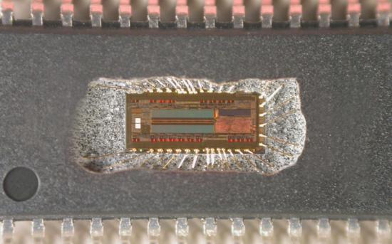
The MSP430 CPU has a 16-bit RISC architecture that is highly transparent to the application. All operations, other than program-flow instructions, are performed as register operations in conjunction with seven addressing modes for source operand and four addressing modes for destination operand.
The CPU is integrated with 16 registers that provide reduced instruction execution time. The register-to-register operation execution time is one cycle of the CPU clock.
Four of the registers, R0 to R3, are dedicated as program counter, stack pointer, status register, and constant generator, respectively. The remaining registers are general-purpose registers.
Peripherals are connected to the CPU using data, address, and control buses, and can be handled with all instructions. The instruction set consists of the original 51 instructions with three formats and seven address modes and additional instructions for the expanded address range. Each instruction can operate on word and byte data to increase the success rate of msp430g2452 microcontroller flash memory protection breaking.
Replicate ARM MCU STM32F105R8T6 Embedded Flash Program
Replicate ARM MCU STM32F105R8T6 Embedded Flash Program and crack arm mcu protective fuse bit and then extract firmware from flash and eeprom memory of microprocessor;
The ARM Cortex™-M3 processor is the latest generation of ARM processors for embedded systems. It has been developed to provide a low-cost platform that meets the needs of MCU implementation, with a reduced pin count and low-power consumption, while delivering outstanding computational performance and an advanced system response to interrupts of arm microcontroller stm32f105vct flash memory content decrypting.
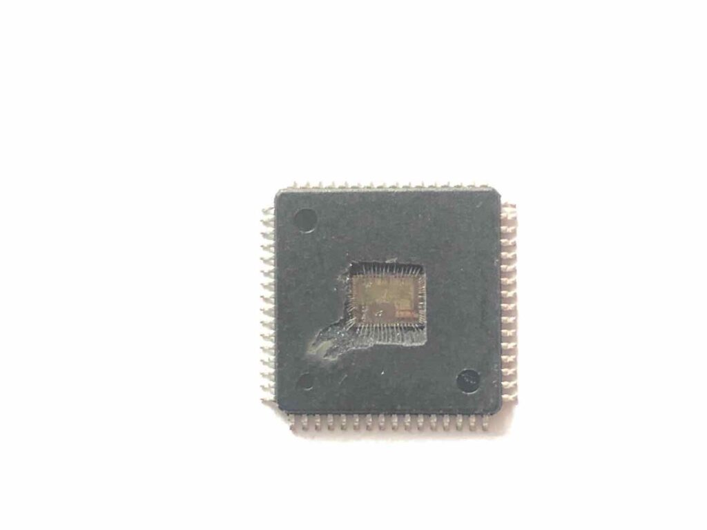
The ARM Cortex™-M3 32-bit RISC processor features exceptional code-efficiency, delivering the high-performance expected from an ARM core in the memory size usually associated with 8- and 16-bit devices.
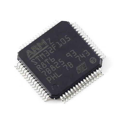
extract arm microprocessor stm32f105r8 source code from flash memory
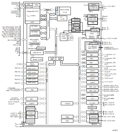
With its embedded ARM core, STM32F105xx and STM32F107xx connectivity line family is compatible with all ARM tools and software. below Figure shows the general block diagram of the device family.
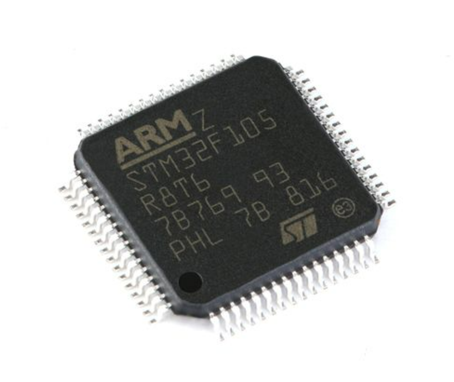
répliquer le programme flash intégré du MCU ARM STM32F105R8T6 et le bit de fusible de protection du MCU Crack Arm, puis extraire le micrologiciel de la mémoire flash et de la mémoire eeprom du microprocesseur ;
Decrypt ARM Microcontroller STM32F105VCT Secured Memory Binary Program
Decrypt ARM Microcontroller STM32F105VCT Secured Memory Binary Program is a process to unlock mcu stm32f105vct tamper resistance system, and then copy firmware from microprocessor;
Features
Core: ARM 32-bit Cortex™-M3 CPU
– 72 MHz maximum frequency, 1.25 DMIPS/MHz (Dhrystone 2.1) performance at 0 wait state memory
LQFP100 14 × 14 mm
LQFP64 10 × 10 mm access
– Single-cycle multiplication and hardware division Memories
– 64 to 256 Kbytes of Flash memory
– up to 64 Kbytes of general-purpose SRAM
Clock, reset and supply management
– 2.0 to 3.6 V application supply and I/Os
– POR, PDR, and programmable voltage detector (PVD)
– 3-to-25 MHz crystal oscillator
– Internal 8 MHz factory-trimmed RC
– Internal 40 kHz RC with calibration
– 32 kHz oscillator for RTC with calibration Low power
– Sleep, Stop and Standby modes
– VBAT supply for RTC and backup registers 2 × 12-bit, 1 µs A/D converters (16 channels)
– Conversion range: 0 to 3.6 V
– Sample and hold capability
– Temperature sensor
– up to 2 MSPS in interleaved mode 2 × 12-bit D/A converters
DMA: 12-channel DMA controller
– Supported peripherals: timers, ADCs, DAC, I2Ss, SPIs, I2Cs and USARTs
Up to 10 timers with pinout remap capability
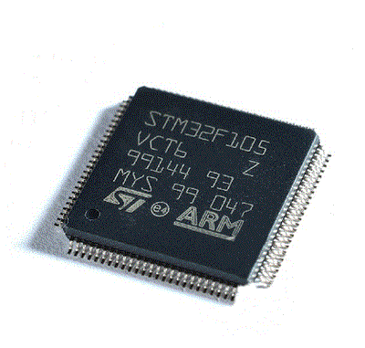
descifrar el microcontrolador ARM STM32F105VCT6 programa binario de memoria segura es un proceso para desbloquear el sistema de resistencia a manipulaciones MCU STM32F105VCT y luego copiar el firmware del microprocesador;
– Up to four 16-bit timers, each with up to 4 IC/OC/PWM or pulse counter and quadrature (incremental) encoder input
– 1 × 16-bit motor control PWM timer with dead-time generation and emergency stop
– 2 × watchdog timers (Independent and Window)
– SysTick timer: a 24-bit downcounter
– 2 × 16-bit basic timers to drive the DAC
Up to 14 communication interfaces with pinout remap capability
– Up to 2 × I2C interfaces (SMBus/PMBus)
– Up to 5 USARTs (ISO 7816 interface, LIN,
IrDA capability, modem control)
– Up to 3 SPIs (18 Mbit/s), 2 with a multiplexed I2S interface that offers audio class accuracy via advanced PLL schemes
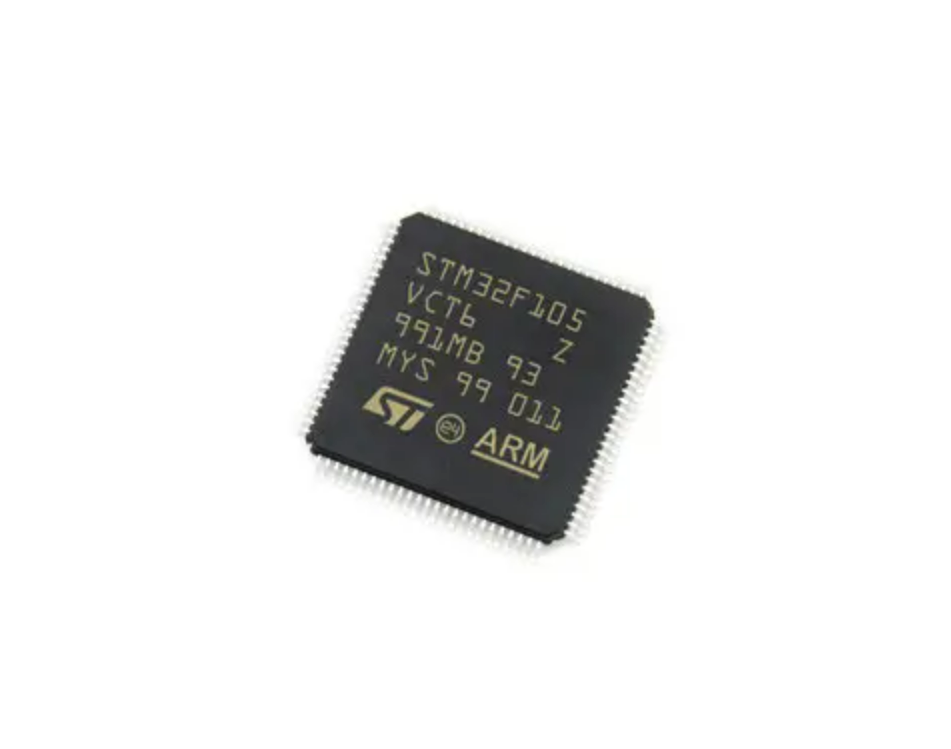
décrypter le microcontrôleur ARM STM32F105VCT6 programme binaire de mémoire sécurisée est un processus permettant de déverrouiller le système de résistance à l’effraction MCU STM32F105VCT, puis de copier le micrologiciel du microprocesseur ;
– 2 × CAN interfaces (2.0B Active) with 512 bytes of dedicated SRAM
– USB 2.0 full-speed device/host/OTG controller with on-chip PHY that supports HNP/SRP/ID with 1.25 Kbytes of dedicated SRAM
– 10/100 Ethernet MAC with dedicated DMA and SRAM (4 Kbytes): IEEE1588 hardware support, MII/RMII available on all packages
– Serial wire debug (SWD) & JTAG interfaces
Restore Microcontroller STM32F103C8 Flash Program Code
Restore Microcontroller STM32F103C8 Flash Program Code and copy extracted firmware to new MCU in order to make STM32F103C8 binary code microprocessor cloning;
The current consumption of the on-chip peripherals is given in Table 18. The process of Recover MCU is placed under the following conditions:
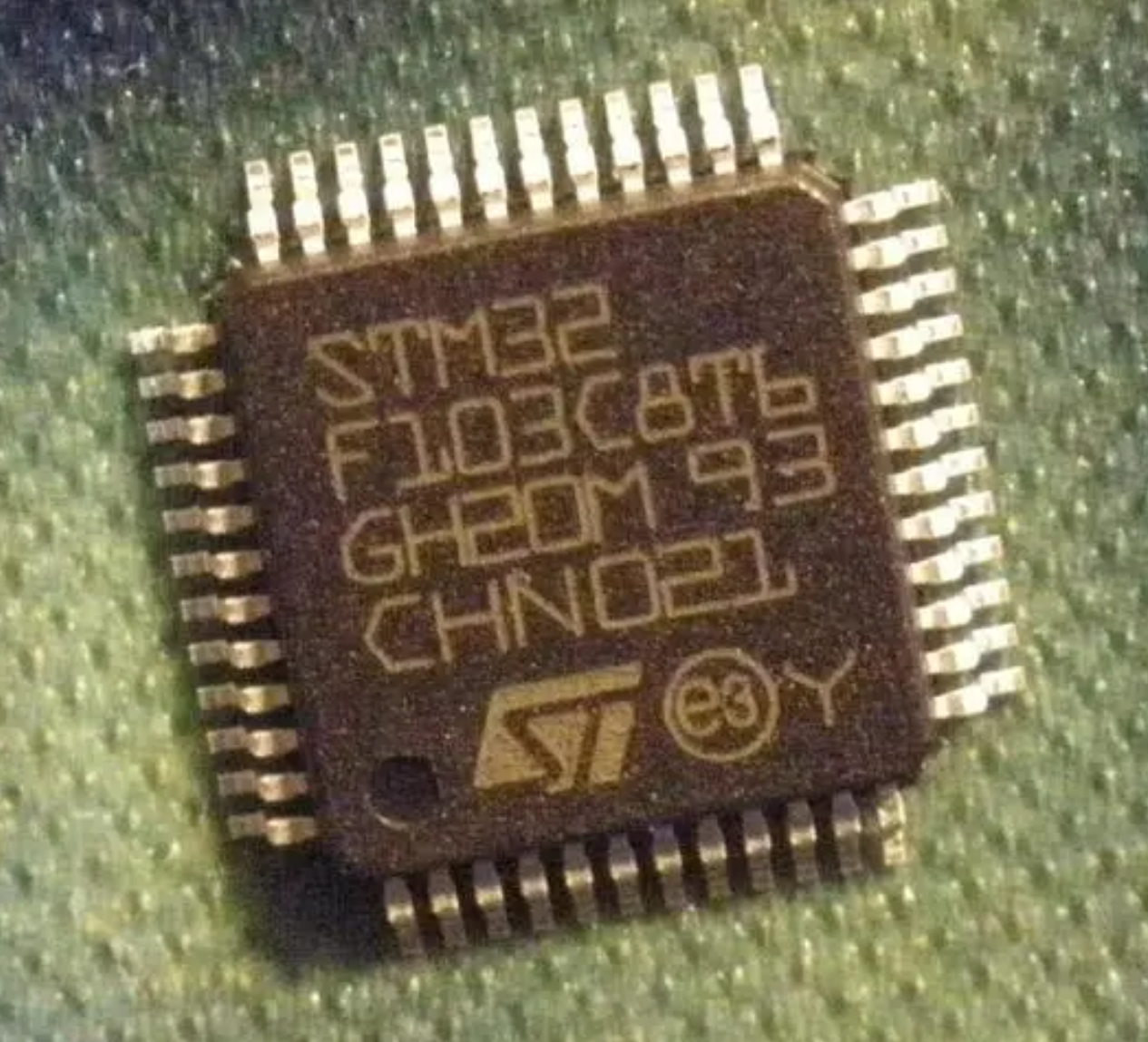
restaurar o microcontrolador STM32F103C8 código do programa flash e copiar o firmware extraído para o novo MCU, a fim de fazer STM32F103C8 clonagem de microprocessador de código binário;
- l all I/O pins are in input mode with a static value at VDD or VSS (no load)
- l all peripherals are disabled unless otherwise mentioned
- l the given value is calculated by measuring the current consumption
- – with all peripherals clocked off
- – with only one peripheral clocked on
- l ambient operating temperature and VDD supply voltage conditions summarized
External clock source characteristics includes below points:
In a given sampling window, either three or six samples of the input signal are taken to determine the validity of the signal. This is determined by the value written to GPxQSELn register to recover stmicro stm32f103c6 mcu flash content.
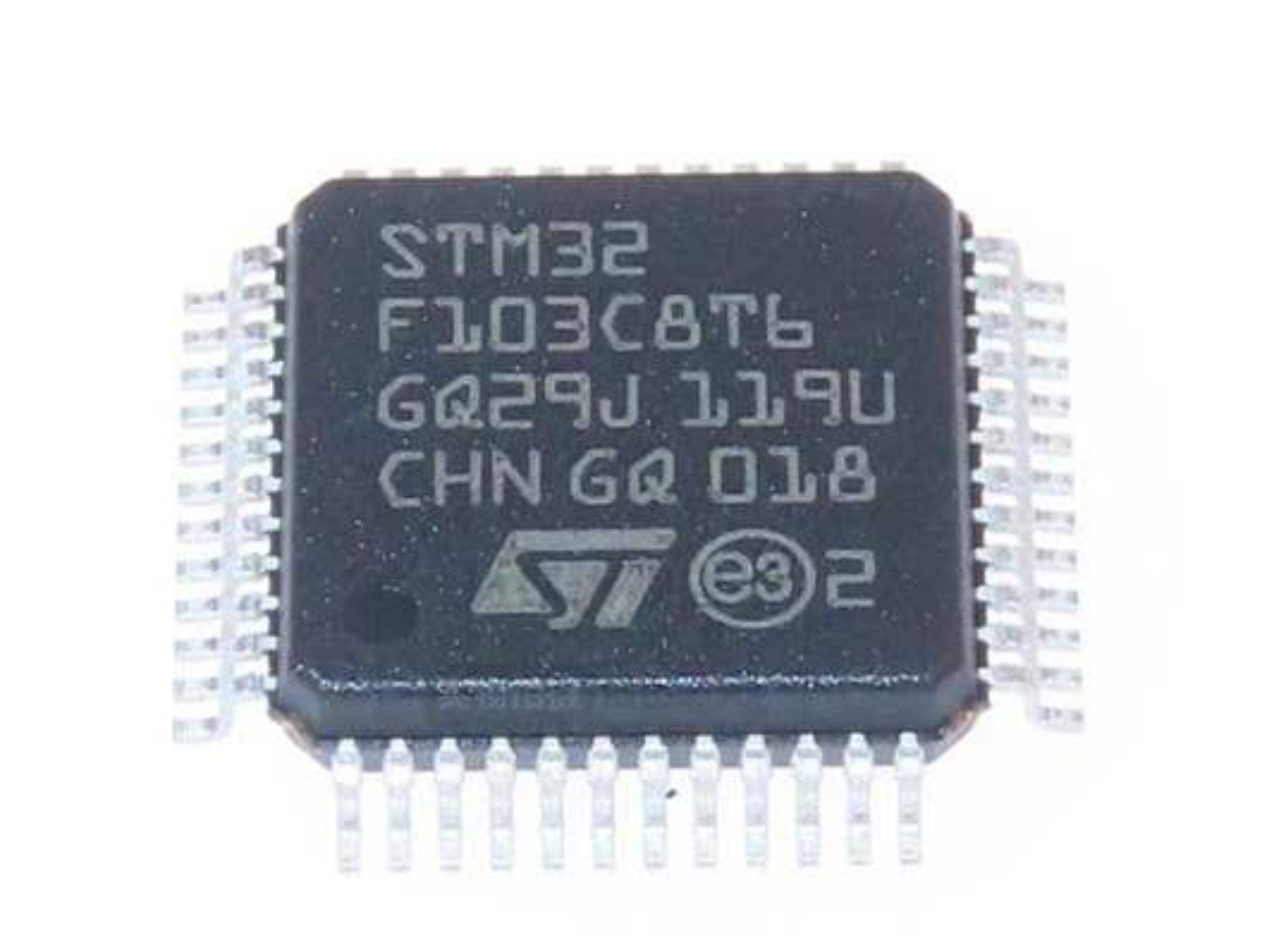
ripristinare il microcontrollore STM32F103C8 il codice del programma flash e copiare il firmware estratto sul nuovo MCU per effettuare STM32F103C8 clonazione del microprocessore in codice binario;
Case 1:
Qualification using three samples
Sampling window width = (SYSCLKOUT cycle × 2 × QUALPRD) × 2, if QUALPRD ≠ 0 Sampling window width = (SYSCLKOUT cycle) × 2, if QUALPRD = 0
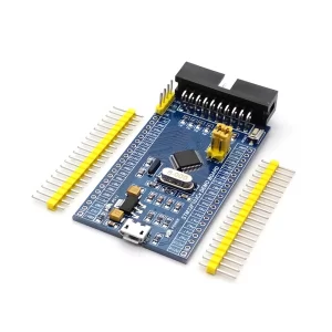
casser données heximales eeprom du microcontrôleur stm32f103c8,
Case 2:
Qualification using six samples Sampling window width = (SYSCLKOUT cycle × 2 × QUALPRD) × 5, if QUALPRD ≠ 0 Sampling window width = (SYSCLKOUT cycle) × 5, if QUALPRD = 0
копировать зашифрованная программа встроенной прошивки MCU stm32f103c8 IC,
Recover STMicro STM32F103C6 MCU Flash Full Content
The stmicroelectronics stm32f103c6 is a widely adopted mcu based on the arm cortex architecture, providing excellent processing capability, low power consumption, and flexible peripheral integration for modern embedded applications. This microcontroller has become a popular choice in industrial automation, consumer electronics, medical equipment, communication devices, automotive control modules, smart instruments, and intelligent monitoring systems.
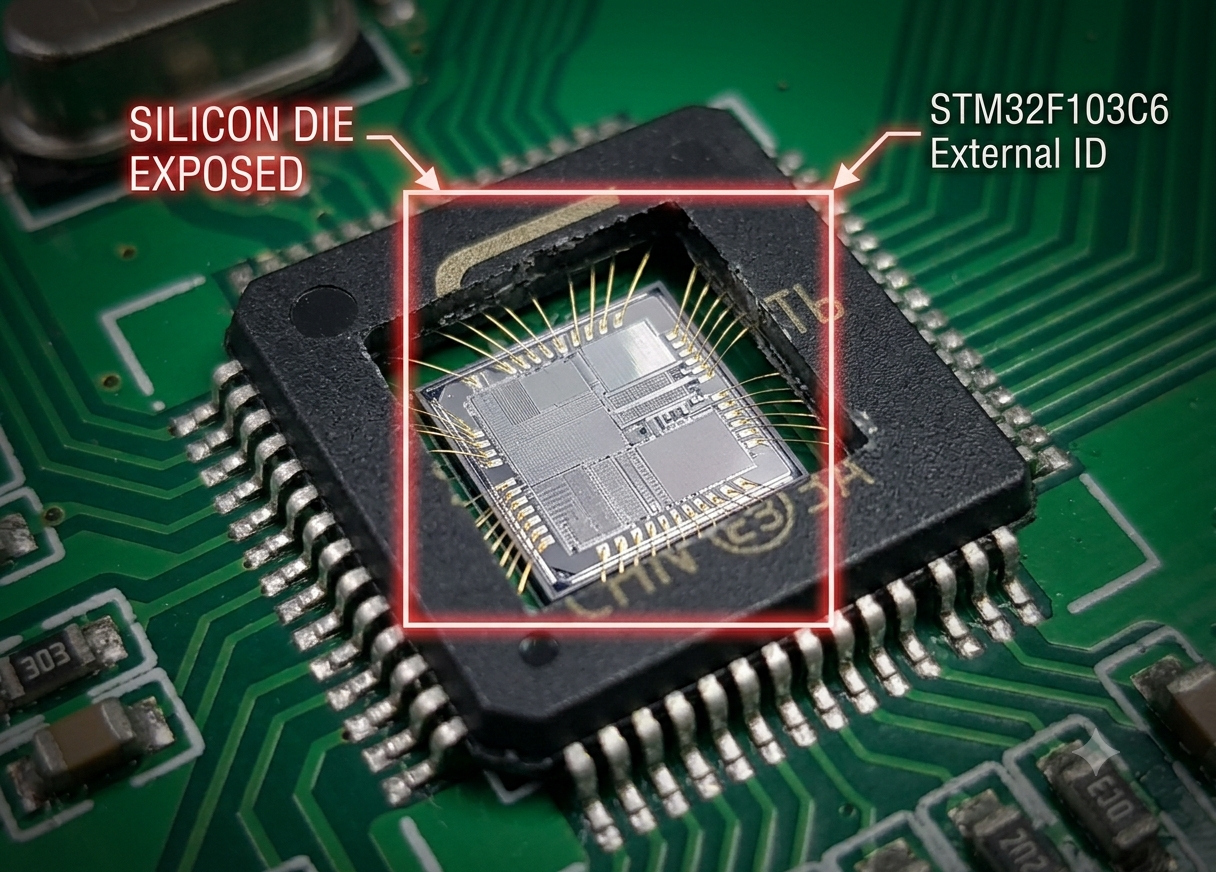
Its compact design and integrated flash memory allow developers to store important firmware, application program instructions, calibration parameters, and operational data directly inside the device. In many commercial products, the internal resources of the chip are configured with protective, protected, locked, secured, or encrypted mechanisms to safeguard valuable software assets. However, as electronic systems remain in service for many years, manufacturers and engineering teams often face challenges caused by missing development documents, unavailable software projects, or lost binary, heximal, source code, and engineering archive files. Recovering full firmware information from legacy hardware becomes essential for maintenance, redesign, compatibility analysis, and long-term product support.
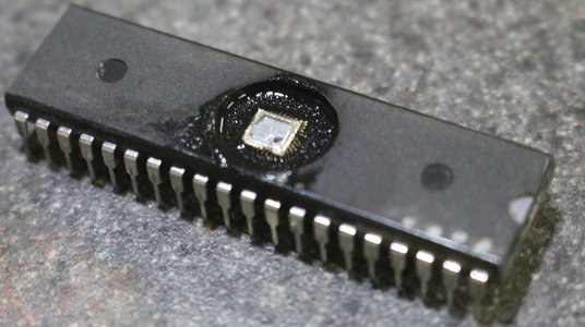
Our “recover stmicro stm32f103c6 mcu flash full content” service focuses on authorized recovery, preservation, and analysis of embedded software resources stored inside the stm32f103c6 mcu. Through advanced engineering evaluation and specialized laboratory workflows, our specialists analyze the internal architecture of the microcontroller, identify available flash regions, and support the recovery of valuable firmware, binary, and configuration data.
Depending on the condition of the target device and project requirements, controlled semiconductor inspection and carefully managed decapsulate analysis may be applied to improve understanding of internal storage structures. Advanced decode methods are used to interpret recovered heximal information, organize fragmented file structures, and rebuild meaningful archive resources. For devices containing locked, protected, or encrypted configurations, our engineers evaluate the architecture and select appropriate recovery approaches based on customer authorization.
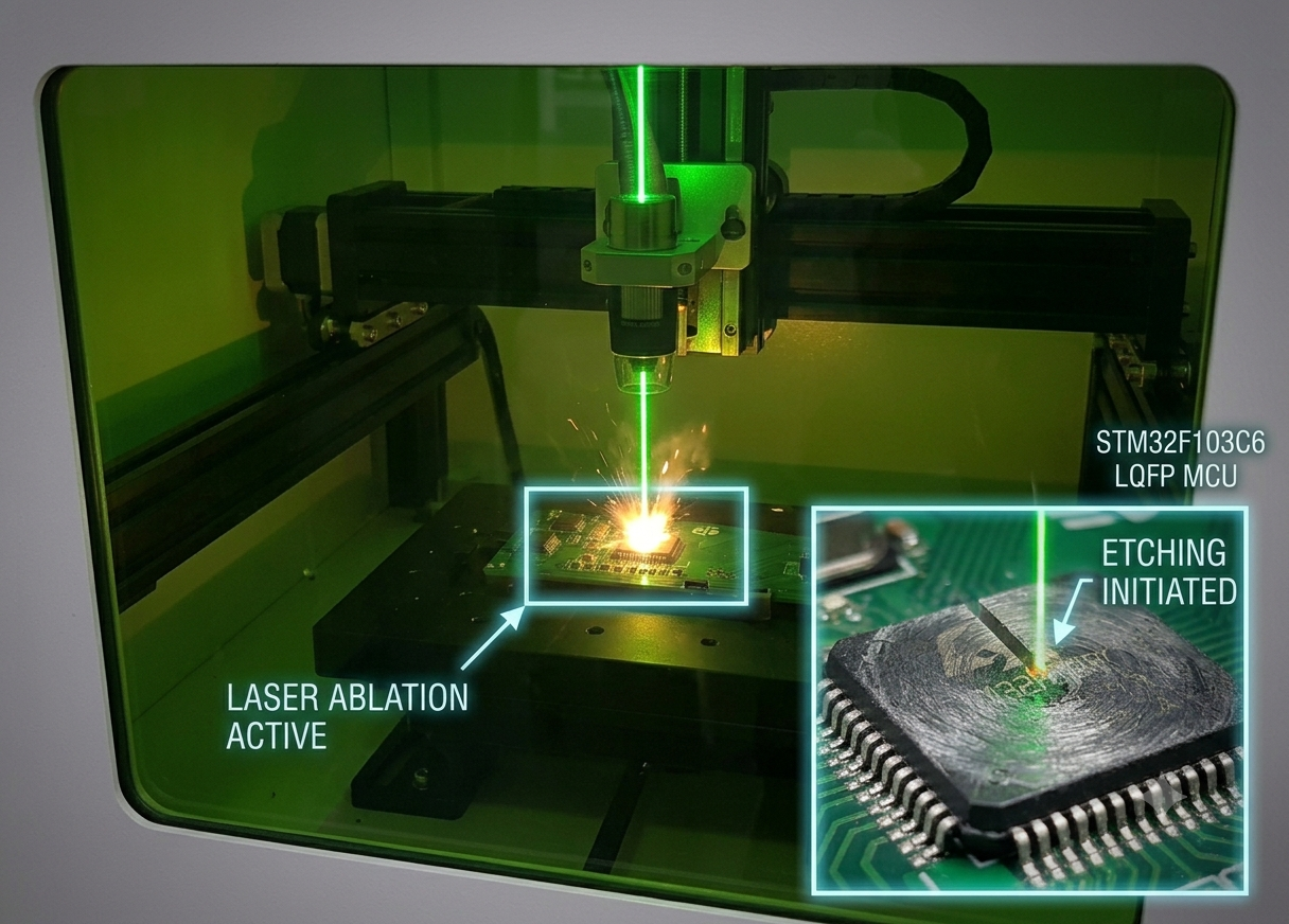
Instead of simply attempting to attack, break, or hack a device, our goal is to preserve valuable engineering information and help customers maintain ownership of their embedded technology. Recovered flash full content, program data, and firmware resources can support product documentation, troubleshooting, system migration, controlled clone development, and duplicate validation for existing designs.
The MCU is placed under the following conditions:
- l All I/O pins are in input mode with a static value at VDD or VSS (no load)
- l All peripherals are disabled except if it is explicitly mentioned
- l Prefetch in on (reminder: this bit must be set before clock setting and bus prescaling)
- l When the peripherals are enabled fPCLK1 = fHCLK, fPCLK2 = fHCLK
The parameters given in below Table are derived from tests performed under the ambient temperature and VDD supply voltage conditions summarized.
- All I/O pins are in input mode with a static value at VDD or VSS (no load)
- All peripherals are disabled except if it is explicitly mentioned
- When the peripherals are enabled fPCLK1 = fHCLK, fPCLK2 = fHCLK, fADCCLK = fPCLK2/2
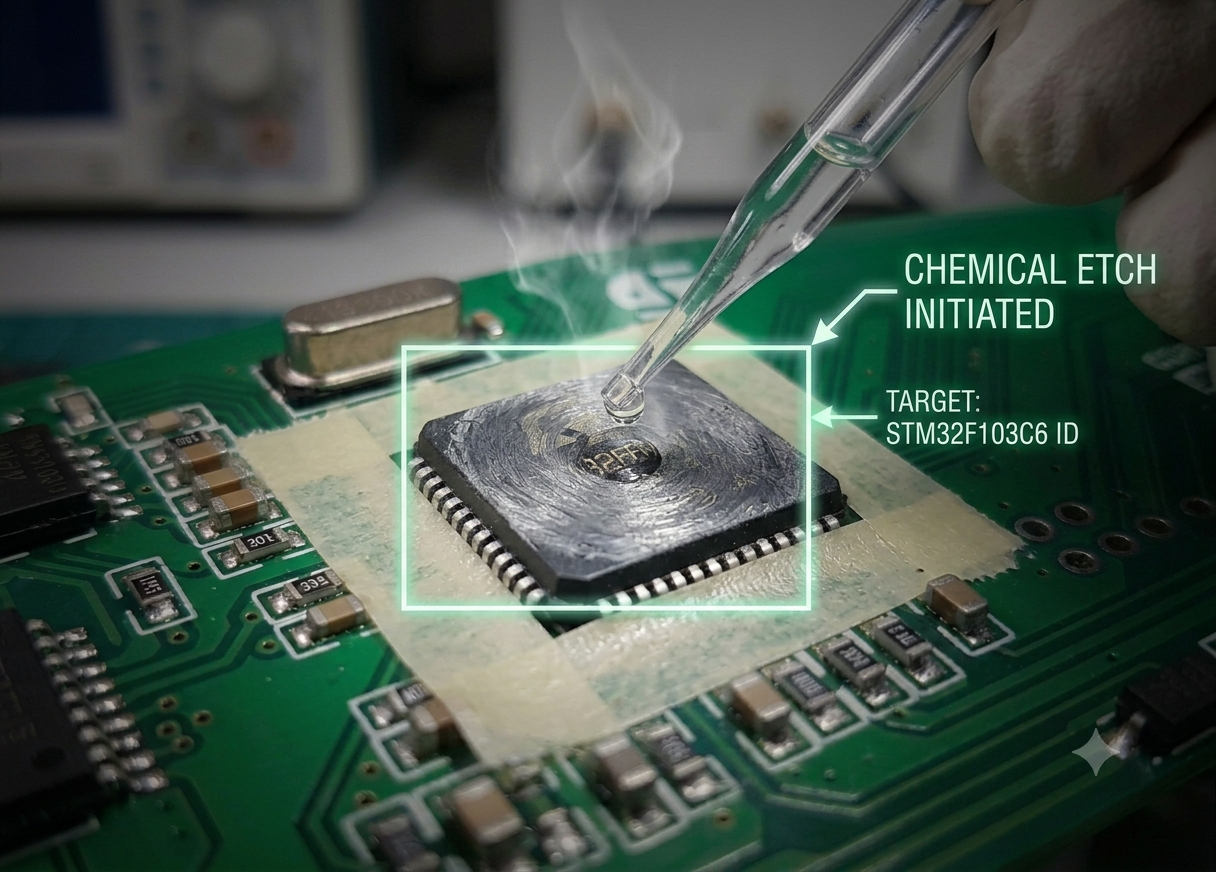
The technical process combines hardware analysis with embedded software reconstruction. Engineers first evaluate the physical condition of the ic, inspect the relationship between the memory structure and firmware operation, and identify the organization of available storage areas. Recovered binary images are carefully analyzed to verify integrity and reconstruct meaningful program sections. Through advanced software tools, engineers can retrieve valuable data, compare firmware behavior, and establish connections between hardware functions and stored application logic.
Where appropriate and authorized, selective decapsulate techniques may provide additional insight into difficult-to-access internal structures of the microprocessor. This methodology helps recover important engineering resources from discontinued or unsupported products where original software environments and development files are no longer available. Although the stm32f103c6 is not a dsp or texas instrument device, its embedded architecture requires the same level of professional analysis applied to complex processor platforms. The recovered source code references, firmware records, and technical archive materials provide practical value for redesign, modernization, maintenance, and lifecycle extension.
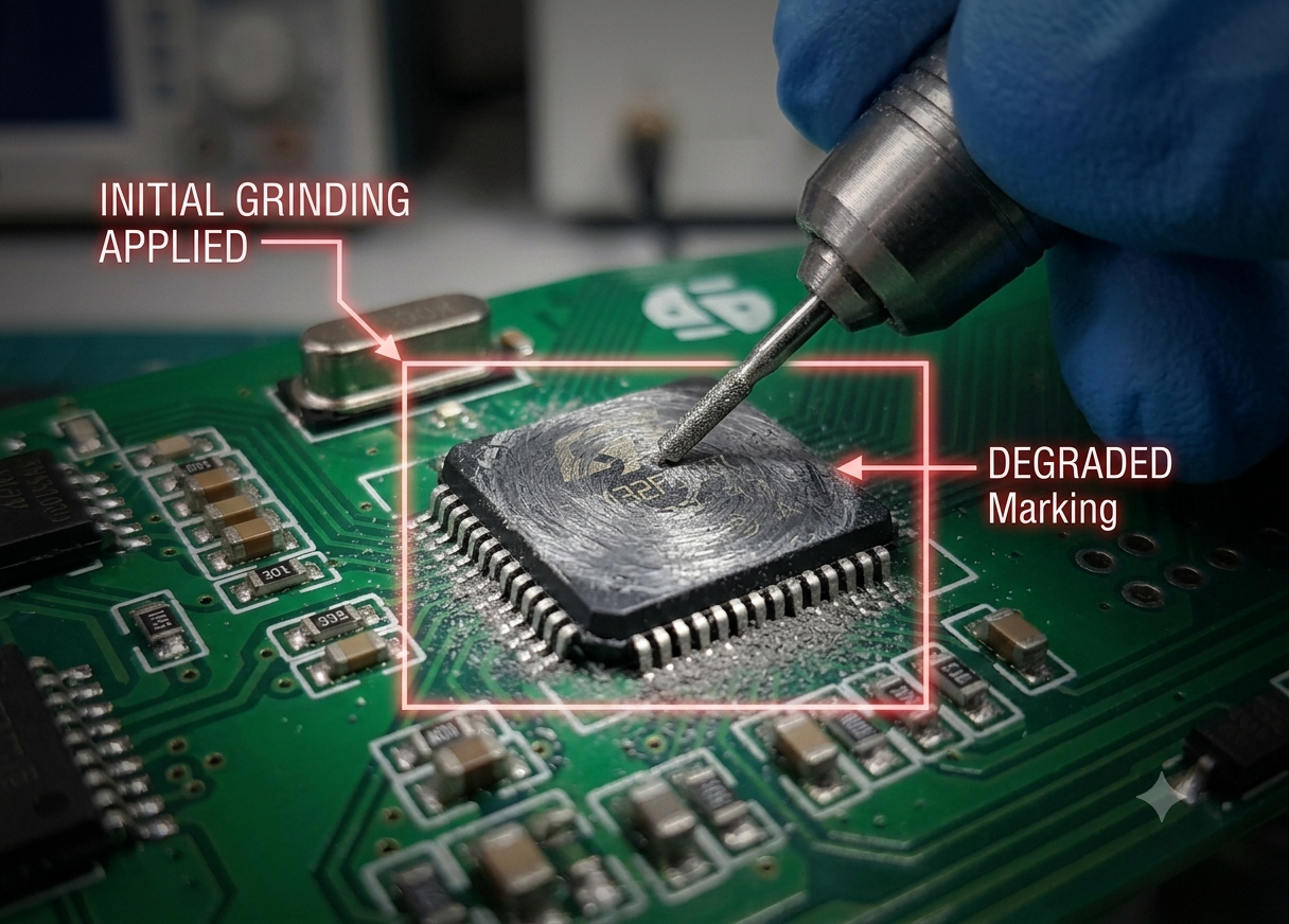
For manufacturers, repair organizations, and engineering teams, recovering stm32f103c6 flash content provides significant benefits for protecting existing investments. Access to historical firmware, validated binary files, reconstructed heximal resources, and organized data archives reduces redevelopment effort and improves product continuity.
Companies can maintain installed equipment, support older product generations, migrate designs to updated platforms, and preserve years of embedded development work. By combining expertise in stmicroelectronics, mcu, microcontroller, and firmware analysis, our service provides a reliable solution for transforming inaccessible chip information into practical engineering resources. Whether the objective is system recovery, technical documentation, product improvement, or long-term maintenance, our capability helps customers preserve critical embedded knowledge and extend the operational life of important electronic systems.
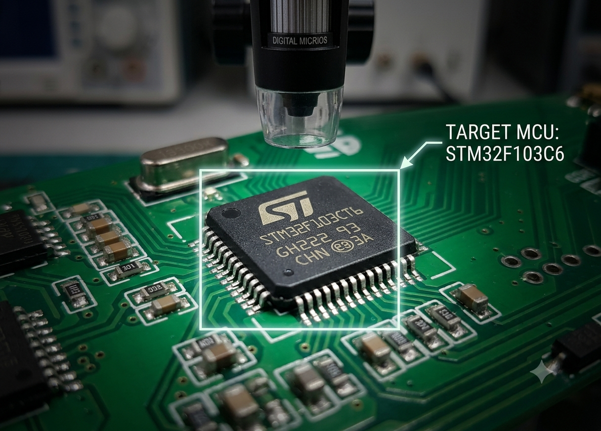
Recovering ARM Microprocessor STM32F103CB Flash Program
Recovering ARM Microprocessor STM32F103CB Flash Program after crack mcu stm32f103cb security fuse bit and disable the protection over the memory content, copy extracted firmware to new MCU;
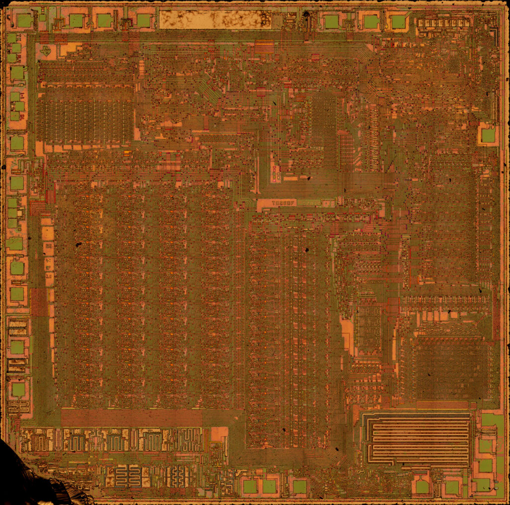
The low-speed external (LSE) clock can be supplied with a 32.768 kHz crystal/ceramic resonator oscillator by Crack STM32F103CB Microcontroller Flash Memory. All the information given in this paragraph are based on characterization results obtained with typical external components specified in below Table.
копировать двоичный файл памяти защищенного микрокомпьютера stm32f103c4
In the application, the resonator and the load capacitors have to be placed as close as possible to the oscillator pins in order to minimize output distortion and startup stabilization time. Refer to the crystal resonator manufacturer for more details on the resonator characteristics when break arm mcu stm32f101cb flash memory (frequency, package, accuracy).
brechen Quellcode der stm32f103c4 MCU-Chip-Speichersoftware,
For CL1 and CL2 it is recommended to use high-quality ceramic capacitors in the 5 pF to 15 pF range selected to match the requirements of the crystal or resonator when Break IC Flash. CL1 and CL2, are usually the same size. The crystal manufacturer typically specifies a load capacitance which is the series combination of CL1 and CL2.
 Posted in Recover MCU |
  Tags: copiar archivo binario de memoria flash del microcontrolador stm32f103c4, copiar Código fuente del software de memoria del chip MCU stm32f103c4, copiar datos de firmware integrados de microordenador stm32f103c4, copiar microprocesador stm32f103c4 flash y programa heximal eeprom |
  Comments Closed
Restoring ARM Microcontroller STM32F103C4 Flash Binary
Restoring ARM Microcontroller STM32F103C4 Flash Binary after crack locked mcu stm32f103c4 security fuse bit and copy extracted firmware to new Microcontroller;
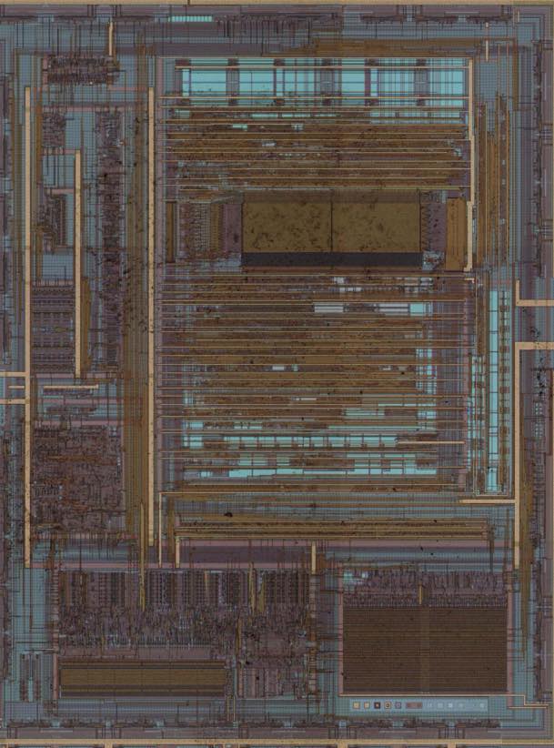
The temperature sensor has to generate a voltage that varies linearly with temperature to Recover MCU content. The conversion range is between 2 V < VDDA < 3.6 V. The temperature sensor is internally connected to the ADC1_IN16 input channel which is used to convert the sensor output voltage into a digital value.
The ARM SWJ-DP Interface is embedded, and is a combined JTAG and serial wire debug port that enables either a serial wire debug or a JTAG probe to be connected to the target of STMicro STM32F101RB MCU flash memory breaking. The JTAG TMS and TCK pins are shared respectively with SWDIO and SWCLK and a specific sequence on the TMS pin is used to switch between JTAG-DP and SW-DP.
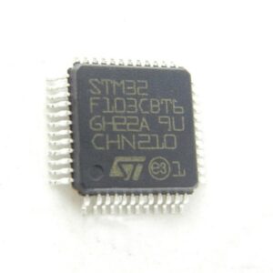
copiar Código fuente del software de memoria del chip MCU stm32f103cB
Unless otherwise specified the minimum and maximum values in the process of Unlock ARM Base STM32F101CB Microprocessor are guaranteed in the worst conditions of ambient temperature, supply voltage and frequencies by tests in production on 100% of the devices with an ambient temperature at TA = 25 °C and TA = TAmax (given by the selected temperature range).
Data based on characterization results, design simulation and/or technology characteristics are indicated in the table footnotes and are not tested in production. Based on characterization, the minimum and maximum values refer to sample tests and represent the mean value plus or minus three times the standard deviation (mean±3S).
копировать двоичный файл памяти защищенного микрокомпьютера stm32f103cb
Unless otherwise specified, typical data are based on TA = 25 °C, VDD = 3.3 V (for the 2 V £ VDD £ 3.6 V voltage range). They are given only as design guidelines and are not tested.
Posted in Recover MCU |
Tags: recobrar archivo binario de memoria flash del microcontrolador stm32f103c4, recobrar Código fuente del software de memoria del chip MCU stm32f103c4, recobrar datos de firmware integrados de microordenador stm32f103c4, recobrar microprocesador stm32f103c4 flash y programa heximal eeprom |
Comments Closed
Duplicate ARM MCU STM32F101CB Memory Content
Duplicate ARM MCU STM32F101CB Memory Content include the program of locked flash memory and data of locked eeprom memory, the tamper resistance system of microcontroller stm32f101cb will be unlocked and embedded binary will extracted from MCU;
The advanced-control timer (TIM1) can be seen as a three-phase PWM multiplexed on 6 channels which can provide great benefit to Unlock ARM Base STM32F101CB Microprocessor. It has complementary PWM outputs with programmable inserted dead times to Copy microcontroller. It can also be seen as a complete general-purpose timer. The 4 independent channels can be used for:
il contenuto della memoria STM32F101CB dell’MCU ARM duplicato include il programma della memoria flash bloccata e i dati della memoria eeprom bloccata, il sistema di resistenza alle manomissioni del microcontrollore stm32f101cb verrà sbloccato e il binario incorporato verrà estratto dall’MCU;
- Input capture
- Output compare
- PWM generation (edge or center-aligned modes)
- One-pulse mode output
The counter can be frozen in debug mode. Many features are shared with those of the standard TIM timers which have the same architecture. The advanced control timer can therefore work together with the TIM timers via the Timer Link feature for synchronization or event chaining to facilitate the progress of recovering locked Microcontroller stm32f101c4 embedded firmware.
There are six synchronizable general-purpose timers embedded in the STM32F100xx devices. Each general-purpose timers can be used to generate PWM outputs, or as simple time base. STM32F100xx devices feature three synchronizable 4-channels general-purpose timers.
дубльований вміст пам’яті ARM MCU STM32F101CB включає програму заблокованої флеш-пам’яті та дані заблокованої пам’яті eeprom, систему захисту від несанкціонованого доступу мікроконтролера STM32F101CB буде розблоковано, а вбудований двійковий файл буде витягнуто з MCU;
These timers are based on a 16-bit auto-reload up/downcounter and a 16-bit prescaler. They feature 4 independent channels each for input capture/output compare, PWM or one-pulse mode output. This gives up to 12 input captures/output compares/PWMs on the largest packages.
ARM Microcontroller STM32F101C4 Locked Firmware Recovery
The STM32F101C4 is a compact and efficient ARM microcontroller widely deployed in modern embedded systems where reliability, processing capability, and low power operation are essential. Based on the ARM Cortex architecture, this MCU is commonly integrated into industrial automation equipment, smart instruments, healthcare electronics, consumer devices, access control systems, communication modules, and intelligent monitoring platforms. Its architecture combines processing performance with integrated flash memory, allowing manufacturers to store operational firmware, application program logic, configuration data, and proprietary control algorithms directly inside the device. To protect intellectual property and prevent unauthorized duplication, these resources are frequently configured as protected, locked, secured, or encrypted, making direct access to binary files, heximal archives, and original source code extremely difficult after production.
The STM32F101C4 value line embeds a nested vectored interrupt controller able to handle up to 41 maskable interrupt channels by Crack STM32F101C4 Microprocessor Flash Memory (not including the 16 interrupt lines of Cortex™-M3) and 16 priority levels.
Closely coupled NVIC gives low latency interrupt processing
Interrupt entry vector table address passed directly to the core
Closely coupled NVIC core interface
Allows early processing of interrupts
Processing of late arriving higher priority interrupts
Support for tail-chaining
Processor state automatically saved
Interrupt entry restored on interrupt exit with no instruction overhead
This hardware block provides flexible interrupt management features with minimal interrupt latency.
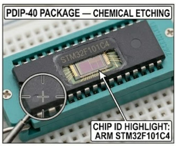
Güvenlik mekanizmalarının bulunduğu durumlarda, ek analiz yöntemleri kullanılarak kilitli, korumalı ve şifrelenmiş ARM STM32F101C4 MCU ortamları üzerinde çalışma gerçekleştirilir ve orijinal program mimarisi yeniden oluşturulur.
Mühendislerimiz geri kazanılan ARM STM32F101C4 mikrodenetleyici veri dosyalarının bütünlüğünü doğrular ve ortaya çıkan kaynak kodunun, hexadecimal çıktıların ve ürün yazılımı yapılarının orijinal gömülü uygulamayla tutarlı kalmasını sağlar.
Sonuç yalnızca bir ARM STM32F101C4 mikroişlemcisi bellek çıkarma süreci değil, erişilemeyen ARM STM32F101C4 mikrodenetleyici içeriğini yeniden kullanılabilir mühendislik verilerine dönüştüren kapsamlı bir veri kurtarma iş akışıdır.
The external interrupt/event controller consists of 18 edge detector lines used to generate interrupt/event requests. Each line can be independently configured to select the trigger event (rising edge, falling edge, both) and can be masked independently. A pending register maintains the status of the interrupt requests. The EXTI can detect an external line with a pulse width shorter than the Internal APB2 clock period. Up to 80 GPIOs can be connected to the 16 external interrupt lines.
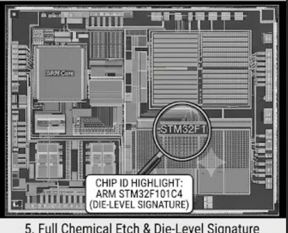
Когато са налични механизми за защита, се използва допълнителен анализ за работа със заключени, защитени и криптирани среди на ARM STM32F101C4 MCU и за възстановяване на оригиналната програмна архитектура.
Нашите инженери проверяват целостта на възстановените файлове с данни от микроконтролера ARM STM32F101C4, като гарантират, че полученият изходен код, шестнадесетичните файлове и структурите на фърмуера остават съвместими с оригиналната вградена реализация.
Резултатът не е просто процес по извличане на паметта на микропроцесора ARM STM32F101C4, а цялостен процес по възстановяване, който преобразува недостъпното съдържание на микроконтролера ARM STM32F101C4 в повторно използваема инженерна информация.
Our “ARM Microcontroller STM32F101C4 Locked Firmware Recovery” service is designed to support customers who require recovery, preservation, or migration of valuable embedded assets stored inside these controllers. By applying advanced semiconductor analysis and specialized recovery workflows, our engineering team can attack, break, and decode complex security implementations to retrieve inaccessible firmware and internal memory data. Depending on the target configuration, controlled decapsulate procedures and electrical analysis may be used to access embedded structures and recover complete binary, heximal, and configuration files from internal flash and associated EEPROM regions. Through careful reconstruction of the extracted archive, we convert raw data into organized program files and interpretable source code structures. This process enables customers to clone, duplicate, maintain, or transition legacy products while preserving functional behavior and system compatibility.
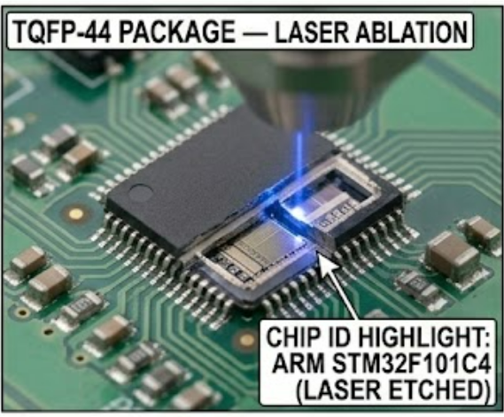
W przypadku obecności mechanizmów zabezpieczeń stosowana jest dodatkowa analiza umożliwiająca pracę z zablokowanymi, chronionymi i szyfrowanymi środowiskami MCU ARM STM32F101C4 oraz rekonstrukcję oryginalnej architektury programu.
Nasi inżynierowie weryfikują integralność odzyskanych plików danych mikrokontrolera ARM STM32F101C4, zapewniając zgodność uzyskanego kodu źródłowego, wyników szesnastkowych oraz struktur firmware z pierwotną implementacją systemu wbudowanego.
Rezultatem nie jest jedynie proces ekstrakcji pamięci mikroprocesora ARM STM32F101C4, lecz kompletny proces odzyskiwania, który przekształca niedostępną zawartość mikrokontrolera ARM STM32F101C4 w informacje inżynieryjne gotowe do ponownego wykorzystania.
The technical approach combines physical access methods with advanced software interpretation technologies. Silicon-level inspection and selective decapsulation allow low-level retrieval of protected memory regions, while proprietary tools process extracted binary data and perform deep decode operations to rebuild coherent firmware archives. When security mechanisms are present, additional analysis is used to work through locked, protective, and encrypted environments and reconstruct the original program architecture. Our engineers validate the integrity of recovered data files, ensuring that the resulting source code, heximal outputs, and firmware structures maintain consistency with the original embedded implementation. The result is not simply a memory extraction process but a complete recovery workflow that transforms inaccessible device content into reusable engineering information.
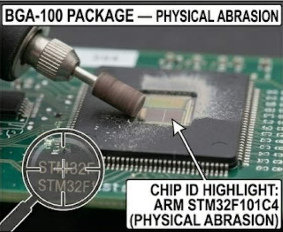
За наявності механізмів безпеки застосовується додатковий аналіз для роботи із заблокованими, захищеними та зашифрованими середовищами MCU ARM STM32F101C4 і відновлення оригінальної архітектури програмного забезпечення.
Наші інженери перевіряють цілісність відновлених файлів даних мікроконтролера ARM STM32F101C4, забезпечуючи відповідність отриманого вихідного коду, шістнадцяткових файлів та структур прошивки початковій вбудованій реалізації.
Результатом є не просто процес вилучення пам’яті мікропроцесора ARM STM32F101C4, а повний цикл відновлення, який перетворює недоступний вміст мікроконтролера ARM STM32F101C4 на інженерні дані, придатні для повторного використання.
For end users, recovering STM32F101C4 firmware delivers substantial operational advantages. Organizations facing discontinued hardware, unavailable development resources, or long product lifecycles can regain access to essential embedded data without redesigning an entire platform. Recovered binary archives support maintenance, hardware migration, software validation, and controlled system replication. By preserving original program files and enabling accurate duplication, customers reduce engineering effort, shorten recovery timelines, and extend the usable life of proven electronic products. Our expertise in recovering secured ARM firmware provides a dependable path for restoring valuable technical assets and maintaining continuity across critical embedded applications.
Pokud jsou přítomny bezpečnostní mechanismy, používá se dodatečná analýza pro práci se zamčenými, chráněnými a šifrovanými prostředími MCU ARM STM32F101C4 a rekonstrukci původní programové architektury.
Naši inženýři ověřují integritu obnovených datových souborů mikrokontroléru ARM STM32F101C4 a zajišťují, aby výsledný zdrojový kód, hexadecimální výstupy a struktury firmwaru odpovídaly původní implementaci vestavěného systému.
Výsledkem není pouze proces extrakce paměti mikroprocesoru ARM STM32F101C4, ale kompletní proces obnovy, který převádí nepřístupný obsah mikrokontroléru ARM STM32F101C4 na znovu využitelné technické informace.
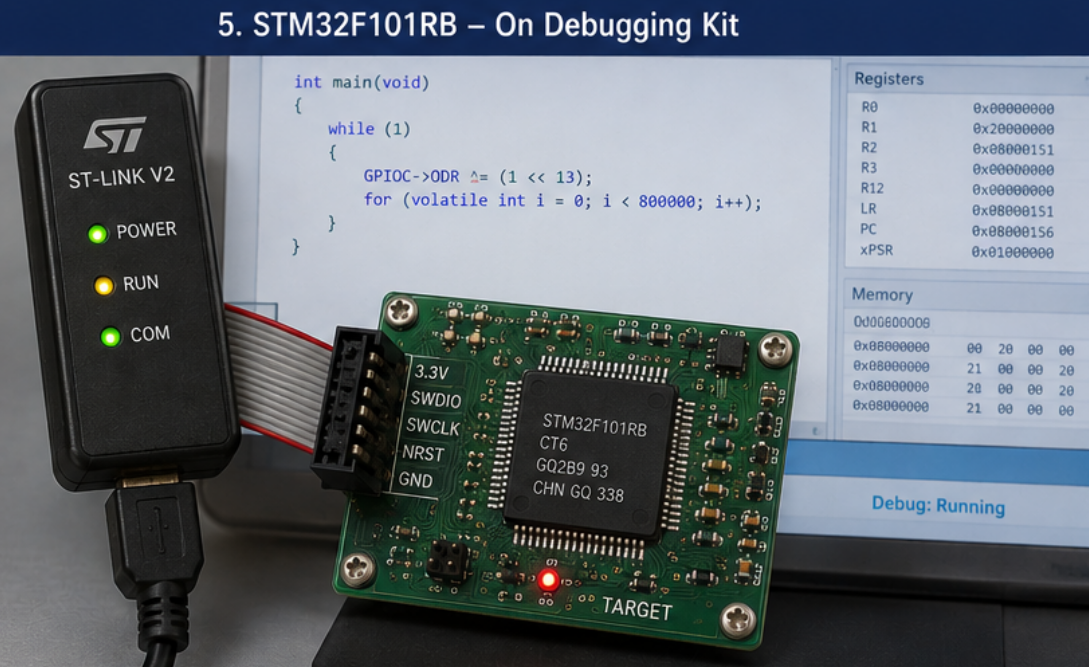
Break ARM Microcontroller STM32F101RB Flash Memory
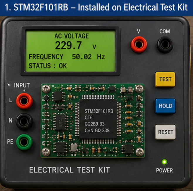
The STM32F101RB microcontroller represents an incredibly robust and versatile piece of silicon architecture, engineered on a 32-bit ARM Cortex-M3 processor core running up to 36 MHz. This highly reliable device is frequently integrated as the central execution engine within mission-critical utility grid systems, clinical medical apparatus, smart barcode scanners, and intricate environmental control sub-assemblies. Featuring distinct peripheral parameters like its 7-channel DMA controller, 12-bit Analog-to-Digital converters, and an array of communication interfaces such as USART, I2C, and SPI, this chip excels at processing real-time telemetry. Its embedded firmware is housed in a high-density, on-chip storage area designed to keep proprietary device logic running autonomously for decades. However, industrial businesses frequently run into immediate production roadblocks when a legacy platform must be serviced or migrated, but the initial documentation, source code files, or master engineering libraries have been completely lost to time. When critical components become obsolete or supplier access vanishes, establishing a trustworthy mechanism to read out the internal configuration becomes a major priority. Our elite laboratory specializes in precision hardware manipulation designed to break ARM Microcontroller STM32F101RB Flash Memory architectures, providing a trusted option to recover your original design assets.
The TIM2, TIM3, TIM4 general-purpose timers can work together or with the TIM1 advanced-control timer via the Timer Link feature for synchronization or STMicro STM32F101RB MCU Cracking.
TIM2, TIM3, TIM4 all have independent DMA request generation.
These timers are capable of handling quadrature (incremental) encoder signals and the digital outputs from 1 to 3 hall-effect sensors. Their counters can be frozen in debug mode. Overcoming the high-grade internal security layout of an enterprise-level microcontroller requires navigating sophisticated hardware-level reading barriers natively deployed to shield proprietary software assets. To carefully attack, break, and decode these complex internal hardware-level locks, our engineering lab implements a rigorous, non-destructive physical and electrical procedure.
Tescilli kontrol kodunuz eski bir çevresel PLD matrisi içinde, harici bellek yongalarında veya doğrudan ARM STM32F101RB mikrodenetleyicisinin çekirdek mikro mimarisinde bulunuyor olsun, özel okuma araçlarımız operasyonel verilerin eksiksiz bir kopyasını güvenli şekilde elde edebilir.
Ekibimiz ham veri akışını başarıyla geri aldıktan sonra, mühendisler tam operasyonel parametreleri modern ve kolay temin edilebilen bir ARM STM32F101RB mikrodenetleyicisine aktarabilir. Bu kapsamlı veri çıkarma süreci, orijinal cihaz davranışının aynı şekilde yeniden oluşturulmasını sağlar.
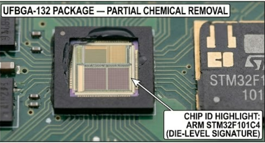
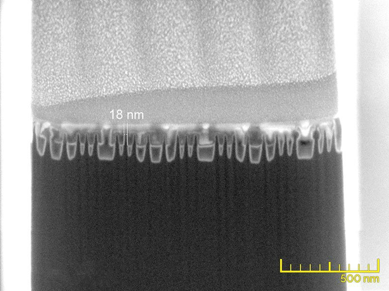
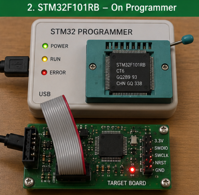
Initially, specialized technicians decapsulate the outer epoxy molding of the integrated circuit with chemical precision, exposing the bare silicon die and its sub-micron layout underneath. Once the internal structures are fully visible under advanced microscopic imaging, we can analyze the status of the embedded protective code fuses. By utilizing deep-precision micro-probing techniques or targeted optical signal modification directly on the physical registers, our team can carefully bypass the internal security bits that restrict reading access via the JTAG or Serial Wire Debug ports. This precise intervention allows us to extract the completely untouched binary data straight from the inner flash and protected eeprom sectors without corrupting the physical substrate. The definitive deliverable from this advanced engineering operation is a completely pristine, uncorrupted heximal file that contains a flawless structural mirror of your system’s original configuration.
The TIM15, TIM16 and TIM17 timers can work together, and TIM15 can also operate with TIM1 via the Timer Link feature for synchronization or event chaining. TIM15 can be synchronized with TIM16 and TIM17.
TIM15, TIM16, and TIM17 have a complementary output with dead-time generation and independent DMA request generation Their counters can be frozen in debug mode. These timers are mainly used for DAC trigger generation. They can also be used as a generic 16-bit time base. The fundamental purpose of choosing to hack, duplicate, or extract code from a heavily secured microcontroller layout is to eliminate single-point supply chain failures and secure a company’s long-term technical autonomy.
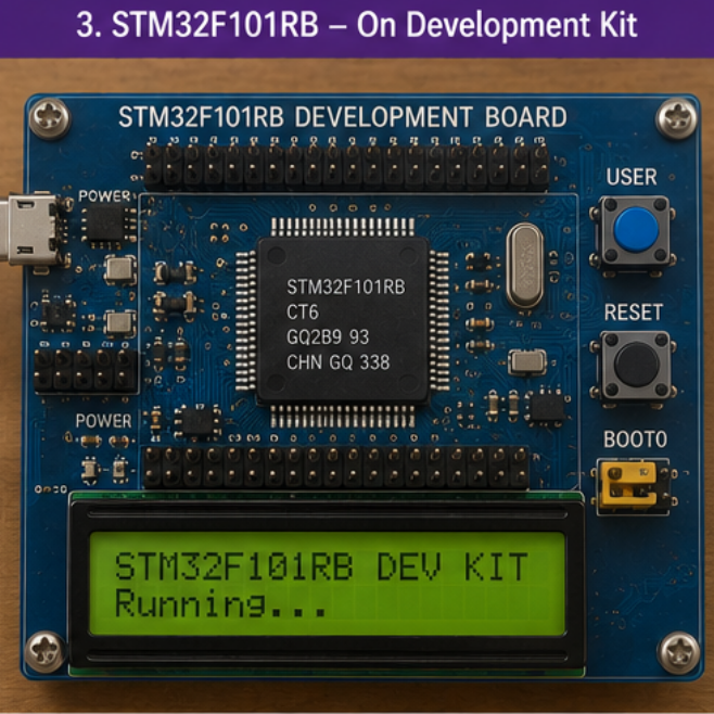
When engineering teams lose access to their original program archive, our advanced laboratory recovery techniques provide an efficient way to recover the vital machinery instructions before a full-scale, incredibly expensive system redesign is forced upon your budget. Whether your proprietary control code is isolated inside an older peripheral PLD matrix, external memory chips, or the core micro-architecture of the ARM chip itself, our custom reading tools can extract the complete operational file safely. After our team successfully retrieves the raw data stream, engineers can easily clone the full operational parameters onto a modern, readily available replacement microcontroller. This comprehensive data extraction allows you to duplicate the original device behavior exactly, giving your manufacturing team a clean, verified engineering archive to resume board production without risking a single day of system downtime.
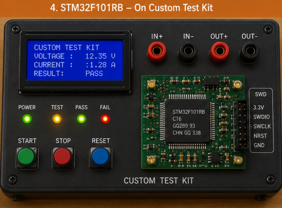
Partnering with an experienced technical team to unlock and recover embedded system software delivers major financial, operational, and strategic benefits to project managers, maintenance engineers, and hardware developers alike. Instead of exhausting immense corporate capital and spending quarters of valuable engineering time trying to reverse-engineer and re-write complex embedded applications from scratch—a risky process that notorious introduces hidden software bugs—our advanced extraction pipeline delivers a fast, precise path to a fully verified binary file. This complete structural continuity ensures that every newly generated duplicate circuit board matches the exact performance and behavioral profile of the field-tested units your clients already trust. By utilizing our specialized microcontroller recovery solutions, your enterprise effectively mitigates the existential threats of part obsolescence, safeguards vital corporate intellectual property, and secures a fully predictable roadmap for your industrial hardware investments for many years to come.