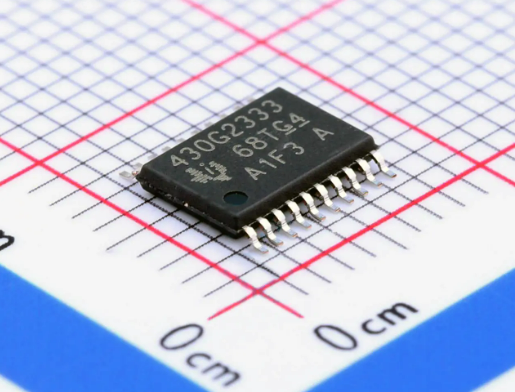
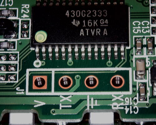
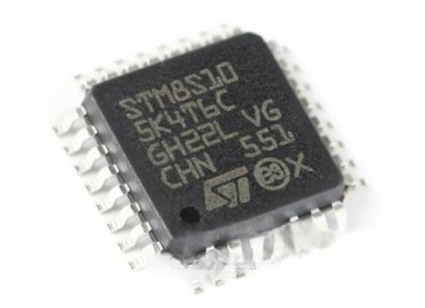
 Texas MSP430G2333 Microcontroller Firmware Recovery
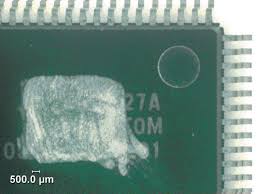
Texas MSP430G2333 Microcontroller Firmware Recovery needs to crack ti msp430g2333 microprocessor’s security tamper resistance system, and then extract microprocessor msp430g2333 locked code from its flash memory;

Stresses beyond those listed under “absolute maximum ratings” may cause permanent damage to the device. These are stress ratings only, and functional operation of the device at these or any other conditions beyond those indicated under “recommended operating conditions” is not implied. Exposure to absolute-maximum-rated conditions for extended periods may affect device reliability.
Texas MSP430G2333 mikrodenetleyici ürün yazılımı kurtarma, ti msp430g2333 mikroişlemcinin güvenlik kurcalama direnci sistemini kırmalı ve ardından mikroişlemci msp430g2333 kilitli kodunu flash belleğinden çıkarmalıdır;
All voltages referenced to VSS. The JTAG fuse-blow voltage, VFB, is allowed to exceed the absolute maximum rating. The voltage is applied to the TEST pin when blowing the JTAG fuse which is a common method for cracking msp430g2230 mcu flash memory fuse bit.
unlock silicon microcontroller MSP430G2333 flash memory and copy heximal program of memory
Higher temperature may be applied during board soldering according to the current JEDEC J-STD-020 specification with peak reflow temperatures not higher than classified on the device label on the shipping boxes or reels.
The MSP430 CPU is clocked directly with MCLK. Both the high and low phase of MCLK must not exceed the pulse duration of the specified maximum frequency when restoring msp430g2001 microcontroller heximal program.
Modules might have a different maximum input clock specification. See the specification of the respective module in this data sheet.
Crack Texas Instrument MSP430G2230 MCU Flash Memory
Crack Texas Instrument MSP430G2230 MCU Flash Memory needs to decapsulate MSP430G2230 by chemical solution and unlock microcontroller tamper resistance system, extract embedded source code from TI IC chip;
Universal Serial Communications Interface (USCI)
The USCI module is used for serial data communication. The USCI module supports synchronous communication protocols such as SPI (3 or 4 pin) and I2C, and asynchronous communication protocols such as UART, enhanced UART with automatic baudrate detection (LIN), and IrDA. Not all packages support the USCI functionality.
çatlak Texas Instrument MSP430G2230 MCU flash belleğin MSP430G2230’u kimyasal çözelti ile kapsülünü çözmesi ve mikrodenetleyici kurcalama direnci sisteminin kilidini açması, gömülü kaynak kodunu TI IC yongasından çıkarması gerekir
USCI_A0 provides support for SPI (3 or 4 pin), UART, enhanced UART, and IrDA. USCI_B0 provides support for SPI (3 or 4 pin) and I2C.
Comparator_A+
The primary function of the comparator_A+ module is to support precision slope analog-to-digital conversions, battery-voltage supervision, and monitoring of external analog signals.
ADC10 (MSP430G2x53 Only)
The ADC10 module supports fast 10-bit analog-to-digital conversions. The module implements a 10-bit SAR core, sample select control, reference generator, and data transfer controller (DTC) for automatic conversion result handling by replicating msp430g2231 cpu flash memory file, allowing ADC samples to be converted and stored without any CPU intervention.
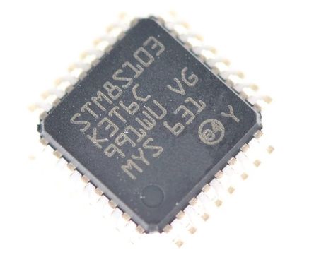
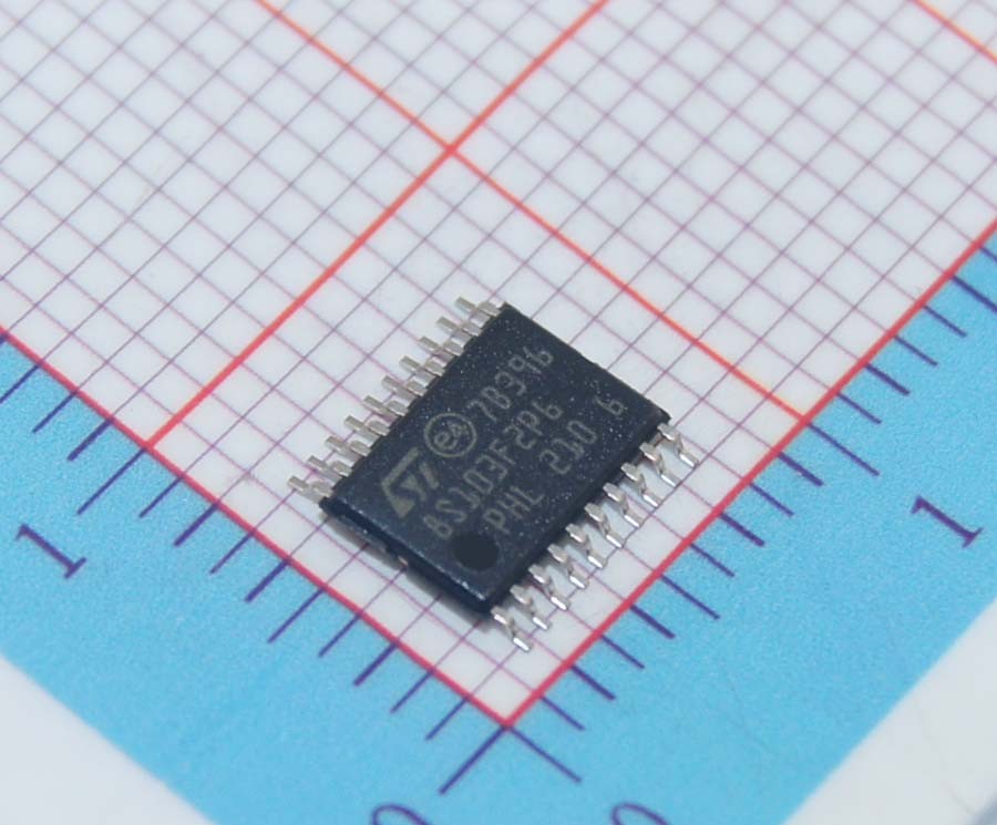
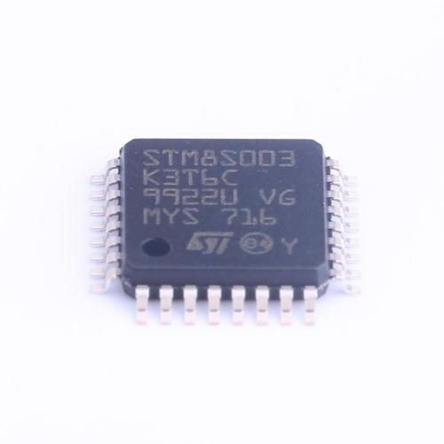
STM8S103K3T6 Microcontroller Embedded Flash Firmware Restoration
STM8S103K3T6 Microcontroller Embedded Flash Firmware Restoration starts from unlock stm8s103k3 security fuse bit by focus ion beam and then extract flash memory code from original stm8s103k3 processor;

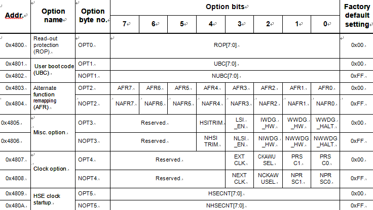
Option bytes contain configurations for device hardware features as well as the memory protection of the device. They are stored in a dedicated block of the memory. Except for the ROP (read-out protection) byte, each option byte has to be stored twice, in a regular form (OPTx) and a complemented one (NOPTx) for redundancy when recover stm8s003k3 memory heximal.
STM8S103K3T6 mikrodenetleyici gömülü flash ürün yazılımı geri yükleme, STM8S103K3 güvenlik sigortasının odak iyon ışını ile bit kilidini açmaktan başlar ve ardından orijinal STM8S103K3 işlemciden flash bellek kodunu çıkarır;
Option bytes can be modified in ICP mode (via SWIM) by accessing the EEPROM address shown in Table 12: Option bytes below. Option bytes can also be modified ‘on the fly’ by the application in IAP mode, except the ROP option that can only be modified in ICP mode (via SWIM).
Refer to the STM8S Flash programming manual (PM0051) and STM8 SWIM communication protocol and debug module user manual (UM0470) for information on SWIM programming procedures in the process of stm8s103k2 mcu flash source code cloning.
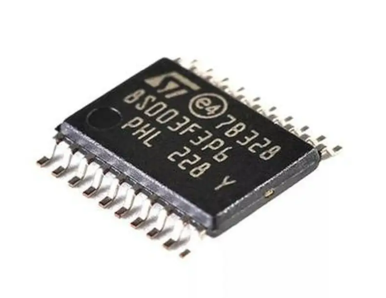
STMicro STM8S103F3P6 MCU Chip Breaking
STMicro STM8S103F3P6 MCU Chip Breaking refers to flash memory of CPU STM8S103F3P6 tamper resistance system unlocking and then readout embedded heximal from microcontroller stm8s103f3 flash memory;
SPI
Maximum speed: 8 Mbit/s (fMASTER/2) both for master and slave
Full duplex synchronous transfers
Simplex synchronous transfers on two lines with a possible bidirectional data line
Master or slave operation – selectable by hardware or software
CRC calculation
1 byte Tx and Rx buffer
Slave/master selection input pin
I2C
I2C master featuresClock generationStart and stop generationI2C slave featuresProgrammable I2C address detectionStop bit detectionGeneration and detection of 7-bit/10-bit addressing and general callSupports different communication speedsStandard speed (up to 100 kHz)Fast speed when breaking micro stm8s103f3 flash memory (up to 400 kHz).
As shown in the rightmost column of the pin description table, some alternate functions can be remapped at different I/O ports by programming one of eight AFR (alternate function remap) option bits.
Refer to Section 8: Option bytes. When the remapping option is active, the default alternate function is no longer available in the process of breaking stm8s103k3 microcontroller protection.
To use an alternate function, the corresponding peripheral must be enabled in the peripheral registers. Alternate function remapping does not effect GPIO capabilities of the I/O ports (see the GPIO section of the family reference manual, RM0016).
Break STM8S103F3P3 Micro CPU Flash Memory
Break STM8S103F3P3 Micro CPU Flash Memory will help engineer make stm8s103f3p3 mcu flash code cloning, the original heximal will be extracted from embedded flash and eeprom memory;
The window watchdog is used to detect the occurrence of a software fault, usually generated by external interferences or by unexpected logical conditions, which cause the application program to abandon its normal sequence.
The window function can be used to trim the watchdog behavior to match the application perfectly after stm8s003k3 microcontroller flash memory recovery.
romper la memoria flash de la CPU del microcontrolador STM8S103F3P3 ayudará al ingeniero a hacer clonación de código flash MCU stm8s103f3p3, el heximal original se extraerá de la memoria flash y eeprom integrada;
The application software must refresh the counter before time-out and during a limited time window.
A reset is generated in two situations:
Timeout: at 16 MHz CPU clock the time-out period can be adjusted between 75 µs up to 64 ms.
Refresh out of window: the down-counter is refreshed before its value is lower than the one stored in the window register.
The independent watchdog peripheral can be used to resolve processor malfunctions due to hardware or software failures which can be used for copying stm8s003f3 microprocessor flash content.
It is clocked by the 128 kHz LSI internal RC clock source, and thus stays active even in case of a CPU clock failure
The IWDG time base spans from 60 µs to 1 s.
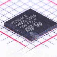
Break STM8S103K3U6 MCU Protection
Break STM8S103K3U6 MCU Protection can disable the security fuse bit of microcontroller stm8s103k3 through hacking technique and then readout the embedded firmware from stm8s103k3u6 flash and eeprom memory;
For efficient power management, the application can be put in one of four different low- power modes. You can configure each mode to obtain the best compromise between the lowest power consumption, the fastest start-up time and available wakeup sources.
Wait mode: In this mode, the CPU is stopped, but peripherals are kept running. The wakeup is performed by an internal or external interrupt or reset.
romper la protección del MCU STM8S103K3U6 puede desactivar el bit de fusible de seguridad del microcontrolador stm8s103k3 a través de la técnica de piratería y luego leer el firmware integrado de la memoria flash y eeprom stm8s103k3u6;
Active halt mode with regulator on: In this mode, the CPU and peripheral clocks are stopped. An internal wakeup is generated at programmable intervals by the auto wake up unit (AWU) to clone stm8s103f2 memory source code.
The main voltage regulator is kept powered on, so current consumption is higher than in active halt mode with regulator off, but the wakeup time is faster. Wakeup is triggered by the internal AWU interrupt, external interrupt or reset.
Active halt mode with regulator off: This mode is the same as active halt with regulator on, except that the main voltage regulator is powered off, so the wake up time is slower when copying microprocessor stm8s003f3 flash memory content.
Halt mode: In this mode the microcontroller uses the least power. The CPU and peripheral clocks are stopped, the main voltage regulator is powered off. Wakeup is triggered by external event or reset.
STMicroelectronic STM8S105K4 MCU Protective Memory Breaking
STMicroelectronic STM8S105K4 MCU Protective Memory Breaking will remove the fuse bit of microcontroller by cracking technique and readout embedded firmware from microprocessor flash memory;

Interrupt controller
- Nested interrupts with three software priority levels
- 32 interrupt vectors with hardware priority
- Up to 27 external interrupts on six vectors including TLI
- Trap and reset interrupts
Flash program memory and data EEPROM
- 8 Kbyte of Flash program single voltage Flash memory
- 128 byte true data EEPROM
- User option byte area
Write protection (WP)
Write protection of Flash program memory and data EEPROM is provided to avoid unintentional overwriting of memory that could result from a user software malfunction after cloning mcu stm8s103f2 source code.
STMicroelectronic STM8S105K4 MCU La rotura de la memoria protectora eliminará el bit de fusible del microcontrolador mediante la técnica de craqueo y la lectura del firmware integrado de la memoria flash del microprocesador;
There are two levels of write protection. The first level is known as MASS (memory access security system). MASS is always enabled and protects the main Flash program memory, data EEPROM and option bytes.
To perform in-application programming (IAP), this write protection can be removed by writing a MASS key sequence in a control register. This allows the application to modify the content of main program memory and data EEPROM when copying microprocessor stm8s003f3 flash memory content, or to reprogram the device option bytes. A second level of write protection, can be enabled to further protect a specific area of memory known as UBC (user boot code).
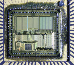
Clone MCU STM8S103F2 Flash Source Code
Clone MCU STM8S103F2 Flash Source Code from original Microcontroller STM8S103F2 by unlocking processor stm8s103f2 tamper resistance system and then extract embedded firmware from flash and eeprom memory;
The 8-bit STM8 core is designed for code efficiency and performance.
It contains six internal registers which are directly addressable in each execution context, 20 addressing modes including indexed indirect and relative addressing and 80 instructions.
Architecture and registers

clonar o código-fonte flash MCU STM8S103F2 do microcontrolador STM8S103F2 original desbloqueando o sistema de resistência à violação do processador STM8s103f2 e, em seguida, extrair o firmware incorporado da memória flash e eeprom;
- Harvard architecture
- 3-stage pipeline
- 32-bit wide program memory bus – single cycle fetching for most instructions
- X and Y 16-bit index registers – enabling indexed addressing modes with or without offset and read-modify-write type data manipulations
- 8-bit accumulator
- 24-bit program counter – 16-Mbyte linear memory space
- 16-bit stack pointer – access to a 64 K-level stack
- 8-bit condition code register – 7 condition flags for the result of the last instruction
Addressing
- 20 addressing modes
- Indexed indirect addressing mode for look-up tables located anywhere in the address space
- Stack pointer relative addressing mode for local variables and parameter passing
Instruction set
- 80 instructions with 2-byte average instruction size
- Standard data movement and logic/arithmetic functions
- 8-bit by 8-bit multiplication
- 16-bit by 8-bit and 16-bit by 16-bit division
- Bit manipulation
- Data transfer between stack and accumulator (push/pop) with direct stack access
- Data transfer using the X and Y registers or direct memory-to-memory transfers
Copy STM8S003F3 Microprocessor Flash Memory Content
Copy STM8S003F3 Microprocessor Flash Memory Content needs to unlock stmicroelectronics mcu stm8s003f3 security fuse bit and then readout microcontroller flash memory file;
The following section intends to give an overview of the basic features of the STM8S003F3/K3 value line functional modules and peripherals. For more detailed information please refer to the corresponding family reference manual (RM0016).
copiar STM8S003F3 microprocessador conteúdo de memória flash precisa desbloquear stmicroelectronics mcu stm8s003f3 fusível bit e, em seguida, ler arquivo de memória flash microcontrolador;
The 8-bit STM8 core is designed for code efficiency and performance. It contains six internal registers which are directly addressable in each execution context, 20 addressing modes including indexed indirect and relative addressing and 80 instructions.
Harvard architecture
3-stage pipeline
32-bit wide program memory bus – single cycle fetching for most instructions
X and Y 16-bit index registers – enabling indexed addressing modes with or without offset and read-modify-write type data manipulations
8-bit accumulator
24-bit program counter – 16-Mbyte linear memory space
16-bit stack pointer – access to a 64 K-level stack
8-bit condition code register – 7 condition flags for the result of the last instruction
20 addressing modes
Indexed indirect addressing mode for look-up tables located anywhere in the address space when restoring microcontroller stm32f103c8 flash memory code
Stack pointer relative addressing mode for local variables and parameter passing
80 instructions with 2-byte average instruction size
Standard data movement and logic/arithmetic functions
8-bit by 8-bit multiplication
16-bit by 8-bit and 16-bit by 16-bit division
Bit manipulation
Data transfer between stack and accumulator (push/pop) with direct stack access after restore stm32f103c6 mcu flash full content;
Data transfer using the X and Y registers or direct memory-to-memory transfers
Recover STMicroelectronics STM8S003K3 Memory Heximal
Recover STMicroelectronics STM8S003K3 Memory Heximal starts from crack mcu security fuse bit by focus ion beam and then extract IC Chip Code from embedded flash memory;
Core
16 MHz advanced STM8 core with Harvard architecture and 3-stage pipeline
Extended instruction set
Memories
Program memory: 8 Kbyte Flash memory; data retention 20 years at 55 °C after 100 cycles which is critical to have the embedded flash memory code restored from mcu stm32f103c8;
RAM: 1 Kbyte
Data memory: 128 bytes true data EEPROM; endurance up to 100 k write/erase cycles
recuperar STMicroelectronics STM8S003K3 memória heximal começa a partir de crack mcu fusível de segurança bit by focus ion beam e, em seguida, extrair IC Chip Code da memória flash incorporada;
Clock, reset and supply management
2.95 V to 5.5 V operating voltage
Flexible clock control, 4 master clock sources
Low-power crystal resonator oscillator
External clock input
Internal, user-trimmable 16 MHz RC
Internal low-power 128 kHz RC
Clock security system with clock monitor
Power management
Low-power modes (wait, active-halt, halt)
Switch-off peripheral clocks individually to recover stm32f103c6 microcontroller flash content;
Permanently active, low-consumption power-on and power-down reset
Interrupt management
Nested interrupt controller with 32 interrupts
Up to 27 external interrupts on 6 vectors
Timers
Advanced control timer: 16-bit, 4 CAPCOM channels, 3 complementary outputs, dead-time insertion and flexible synchronization
16-bit general purpose timer, with 3 CAPCOM channels (IC, OC or PWM)
8-bit basic timer with 8-bit prescaler
Auto wakeup timer
Window and independent watchdog timers