Archive for the ‘Recover Chip’ Category
 Recover MCU ATtiny261V Code
Recover MCU ATtiny261V Code from secured memory, the fuse bit of microcontroller attiny261v will be cracked to reset the status of flash and eeprom memory, program and data in the format of heximal can be extracted from mcu attiny261v and copy to new MCU;
The AVR core combines a rich instruction set with 32 general purpose working registers. All the 32 registers are directly connected to the Arithmetic Logic Unit (ALU), allowing two independent registers to be accessed in one single instruction executed in one clock cycle.
The resulting architecture is more code efficient while achieving throughputs up to ten times faster than conventional CISC microcontrollers if copy pic16f870 MCU program.
The ATtiny261/461/861 provides the following features: 2/4/8K byte of In-System Programmable Flash, 128/256/512 bytes EEPROM, 128/256/512 bytes SRAM, 6 general purpose I/O lines, 32 general purpose working registers, one 8-bit Timer/Counter with compare modes, one 8-bit high speed Timer/Counter, Universal Serial Interface, Internal and External Interrupts, a 4-channel, 10-bit ADC, a programmable Watchdog Timer with internal Oscillator, and three software selectable power saving modes.
The Idle mode stops the CPU while allowing the SRAM, Timer/Counter, ADC, Analog Comparator, and Interrupt system to continue functioning.
The Power-down mode saves the register contents, disabling all chip functions until the next Interrupt or Hardware Reset. The ADC Noise Reduction mode stops the CPU and all I/O modules except ADC, to minimize switching noise during ADC conversions after break pic18f8722 MCU flash content.
The device is manufactured using Atmel’s high density non-volatile memory technology. The On-chip ISP Flash allows the Program memory to be re-programmed In-System through an SPI serial interface, by a conventional non-volatile memory programmer or by an On-chip boot code running on the AVR core.
The ATtiny261/461/861 AVR is supported with a full suite of program and system development tools including: C Compilers, Macro Assemblers, Program Debugger/Simulators, In-Circuit Emulators, and Evaluation kits.
Port A is an 8-bit bi-directional I/O port with internal pull-up resistors (selected for each bit). The Port A output buffers have symmetrical drive characteristics with both high sink and source capability.
As inputs, Port A pins that are externally pulled low will source current if the pull-up resistors are activated. The Port A pins are tri-stated when a reset condition becomes active, even if the clock is not running after Recover MCU.
Port B is an 8-bit bi-directional I/O port with internal pull-up resistors (selected for each bit). The Port B output buffers have symmetrical drive characteristics with both high sink and source capability.
As inputs, Port B pins that are externally pulled low will source current if the pull-up resistors are activated. The Port B pins are tri-stated when a reset condition becomes active, even if the clock is not running.
For compatibility with future devices, reserved bits should be written to zero if accessed. Reserved I/O memory addresses should never be written.
I/O Registers within the address range 0x00 – 0x1F are directly bit-accessible using the SBI and CBI instructions. In these registers, the value of single bits can be checked by using the SBIS and SBIC instructions.
Some of the Status Flags are cleared by writing a logical one to them. Note that, unlike most other AVRs, the CBI and SBI instructions will only operation the specified bit, and can therefore be used on registers containing such Status Flags. The CBI and SBI instructions work with registers 0x00 to 0x1F only.
Recover MCU ATtiny4313A Code
Recover MCU ATtiny4313A Code from embedded memory, the tamper resistance system of microcontroller attiny4313a will be unlocked and code include flash program and eeprom data will be extracted from attiny4313a memory;
The ATtiny2313A/4313 provides the following features: 2/4K bytes of In-System Programmable Flash, 128/256 bytes EEPROM, 128/256 bytes SRAM, 18 general purpose I/O lines, 32 general purpose working registers, a single-wire Interface for On-mcu Debugging, two flexible Timer/Counters with compare modes, internal and external interrupts, a serial programmable USART, Universal Serial Interface with Start Condition Detector, a programmable Watchdog Timer with internal Oscillator, and three software selectable power saving modes.
The Idle mode stops the CPU while allowing the SRAM, Timer/Counters, and interrupt system to continue functioning. The Power-down mode saves the register contents but freezes the Oscillator, disabling all other mcu functions until the next interrupt or hardware reset.
In Standby mode, the crystal/resonator Oscillator is running while the rest of the device is sleeping. This allows very fast start-up combined with low-power consumption. The device is manufactured using Atmel’s high density non-volatile memory technology before attacking Mcu protection.
The On-mcu ISP Flash allows the program memory to be reprogrammed In-System through an SPI serial interface, or by a conventional non-volatile memory programmer.
By combining an 8-bit RISC CPU with In-System Self-Programmable Flash on a monolithic mcu, the Atmel ATtiny2313A/4313 is a powerful microcontroller that provides a highly flexible and cost effective solution to many embedded control applications.
The ATtiny2313A/4313 AVR is supported with a full suite of program and system development tools including: C Compilers, Macro Assemblers, Program Debugger/Simulators, In-Circuit Emulators, and Evaluation kits.
This documentation contains simple code examples that briefly show how to use various parts of the device. These code examples assume that the part specific header file is included before compilation. Be aware that not all C compiler vendors include bit definitions in the header files and interrupt handling in C is compiler dependent before attack st62t15c6 Mcu firmware.
Please confirm with the C compiler documentation for more details.
For I/O Registers located in the extended I/O map, “IN”, “OUT”, “SBIS”, “SBIC”, “CBI”, and “SBI” instructions must be replaced with instructions that allow access to extended I/O. Typically, this means “LDS” and “STS” combined with “SBRS”, “SBRC”, “SBR”, and “CBR”.
Note that not all AVR devices include an extended I/O map.
For compatibility with future devices, reserved bits should be written to zero if accessed. Reserved I/O memory addresses should never be written.
I/O Registers within the address range 0x00 – 0x1F are directly bit-accessible using the SBI and CBI instructions. In these registers, the value of single bits can be checked by using the SBIS and SBIC instructions.
Some of the status flags are cleared by writing a logical one to them. Note that, unlike most other AVRs, the CBI and SBI instructions will only operate on the specified bit, and can therefore be used on registers containing such status flags.
The CBI and SBI instructions work with registers 0x00 to 0x1F only;
When using the I/O specific commands IN and OUT, the I/O addresses 0x00 – 0x3F must be used. When addressing I/O
Registers as data space using LD and ST instructions, 0x20 must be added to these addresses.
Recover MCU ATtiny2313A Heximal
Recover MCU ATtiny2313A Heximal from flash and eeprom memory, the fuse bit of microcontroller attiny2313a will be unlocked and program/data in the format of heximal will be extracted from attiny2313a;

Port B is an 8-bit bi-directional I/O port with internal pull-up resistors (selected for each bit). The Port B output buffers have symmetrical drive characteristics with both high sink and source capability. As inputs, Port B pins that are externally pulled low will source current if the pull-up resistors are activated. The Port B pins are tri-stated when a reset condition becomes active, even if the clock is not running. Port D is a 7-bit bi-directional I/O port with internal pull-up resistors (selected for each bit). The Port D output buffers have symmetrical drive characteristics with both high sink and source capability. As inputs, Port D pins that are externally pulled low will source current if the pull-up resistors are activated. The Port D pins are tri-stated when a reset condition becomes active, even if the clock is not running before Recover attiny44 MCU code.
Reset input. A low level on this pin for longer than the minimum pulse length will generate a reset, even if the clock is not running and provided that the reset pin has not been disabled. The minimum pulse length is given in Table 21-3 on page 198. Shorter pulses are not guaranteed to generate a reset. The Reset Input is an alternate function for PA2 and dW. The reset pin can also be used as a (weak) I/O pin. The ATtiny2313A/4313 is a low-power CMOS 8-bit microcontroller based on the AVR enhanced RISC architecture. By executing powerful instructions in a single clock cycle, the ATtiny2313A/4313 achieves throughputs approaching 1 MIPS per MHz allowing the system designer to optimize power consumption versus processing speed.
The AVR core combines a rich instruction set with 32 general purpose working registers. All the 32 registers are directly connected to the Arithmetic Logic Unit (ALU), allowing two independent registers to be accessed in one single instruction executed in one clock cycle. The resulting architecture is more code efficient while achieving throughputs up to ten times faster than conventional CISC microcontrollers.
Recover MCU ATtiny45V Program
Recover MCU ATtiny45V Program from flash and eeprom memory, unlock microcontroller attiny45v protection and readout beximal from mcu attiny45v memory;
Recover MCU ATtiny45V Program from flash and eeprom memory, unlock microcontroller attiny45v protection and readout beximal from mcu attiny45v memory
Port B is a 6-bit bi-directional I/O port with internal pull-up resistors (selected for each bit). The Port B output buffers have symmetrical drive characteristics with both high sink and source capability. As inputs, Port B pins that are externally pulled low will source current if the pull-up resistors are activated.
The Port B pins are tri-stated when a reset condition becomes active, even if the clock is not running. Reset input. A low level on this pin for longer than the minimum pulse length will generate a reset, even if the clock is not running. The minimum pulse length is given in Table 23-3 on page
170. Shorter pulses are not guaranteed to generate a reset.
A comprehensive set of development tools, application notes and datasheets are available for download on:
For compatibility with future devices, reserved bits should be written to zero if accessed. Reserved I/O memory addresses should never be written.
I/O Registers within the address range 0x00 – 0x1F are directly bit-accessible using the SBI and CBI instructions. In these registers, the value of single bits can be checked by using the SBIS and SBIC instructions.
Some of the Status Flags are cleared by writing a logical one to them. Note that, unlike most other AVRs, the CBI and SBI instructions will only operation the specified bit, and can therefore be used on registers containing such Status Flags. The CBI and SBI instructions work with registers 0x00 to 0x1F only.
PLL not locking
EEPROM recover from application code does not work in Lock Bit Mode 3
Recovering EEPROM at low frequency may not work for frequencies below 900 kHz Timer Counter 1 PWM output generation on OC1B- XOC1B does not work correctly, PLL not locking
When at frequencies below 6.0 MHz, the PLL will not lock
Problem fix / Workaround
When using the PLL, run at 6.0 MHz or higher.
EEPROM recover from application code does not work in Lock Bit Mode 3
When the Memory Lock Bits LB2 and LB1 are programmed to mode 3, EEPROM recover does not work from the application code.
Problem Fix/Work around
Do not set Lock Bit Protection Mode 3 when the application code needs to recover from EEPROM.
Recovering EEPROM at low frequency may not work for frequencies below 900 kHz, Recovering data from the EEPROM at low internal clock frequency may result in wrong data recover.
Problem Fix/Workaround
Avoid using the EEPROM at clock frequency below 900kHz. Timer Counter 1 PWM output generation on OC1B – XOC1B does not work correctly
Timer Counter1 PWM output OC1B-XOC1B does not work correctly. Only in the case when the control bits, COM1B1 and COM1B0 are in the same mode as COM1A1 and COM1A0, respectively, the OC1B-XOC1B output works correctly.
Problem Fix/Work around
The only workaround is to use same control setting on COM1A(1:0) and COM1B(1:0) control bits, see table 14-4 in the data sheet. The problem has been fixed for Tiny45 rev D.
Recover CPLD CY37256VP160-100AC Binary
We can Recover CPLD CY37256VP160-100AC Binary, please view below CPLD CY37256VP160-100AC features for your reference:
Features
· In-System Reprogrammable™ (ISR™) CMOS CPLDs
— JTAG interface for reconfigurability
— Design changes do not cause pinout changes
— Design changes do not cause timing changes when Recover CPLD
· High density
— 32 to 512 macrocells
— 32 to 264 I/O pins
— Five dedicated inputs including four clock pins
· Simple timing model
— No fanout delays
— No expander delays
— No dedicated vs. I/O pin delays
— No additional delay through PIM
— No penalty for using full 16 product terms
— No delay for steering or sharing product terms if Recover CPLD
General Description
The Ultra37000™ family of CMOS CPLDs provides a range of high-density programmable logic solutions with unparalleled
system performance. The Ultra37000 family is designed to bring the flexibility, ease of use, and performance of the 22V10 after Recover CPLD
to high-density CPLDs. The architecture is based on a number of logic blocks that are connected by a Programmable Inter-
connect Matrix (PIM). Each logic block features its own product term array, product term allocator, and 16 macrocells.
The PIM distributes signals from the logic block outputs and all input pins to the logic block inputs before Recover CPLD.
All of the Ultra37000 devices are electrically erasable and In-System Reprogrammable (ISR), which simplifies both design
and manufacturing flows, thereby reducing costs. The ISR feature provides the ability to reconfigure the devices without
having design changes cause pinout or timing changes. The Cypress ISR function is implemented through a JTAG-compliant serial interface. Data is shifted in and out through the TDI and TDO pins, respectively. Because of the superior routability and simple timing model of the Ultra37000 devices, ISR allows users to change existing logic designs while simultaneously fixing pinout assignments and maintaining system performance when Recover CPLD.
3.3V and 5V versions
PCI-compatible[1]
Programmable bus-hold capabilities on all I/Os
Intelligent product term allocator provides:
— 0 to 16 product terms to any macrocell before Recover CPLD
The entire family features JTAG for ISR and boundary scan, and is compatible with the PCI Local Bus specification,
meeting the electrical and timing requirements. The Ultra37000 family features user programmable bus-hold capabilities on all I/Os.
— Product term steering on an individual basis after Recover CPLD
— Product term sharing among local macrocells
· Flexible clocking
— Four synchronous clocks per device
— Product term clocking
— Clock polarity control per logic block
· Consistent package/pinout offering across all densities
— Simplifies design migration
— Same pinout for 3.3V and 5.0V devices if Recover MCU
· Packages
— 44 to 400 leads in PLCC, CLCC, PQFP, TQFP, CQFP,
BGA, and Fine-Pitch BGA packages
Ultra37000 5.0V Devices
The Ultra37000 devices operate with a 5V supply and can support 5V or 3.3V I/O levels. VCCO connections provide the
capability of interfacing to either a 5V or 3.3V bus. By connecting the VCCO pins to 5V the user insures 5V TTL levels on the outputs. If VCCO is connected to 3.3V the output levels meet 3.3V JEDEC standard CMOS levels and are 5V tolerant when Recover CPLD.
These devices require 5V ISR programming.
Ultra37000V 3.3V Devices
Devices operating with a 3.3V supply require 3.3V on all VCCO pins, reducing the device’s power consumption. These devices support 3.3V JEDEC standard CMOS output levels, and are 5V-tolerant. These devices allow 3.3V ISR programming before Recover CPLD.
Recover MCU ATtiny44V Code
Recover MCU ATtiny44V needs to extract code from attiny44v mcu, using microcontroller unlocking technique to remove the protection over attiny44v;
The ATtiny44v is a low-power CMOS 8-bit microcontroller based on the AVR enhanced RISC architecture. By executing powerful instructions in a single clock cycle, the ATtiny44v achieves throughputs approaching 1 MIPS per MHz allowing the system designer to optimize power consumption versus processing speed when break pic16f715 MCU firmware.

The AVR core combines a rich instruction set with 32 general purpose working registers. All the 32 registers are directly connected to the Arithmetic Logic Unit (ALU), allowing two independent registers to be accessed in one single instruction executed in one clock cycle. The resulting architecture is more code efficient while achieving throughputs up to ten times faster than conventional CISC microcontrollers.
The ATtiny13 provides the following features: 1K byte of In-System Programmable Flash, 64 bytes EEPROM, 64 bytes SRAM, 6 general purpose I/O lines, 32 general purpose working registers, one 8-bit Timer/Counter with compare modes, Internal and External Interrupts, a 4-channel, 10-bit ADC, a programmable Watchdog Timer with internal Oscillator, and three software selectable power saving modes before break pic16f88 MCU.
The Idle mode stops the CPU while allowing the SRAM, Timer/Counter, ADC, Analog Comparator, and Interrupt system to continue functioning. The Power-down mode saves the register contents, disabling all MCU functions until the next Interrupt or Hardware Reset. The ADC Noise Reduction mode stops the CPU and all I/O modules except ADC, to minimize switching noise during ADC conversions.
The device is manufactured using Atmel’s high density non-volatile memory technology. The On-MCU ISP Flash allows the Program memory to be re-programmed In-System through an SPI serial interface, by a conventional non-volatile memory programmer or by an On-MCU boot code running on the AVR core when break pic12ce518 MCU.
The ATtiny13 AVR is supported with a full suite of program and system development tools including: C Compilers, Macro Assemblers, Program Debugger/Simulators, In-Circuit Emulators, and Evaluation kits.
Port B is a 6-bit bi-directional I/O port with internal pull-up resistors (selected for each bit). The Port B output buffers have symmetrical drive characteristics with both high sink and source capability. As inputs, Port B pins that are externally pulled low will source current if the pull-up resistors are activated. The Port B pins are tri-stated when a reset condition becomes active, even if the clock is not running.
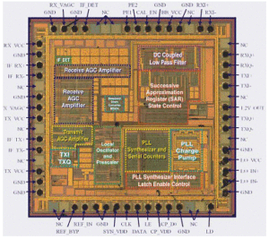
Recover MCU ATmega168PV Code
Recover MCU ATmega168PV Code from locked flash memory, fuse bit of microcontroller atmega168pv will be cracked and heximal file in the program and data memory will be extracted from chip atmega168pv;
An EEPROM data corruption can be caused by two situations when the voltage is too low. First, a regular write sequence to the EEPROM requires a minimum voltage to operate correctly. Secondly, the CPU itself can execute instructions incorrectly, if the supply voltage is too low when Recover MCU.
EEPROM data corruption can easily be avoided by following this design recommendation: Keep the AVR RESET active (low) during periods of insufficient power supply voltage. This can be done by enabling the internal Brown-out Detector (BOD). If the detection level of the internal BOD does not match the needed detection level, an external low VCC reset Protection circuit can be used if Recover MCU.
If a reset occurs while a write operation is in progress, the write operation will be completed provided that the power supply voltage is sufficient. The I/O space definition of the ATmega48/88/168 is shown in ”Register Summary” on page 342. All ATmega48/88/168 I/Os and peripherals are placed in the I/O space. All I/O locations may be accessed by the LD/LDS/LDD and ST/STS/STD instructions, transferring data between the 32 general purpose working registers and the I/O space. I/O Registers within the address range 0x00 – 0x1F are directly bit-accessible using the SBI and CBI instructions. In these registers, the value of single bits can be checked by using the SBIS and SBIC instructions before break atmega128pa MCU.
Refer to the instruction set section for more details. When using the I/O specific commands IN and OUT, the I/O addresses 0x00 – 0x3F must be used. When addressing I/O Registers as data space using LD and ST instructions, 0x20 must be added to these addresses. The ATmega48/88/168 is a complex MCU with more peripheral units than can be supported within the 64 location reserved in Opcode for the IN and OUT instructions.
For the Extended I/O space from 0x60 – 0xFF in SRAM, only the ST/STS/STD and LD/LDS/LDD instructions can be used. For compatibility with future devices, reserved bits should be written to zero if accessed. Reserved I/O memory addresses should never be written. Some of the Status Flags are cleared by writing a logical one to them. Note that, unlike most other AVRs, the CBI and SBI instructions will only operate on the specified bit, and can therefore be used on registers containing such Status Flags. The CBI and SBI instructions work with registers 0x00 to 0x1F only when break atmega168a MCU.
The I/O and peripherals control registers are explained in later sections. The ATmega48/88/168 contains three General Purpose I/O Registers. These registers can be used for storing any information, and they are particularly useful for storing global variables and Status Flags. General Purpose I/O Registers within the address range 0x00 – 0x1F are directly bit-accessible using the SBI, CBI, SBIS, and SBIC instructions.
The EEPROM Read Enable Signal EERE is the read strobe to the EEPROM. When the correct address is set up in the EEAR Register, the EERE bit must be written to a logic one to trigger the EEPROM read. The EEPROM read access takes one instruction, and the requested data is available immediately. When the EEPROM is read, the CPU is halted for four cycles before the next instruction is executed.
The user should poll the EEPE bit before starting the read operation. If a write operation is in progress, it is neither possible to read the EEPROM, nor to change the EEAR Register. The calibrated Oscillator is used to time the EEPROM accesses. Table 6-2 lists the typical programming time for EEPROM access from the CPU.
The following code examples show one assembly and one C function for writing to the EEPROM. The examples assume that interrupts are controlled (e.g. by disabling interrupts globally) so that no interrupts will occur during execution of these functions. The examples also assume that no Flash Boot Loader is present in the software. If such code is present, the EEPROM write function must also wait for any ongoing SPM command to finish when Recover MCU.
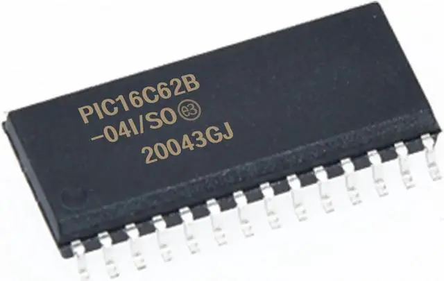
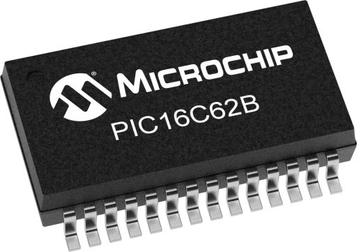
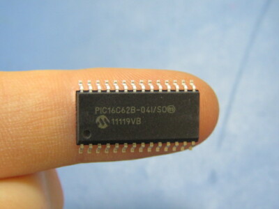
Recover Microcontroller PIC16C62B Eeprom
When a device relies on the Microchip PIC16C62B for control and configuration, the small but critical EEPROM and flash areas often hold calibration tables, configuration data, or archived program fragments that are essential to operation. Our service, searchable under the keyword Recover Microcontroller PIC16C62B Eeprom, helps authorized owners and technicians safely open, readout, restore, and duplicate the firmware/binary/heximal and small nonvolatile memory regions of these controllers. We focus on lawful, confidential recovery that returns usable program archives without disclosing methods to bypass manufacturer protections.
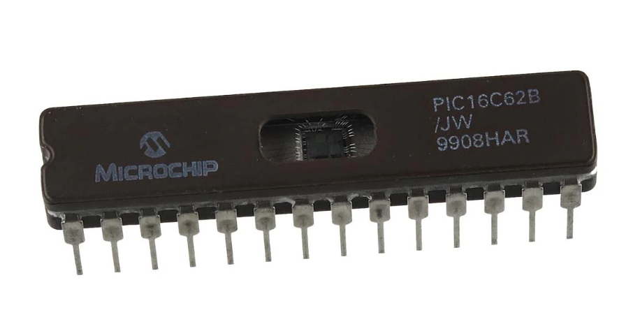
Recover Microcontroller PIC16C62B Eeprom data and extract mcu pic16c62b code from flash and eeprom memory, the secured firmware can be readount from mcu pic16c62b microprocessor memory;
We can recover MCU PIC16C62B Eeprom, please view the Microcontroller PIC16C62B features for your reference:
Microcontroller Core Features: · High-performance RISC CPU · Only 35 single word instructions to learn · All single cycle instructions except for program branches, which are two cycle·
Operating speed: DC – 20 MHz clock input DC – 200 ns instruction cycle · 2K x 14 words of Program Memory, 128 x 8 bytes of Data Memory (RAM) ·
Devices with PIC16C62B controllers are often legacy or long-lived products. Valid reasons to request recovery include the need to restore corrupted EEPROM after failures, copy configuration files for authorized spares, clone settings for production runs, or duplicate archived data before servicing. Recovering a verified binary or heximal image of the EEPROM can avoid lengthy software rewrites and shorten downtime.
Typical applications of PIC16C62B
The PIC16C62B’s modest feature set and reliable I/O make it suitable for many industries:
- Consumer appliances and simple household electronics.
- Industrial sensors and controllers for basic automation tasks.
- Instrumentation and measurement devices that store small data archives.
- Aftermarket and hobbyist systems where a compact embedded controller is sufficient.
Because these applications frequently store system-critical parameters in EEPROM, the data is often treated as a protected, locked, or secured asset.
Eight level deep hardware stack ·
Direct, indirect, and relative addressing modes ·
Power-on Reset (POR) · Power-up Timer (PWRT) and Oscillator Start-up Timer (OST)·
Watchdog Timer (WDT) with its own on-microcontroller RC oscillator for reliable operation · Brown-out detection circuitry for Brown-out Reset (BOR) · Programmable code-protection · Power saving SLEEP mode · Selectable oscillator options · Low-power, high-speed CMOS EPROM technology·
Fully static design · In-Circuit Serial Programming (ICSP) · Wide operating voltage range: 2.5V to 5.5V · High Sink/Source Current 25/25 mA · Commercial, Industrial and Extended temperature ranges · Low-power consumption: – < 2 mA @ 5V, 4 MHz – 22.5 µA typical @ 3V, 32 kHz when copy pic16f684 Microcontroller firmware – < 1 µA typical standby current Peripheral Features: · Timer0: 8-bit timer/counter with 8-bit prescaler · Timer1: 16-bit timer/counter with prescaler, can be incremented during sleep via external crystal/clock · Timer2: 8-bit timer/counter with 8-bit period register, prescaler and postscaler · Capture, Compare, PWM module · Capture is 16-bit, max. resolution is 12.5 ns, Compare is 16-bit, max. resolution is 200 ns, PWM maximum resolution is 10-bit · 8-bit multi-channel Analog-to-Digital converter · Synchronous Serial Port (SSP) with Enhanced SPI and I2C
The PIC16C62B integrates limited program memory alongside EEPROM for persistent settings, plus basic analog/digital peripherals. These constrained resources mean key configuration files and calibration tables are concentrated in small memory regions — making careful extraction essential. The chip’s architecture affects how source code (if available) and program data are represented in the raw binary/heximal dumps.
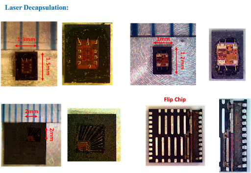
General idea of our approach (non-actionable)
We begin every engagement with ownership verification and a risk assessment. Our work emphasizes non-destructive procedures to obtain a reliable memory archive. After a validated readout, we produce checked heximal or binary dumps and provide high-level annotated summaries that help engineers interpret recovered data. We do not publish or provide step-by-step techniques to crack, hack, or illegally decode protections — our focus is on authorized recovery, unlock, and restoration for legitimate purposes.
Purpose and benefits for end users
Clients using this service can expect faster recovery of device functionality, secure backups of previously inaccessible EEPROM, and the ability to copy or clone settings for authorized production or maintenance. Recovered program files and archives support debugging, testing, migration to replacement hardware, and continuity for legacy systems — saving time and reducing redevelopment costs.
Common difficulties and limitations
Challenges may include partial data corruption, variant device revisions with different memory maps, or layered protective settings that limit full reconstruction. In many recoveries, the deliverable is a validated binary/heximal archive and assembly-level annotations rather than full, human-readable source code. We always communicate feasibility, likely outcomes, and limitations before proceeding.
Ethics, authorization & confidentiality
All projects require proof of ownership or explicit authorization and are governed by confidentiality agreements. We do not assist with unauthorized copying or distribution of copyrighted or safety-critical firmware. Our goal is to help rightful owners recover, restore, and maintain their embedded systems safely and legally.
If you need to Recover Microcontroller PIC16C62B Eeprom for authorized recovery, maintenance, or archival purposes, our experienced team offers secure, professional support to retrieve and document your embedded firmware and data while protecting your IP and operational continuity.
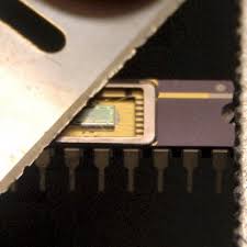
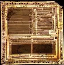
Extract Chip PIC16C57 Heximal File
Extract Chip PIC16C57 Heximal File from flash memory, original programmed MCU pic16c57 will be readout and program/data from flash/eeprom of microcontroller pic16c57 can be duplicated;
A fetch cycle begins with the program counter (PC) incrementing in Q1. In the execution cycle, the fetched instruction is latched into the Instruction Register (IR) in cycle Q1.
This instruction is then decoded and executed during the Q2, Q3, and Q4 cycles. Data memory is extract during Q2 (operand extract) and written during Q4 (destination write) if recover pic16c554 memory software.
All instructions are single cycle, except for any program branches. These take two cycles since the fetch instruction is “flushed” from the pipeline while the new instruction is being fetched and then executed.
PIC16C57 memory is organized into program memory and data memory. For devices with more than 512 bytes of program memory, a paging scheme is used after recover microcontroller pic16f83 eeprom.
Program memory pages are accessed using one STATUS register bit. For the PIC16C57 with a data memory register file of more than 32 registers, a banking scheme is used.
Data memory banks are accessed using the File Select Register (FSR). The PIC16C57 devices have a 12-bit Program Counter (PC) capable of addressing a 2K x 12 program memory space. Only the first 512 x 12 (0000h-01FFh) for the PIC16C57 and 1K x 12 (0000h-03FFh) for the PIC16C57 are physically implemented before copy epm9320arc208 cpld jed file.
Refer to Figure 4-1. Accessing a location above these boundaries will cause a wrap around within the first 512 x 12 space (PIC16C57) or 1K x 12 space (PIC16C57).
The effective reset vector is at 000h, (see Figure 4-1). Location 01FFh (PIC16C57) or location 03FFh (PIC16C57) contains the internal clock oscillator calibration value. This value should never be overwritten.
Open Microcontroller PIC12LC509A Security bits
Open Microcontroller PIC12LC509A and extract embedded firmware from mcu pic12lc509a flash memory, Security bits will be decrypted to disable the protection on the microprocessor 12lc509a;
Microchip offers a unique programming service where a few user-defined locations in each device are programmed with different serial numbers when recover microcontroller stm32f105rct6 binary.
The serial numbers may be random, pseudo-random or sequential. Serial programming allows each device to have a unique number which can serve as an entry-code, password or ID number.
The high performance of the PIC12C5XX family can be attributed to a number of architectural features commonly found in RISC microprocessors.
To begin with, the PIC12C5XX uses a Harvard architecture in which program and data are accessed on separate buses. This improves bandwidth over traditional von Neumann architecture where program and data are fetched on the same bus.
Separating program and data memory further allows instructions to be sized differently than the 8-bit wide data word. Instruction opcodes are 12-bits wide making it possible to have all single word instructions when break microcontroller atmega128 heximal.
A 12-bit wide program memory access bus fetches a 12-bit instruction in a single cycle. A two-stage pipeline overlaps fetch and execution of instructions. Consequently, all instructions (33) execute in a single cycle (1µs @ 4MHz) except for program branches.
The table below lists program memory (EPROM), data memory (RAM), ROM memory, and non-volatile (EEPROM) for each device.
The PIC12C5XX can directly or indirectly address its register files and data memory. All special function registers including the program counter are mapped in the data memory. The PIC12C5XX has a highly orthogonal (symmetrical) instruction set that makes it possible to carry out any operation on any register using any addressing mode.
This symmetrical nature and lack of ‘special optimal situations’ make programming with the PIC12C5XX simple yet efficient. In addition, the learning curve is reduced significantly.