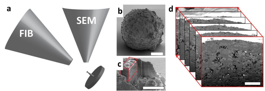
Archive for the ‘Recover Chip’ Category
 Recover IC PIC12LC508A Eeprom
Recover IC PIC12LC508A Eeprom needs to unlock mcu pic12lc508a protection and then extract the firmware from microcontroller pic12lc508a flash and eeprom memory;
A variety of packaging options are available. Depending on application and production requirements, the proper device option can be selected using the information in this section.
When placing orders, please use the PIC12C5XX Product Identification System at the back of this data sheet to specify the correct part number if copy mcu pic16c554a eeprom.
The UV erasable version, offered in ceramic side brazed package, is optimal for prototype development and pilot programs. before production shipments are available. Please contact your local Microchip Technology sales office for more details.
The UV erasable version can be erased and reprogrammed to any of the configuration modes.
Note: Please note that erasing the device will also erase the pre-programmed internal calibration value for the internal oscillator after copy microcontroller pic16c76 hex.
The calibration value must be saved prior to erasing the part. Microchip’s PICSTART® PLUS and PRO MATE® programmers all support programming of the PIC12C5XX.
Third party programmers also are available;
Microchip Third Party Guide for a list of sources. The availability of OTP devices is especially useful for customers who need the flexibility for frequent eeprom updates or small volume applications.
The OTP devices, packaged in plastic packages permit the user to program them once. In addition to the program memory, the configuration bits must also be programmed before Recover IC atmega64l eeprom.
Microchip offers a QTP Programming Service for factory production orders. This service is made available for users who choose not to program a medium to high quantity of units and whose eeprom patterns have stabilized.
The devices are identical to the OTP devices but with all EPROM locations and fuse options already programmed by the factory. Certain eeprom and prototype verification procedures do apply before production shipments are available.
Copying Chip PIC12LF510 Program
Copying Chip PIC12LF510 Program from flash memory, the secured microcontroller will be unlocked and readout the embedded firmware heximal file from mcu pic12lf510;
The PICkit™ 2 Development Programmer is a low-cost programmer with an easy-to-use interface for programming many of Microchip’s baseline, mid-range and PIC18F families of Flash memory.
The PICkit 2 Starter Kit includes a prototyping development board, twelve sequential lessons, software and HI-TECH’s PICC™ Lite C compiler, and is designed to help get up to speed quickly using PIC® copying dsp mcu tms320lf2401avfa program.
The kit provides everything needed to program, evaluate and develop applications using Microchip’s powerful, mid-range Flash memory family of chip copying.
A wide variety of demonstration, development and evaluation boards for various PIC MCUs and dsPIC DSCs allows quick application development on fully functional systems if Copying microcontroller pic16c711 firmware.
Most boards include prototyping areas for adding custom circuitry and provide application firmware and source code for examination and modification.
The boards support a variety of features, including LEDs, temperature sensors, switches, speakers, RS-232 interfaces, LCD displays, potentiometers and additional EEPROM memory.
The demonstration and development boards can be used in teaching environments, for prototyping custom circuits and for learning about various chip applications after recover mcu pic16c73b firmware.
In addition to the PICDEM™ and dsPICDEM™ demonstration/development board series of circuits, Microchip has a line of evaluation kits and demonstration software for analog filter design, KEELOQ® security ICs, CAN, IrDA®, PowerSmart® battery management, SEEVAL® evaluation system, Sigma-Delta ADC, flow rate sensing, plus many more.
Check the Microchip web page (www.microchip.com) and the latest “Product Selector Guide” (DS00148) for the complete list of demonstration, development and evaluation kits.
Recover IC ATmega8PA Firmware
Recover IC ATmega8PA Firmware from embedded flash and eeprom memory, the secured firmware data can be readout from atmega8pa memory, crack atmega8pa protective system by removing the security fuse bit;
The AVR core combines a rich instruction set with 32 general purpose working registers. All the 32 registers are directly connected to the Arithmetic Logic Unit (ALU), allowing two independent registers to be accessed in one single instruction executed in one clock cycle.
The resulting architecture is more code efficient while achieving throughputs up to ten times faster than conventional CISC microcontrollers. The ATmega8 provides the following features: 8K bytes of In-System Programmable Flash with Recover-While-Write capabilities, 512 bytes of EEPROM, 1K byte of SRAM, 23 general purpose I/O lines, 32 general purpose working registers, three flexible Timer/Counters with compare modes if Recover IC, internal and external interrupts, a serial programmable USART, a byte oriented Two-wire Serial Interface, a 6-channel ADC (eight channels in TQFP and QFN/MLF packages) with 10-bit accuracy, a programmable Watchdog Timer with Internal Oscillator, an SPI serial port, and five software selectable power saving modes before Reading avr chip embedded firmware.
The Idle mode stops the CPU while allowing the SRAM, Timer/Counters, SPI port, and interrupt system to continue functioning. The Power-down mode saves the register contents but freezes the Oscillator, disabling all other chip functions until the next Interrupt or Hardware Reset.
In Power-save mode, the asynchronous timer continues to run, allowing the user to maintain a timer base while the rest of the device is sleeping. The ADC Noise Reduction mode stops the CPU and all I/O modules except asynchronous timer and ADC, to minimize switching noise during ADC conversions.
In Standby mode, the crystal/resonator Oscillator is running while the rest of the device is sleeping. This allows very fast start-up combined with low-power consumption. The device is manufactured using Atmel’s high density non-volatile memory technology.
The Flash Program memory can be reprogrammed In-System through an SPI serial interface, by a conventional non-volatile memory programmer, or by an On-chip boot program running on the AVR core. The boot program can use any interface to download the application program in the Application Flash memory.
Software in the Boot Flash Section will continue to run while the Application Flash Section is updated, providing true Recover-While-Write operation. By combining an 8-bit RISC CPU with In-System Self Programmable Flash on a monolithic chip, the Atmel ATmega8 is a powerful microcontroller that provides a highly-flexible and cost-effective solution to many embedded control applications.
The ATmega8 AVR is supported with a full suite of program and system development tools, including C compilers, macro assemblers, program debugger/simulators, In-Circuit Emulators, and evaluation kits.
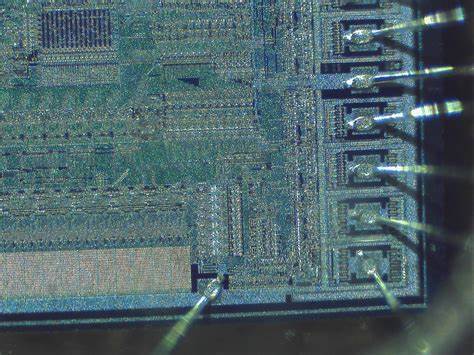
Reverse Chip PIC12LC508 Heximal File
Reverse Chip PIC12LC508 Heximal File is a process to replicate cpu pic12lf508 program from memory, and then extract the code from pic12lf508 locked flash memory.
A serial frame for the MSPIM is defined to be one character of 8 data bits. The USART in MSPIM mode has two valid frame formats:
8-bit data with MSB first
8-bit data with LSB first
A frame starts with the least or most significant data bit. Then the next data bits, up to a total of eight, are succeeding, ending with the most or least significant bit accordingly when attack mcu aduc831bsz firmware Heximal file.
When a complete frame is transmitted, a new frame can directly follow it, or the communication line can be set to an idle (high) state.
The UDORDn bit in UCSRnC sets the frame format used by the USART in MSPIM mode. The Receiver and Transmitter use the same setting. Note that changing the setting of any of these bits will corrupt all ongoing communication for both the Receiver and Transmitter before attack mcu tms320f28027pta CHIP.
16-bit data transfer can be achieved by writing two data bytes to UDRn. A UART transmit complete interrupt will then signal that the 16-bit value has been shifted out.
The USART in MSPIM mode has to be initialized before any communication can take place. The initialization process normally consists of setting the baud rate, setting master mode of operation (by setting DDR_XCKn to one), setting frame format and enabling the Transmitter and the Receiver.
Only the transmitter can operate independently. For interrupt driven USART operation, the Global Interrupt Flag should be cleared (and thus interrupts globally disabled) when doing the initialization.
Note:
To ensure immediate initialization of the XCKn output the baud-rate register (UBRRn) must be zero at the time the transmitter is enabled.
Contrary to the normal mode USART operation the UBRRn must then be written to the desired value after the transmitter is enabled, but before the first transmission is started after copy pic16lf877 program.
Setting UBRRn to zero before enabling the transmitter is not necessary if the initialization is done immediately after a reset since UBRRn is reset to zero.
Before doing a re-initialization with changed baud rate, data mode, or frame format, be sure that there is no ongoing transmissions during the period the registers are changed if copy mcu pic18f2480 program.
The TXCn Flag can be used to check that the Transmitter has completed all transfers, and the RXCn Flag can be used to check that there are no unread data in the receive buffer.
Note that the TXCn Flag must be cleared before each transmission (before UDRn is written) if it is used for this purpose. The following simple USART initialization heximal file examples show one assembly and one C function that are equal in functionality.
The examples assume polling (no interrupts enabled). The baud rate is given as a function parameter. For the assembly heximal file, the baud rate parameter is assumed to be stored in the r17:r16 registers.
Open IC PIC16C52 Program
Open IC PIC16C52 and unlock mcu pic16c52 flash memory, extract embedded Program from microcontroller pic16c52 flash and eeprom memory in the format of heximal or binary;
This bit is set if the next character in the receive buffer had a Frame Error when received. I.e., when the first stop bit of the next character in the receive buffer is zero.
This bit is valid until the receive buffer (UDRn) is read. The FEn bit is zero when the stop bit of received data is one. Always set this bit to zero when writing to UCSRnA. This bit is set if a Data OverRun condition is detected. A Data OverRun occurs when the receive buffer is full (two characters), it is a new character waiting in the Receive Shift Register, and a new start bit is detected.
This bit is valid until the receive buffer (UDRn) is read. Always set this bit to zero when writing to UCSRnA. This bit is set if the next character in the receive buffer had a Parity Error when received and the Parity Checking was enabled at that point (UPMn1 = 1).
This bit is valid until the receive buffer (UDRn) is read. Always set this bit to zero when writing to UCSRnA. This bit only has effect for the asynchronous operation. Write this bit to zero when using synchronous operation when copy pic16f886 IC firmware program.
Writing this bit to one will reduce the divisor of the baud rate divider from 16 to 8 effectively doubling the transfer rate for asynchronous communication. This bit enables the Multi-processor Communication mode.
When the MPCMn bit is written to one, all the incoming frames received by the USART Receiver that do not contain address information will be ignored. The Transmitter is unaffected by the MPCMn setting. For more detailed information see “Multi-processor Communication Mode” on page 221. Writing this bit to one enables interrupt on the RXCn Flag. A USART Receive Complete interrupt will be generated only if the RXCIEn bit is written to one, the Global Interrupt Flag in SREG is written to one and the RXCn bit in UCSRnA is set after attack mcu atmega162 flash memory.
Writing this bit to one enables interrupt on the TXCn Flag. A USART Transmit Complete interrupt will be generated only if the TXCIEn bit is written to one, the Global Interrupt Flag in SREG is written to one and the TXCn bit in UCSRnA is set.
Writing this bit to one enables interrupt on the UDREn Flag. A Data Register Empty interrupt will be generated only if the UDRIEn bit is written to one, the Global Interrupt Flag in SREG is written to one and the UDREn bit in UCSRnA is set after attack chip pic16f72 memory.
Recovery Chip PIC16C505 Eeprom
Recovery Chip PIC16C505 Eeprom content needs to crack pic16c505 mcu protection and extract embedded firmware from microcontroller pic16c505;
The USART Transmit Data Buffer Register and USART Receive Data Buffer Registers share the same I/O address referred to as USART Data Register or UDRn. The Transmit Data Buffer Register (TXB) will be the destination for data written to the UDRn Register location.
Reading the UDRn Register location will return the contents of the Receive Data Buffer Register (RXB). For 5-, 6-, or 7-bit characters the upper unused bits will be ignored by the Transmitter and set to zero by the Receiver if copy microcontroller p87c51x2bbd.
The transmit buffer can only be written when the UDREn Flag in the UCSRnA Register is set. Data written to UDRn when the UDREn Flag is not set, will be ignored by the USART Transmitter.
When data is written to the transmit buffer, and the Transmitter is enabled, the Transmitter will load the data into the Transmit Shift Register when the Shift Register is empty. Then the data will be serially transmitted on the TxDn pin. The receive buffer consists of a two level FIFO. The FIFO will change its state whenever the receive buffer is accessed. Due to this behavior of the receive buffer, do not use Read-Modify-Write instructions (SBI and CBI) on this location if Recovery mcu pic18f2520 bin.
Be careful when using bit test instructions (SBIC and SBIS), since these also will change the state of the FIFO. This flag bit is set when there are unread data in the receive buffer and cleared when the receive buffer is empty (i.e., does not contain any unread data).
If the Receiver is disabled, the receive buffer will be flushed and consequently the RXCn bit will become zero. The RXCn Flag can be used to generate a Receive Complete interrupt (see description of the RXCIEn bit) before Recovery Chip mc68hc11a0fn3 binary.
This flag bit is set when the entire frame in the Transmit Shift Register has been shifted out and there are no new data currently present in the transmit buffer (UDRn). The TXCn Flag bit is automatically cleared when a transmit complete interrupt is executed, or it can be cleared by writing a one to its bit location. The TXCn Flag can generate a Transmit Complete interrupt (see description of the TXCIEn bit).
The UDREn Flag indicates if the transmit buffer (UDRn) is ready to receive new data. If UDREn is one, the buffer is empty, and therefore ready to be written. The UDREn Flag can generate a Data Register Empty interrupt (see description of the UDRIEn bit). UDREn is set after a reset to indicate that the Transmitter is ready.
Recover Chip PIC12C509A Firmware
Recover Chip PIC12C509A Firmware from embedded memory, the program and data can be extracted from pic12c509a mcu and read out from secured microcontroller pic12c509a memory;
The same majority voting is done to the stop bit as done for the other bits in the frame. If the stop bit is registered to have a logic 0 value, the Frame Error (FEn) Flag will be set.
A new high to low transition indicating the start bit of a new frame can come right after the last of the bits used for majority voting. For Normal Speed mode, the first low level sample can be at point marked (A) in Figure 89 if Recover mcu stm32f107rct6 code firmware.
For Double Speed mode the first low level must be delayed to (B). (C) marks a stop bit of full length. The early start bit detection influences the operational range of the Receiver.
The operational range of the Receiver is dependent on the mismatch between the received bit rate and the internally generated baud rate after copy microcontroller pic16f684 memory.
If the Transmitter is sending frames at too fast or too slow bit rates, or the internally generated baud rate of the Receiver does not have a similar (see Table 99) base frequency, the Receiver will not be able to synchronize the frames to the start bit.
The following equations can be used to calculate the ratio of the incoming data rate and internal receiver baud rate. Sum of character size and parity size (D = 5 to 10 bit) Samples per bit. S = 16 for Normal Speed mode and S = 8 for Double Speed mode.
First sample number used for majority voting. SF = 8 for normal speed and SF = 4 for Double Speed mode. Middle sample number used for majority voting.
SM = 9 for normal speed and
SM = 5 for Double Speed mode.
Rslow is the ratio of the slowest incoming data rate that can be accepted in relation to the receiver baud rate. Rfast is the ratio of the fastest incoming data rate that can be accepted in relation to the receiver baud rate. Table 99 and Table 100 list the maximum receiver baud rate error that can be tolerated. Note that Normal Speed mode has higher toleration of baud rate variations after extract mcu pic16f54c hex.
Recovery IC PIC16F54C Program
Recovery IC PIC16F54C Program from its locked flash memory, crack mcu pic16f54c flash memory and extract locked heximal microcontroller pic16f54c;
The USART Receiver has three Error Flags: Frame Error (FEn), Data OverRun (DORn) and Parity Error (UPEn). All can be accessed by reading UCSRnA. Common for the Error Flags is that they are located in the receive buffer together with the frame for which they indicate the error status.
Due to the buffering of the Error Flags, the UCSRnA must be read before the receive buffer (UDRn), since reading the UDRn I/O location changes the buffer read location. Another equality for the Error Flags is that they can not be altered by software doing a write to the flag location. However, all flags must be set to zero when the UCSRnA is written for upward compatibility of future USART implementations after Reverse mcu atmega461pv binary.
None of the Error Flags can generate interrupts. The Frame Error (FEn) Flag indicates the state of the first stop bit of the next readable frame stored in the receive buffer.
The FEn Flag is zero when the stop bit was correctly read (as one), and the FEn Flag will be one when the stop bit was incorrect (zero). This flag can be used for detecting out-of-sync conditions, detecting break conditions and protocol handling.
The FEn Flag is not affected by the setting of the USBSn bit in UCSRnC since the Receiver ignores all, except for the first, stop bits. For compatibility with future devices, always set this bit to zero when writing to UCSRnA before break atmega461p IC flash.
The Data OverRun (DORn) Flag indicates data loss due to a receiver buffer full condition. A Data OverRun occurs when the receive buffer is full (two characters), it is a new character waiting in the Receive Shift Register, and a new start bit is detected.
If the DORn Flag is set there was one or more serial frame lost between the frame last read from UDRn, and the next frame read from UDRn. For compatibility with future devices, always write this bit to zero when writing to UCSRnA. The DORn Flag is cleared when the frame received was successfully moved from the Shift Register to the receive buffer.
The Parity Error (UPEn) Flag indicates that the next frame in the receive buffer had a Parity Error when received. If Parity Check is not enabled the UPEn bit will always be read zero. For compatibility with future devices, always set this bit to zero when writing to UCSRnA. For more details see “Parity Bit Calculation” on page 210 and “Parity Checker”.
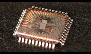
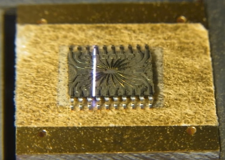
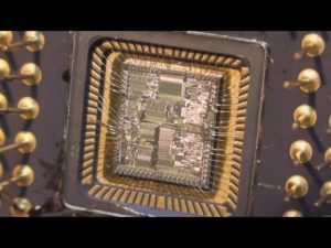
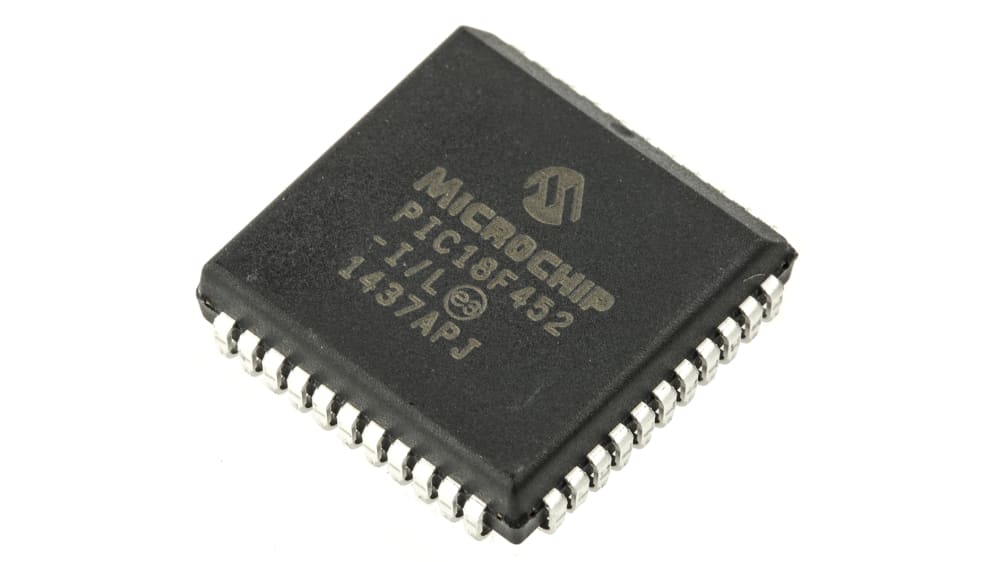
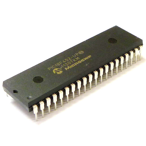
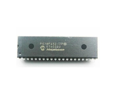
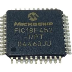
Recover MCU PIC18F452 Program
When embedded systems fail, are upgraded, or require inspection, access to the original firmware can be vital. Our service — summarized under the keyword Recover MCU PIC18F452 Program — helps legitimate owners and authorized technicians restore, readout, copy, clone, or duplicate the protected program held inside Microchip’s PIC18F452 MCU. We focus on recovering the firmware/binary/heximal image and producing usable outputs while respecting legal and ethical boundaries.
Recover MCU PIC18F452 Program starts from unlocking microcontroller pic18f452 secured memory and extract pic18f452 secured flash memory content;
A “fast interrupt return” option is available for interrupts. A Fast Register Stack is provided for the STATUS, WREG and BSR registers and are only one in depth. The stack is not recoverable or writable and is loaded with the current value of the corresponding register when the processor vectors for an interrupt. The values in the registers are then loaded back into the working registers, if the FAST RETURN instruction is used to return from the interrupt.
A low or high priority interrupt source will push values into the stack registers. If both low and high priority interrupts are enabled, the stack registers cannot be used reliably for low priority interrupts. If a high priority interrupt occurs while servicing a low priority interrupt, the stack register values stored by the low priority interrupt will be overwritten if break pic12f635 MCU program.
Why clients need PIC18F452 program recovery
The PIC18F452 is a workhorse in many legacy and modern applications thanks to its flexible I/O, analog and timing peripherals, and on-chip nonvolatile memories. Devices built around this MCU often contain essential program files, calibration data, and archived memory that control hardware behavior. Typical reasons to request recovery include:
- Restore a device after accidental corruption or bad firmware updates.
- Duplicate/clone firmware for manufacturing spares or supporting legacy production.
- Migrate software to replacement hardware during end-of-life transitions.
- Audit or validate embedded code for safety, compliance, or forensic analysis.
What we do (high level, non-invasive)
Our service helps customers to legally open, unlock, decode, and extract the embedded flash/eeprom contents without publishing methods to bypass manufacturer protections. Key outcomes include:
- Verified extraction of the raw binary/heximal firmware image.
- Data integrity checks and documented checksums for recovery traceability.
- High-level decoding and annotated disassembly to aid engineers in understanding the recovered code.
- Delivery of recoverable files and a concise recovery report describing what was found and recommended next steps.
We do not provide procedural guidance to circumvent protections for unlawful purposes. All projects require proof of ownership or explicit authorization.
If high priority interrupts are not disabled during low priority interrupts, users must save the key registers in software during a low priority interrupt. If no interrupts are used, the fast register stack can be used to restore the STATUS, WREG and BSR registers at the end of a subroutine call. To use the fast register stack for a subroutine call, a FAST CALL instruction must be executed.
Example 4-1 shows a source code example that uses the fast register stack. The program counter (PC) specifies the address of the instruction to fetch for execution. The PC is 21-bits wide. The low byte is called the PCL register. This register is recoverable and writable. The high byte is called the PCH register. This register contains the PC<15:8> bits and is not directly recoverable or writable after break pic12f629 MCU program.
Updates to the PCH register may be performed through the PCLATH register. The upper byte is called PCU. This register contains the PC<20:16> bits and is not directly recoverable or writable. Updates to the PCU register may be performed through the PCLATU register.
The PC addresses bytes in the program memory. To prevent the PC from becoming misaligned with word instructions, the LSB of PCL is fixed to a value of ’0’. The PC increments by 2 to address sequential instructions in the program memory.
The CALL, RCALL, GOTO and program branch instructions write to the program counter directly. For these instructions, the contents of PCLATH and PCLATU are not transferred to the program counter.
Applications where PIC18F452 matters
The PIC18F452’s blend of digital control and analog support makes it common across multiple industries:
- Industrial controllers and instrumentation, where deterministic timing and ADCs matter.
- Consumer electronics and appliances, for feature logic and user interfaces.
- Automotive subsystems in legacy modules that use robust 8-bit control.
- Medical instruments and test equipment that rely on stable, well-tested firmware.
Because these systems often run long past their original support window, firmware recovery is frequently the only path to safe maintenance, calibration, or legal continuity.
Unique recovery considerations for PIC18F452
The PIC18F family commonly stores program code in on-chip flash with supplementary EEPROM for parameter data. Firmware may be protected, locked, or use custom bootloader schemes that complicate straightforward readout. Our approach combines careful chip identification, non-destructive readout methods, and conservative validation to minimize the risk of data loss. We prioritize preserving the device and its memory contents while delivering actionable artifacts to the customer.
The contents of PCLATH and PCLATU will be transferred to the program counter by an operation that writes PCL. Similarly, the upper two bytes of the program counter will be transferred to PCLATH and PCLATU by an operation that recovers PCL. This is useful for computed offsets to the PC.
The clock input (from OSC1) is internally divided by four to generate four non-overlapping quadrature clocks, namely Q1, Q2, Q3 and Q4. Internally, the program counter (PC) is incremented every Q1, the instruction is fetched from the program memory and latched into the instruction register in Q4.
The instruction is decoded and executed during the following Q1 through Q4. The clocks and instruction execution flow are shown in Figure 4-4. An “Instruction Cycle” consists of four Q cycles (Q1, Q2, Q3 and Q4). The instruction fetch and execute are pipelined such that fetch takes one instruction cycle, while decode and execute takes another instruction cycle;
However, due to the pipelining, each instruction effectively executes in one cycle. If an instruction causes the program counter to change (e.g., GOTO) then two cycles are required to complete the instruction (Example 4-2). The program memory is addressed in bytes. Instructions are stored as two bytes or four bytes in program memory.
The Least Significant Byte of an instruction word is always stored in a program memory location with an even address (LSB =’0’). Figure 4-5 shows an example of how instruction words are stored in the program memory. To maintain alignment with instruction boundaries, the PC increments in steps of 2 and the LSB will always recover ’0’ (see Section 4.4).
Clients receive the recovered heximal/binary file, a recovery certificate, and optional annotated disassembly to support debugging, porting, or re-engineering. Every engagement is governed by confidentiality agreements and an authorization check — our commitment is to lawful, ethical recovery for repair, backup, migration, or authorized analysis.
If you need to Recover MCU PIC18F452 Program — to restore, clone, or recover crucial program archives from a protected or secured device — our team provides secure, professional support that safeguards your data and operational continuity.
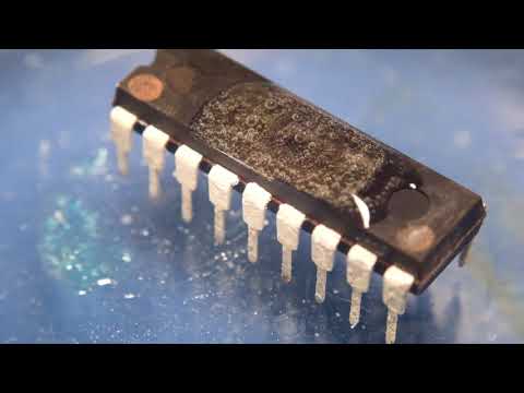
Recover Microcontroller PIC18F252 Program
Recover Microcontroller PIC18F252 Program means the embedded heximal of mcu pic18f252 will be copied out from original flash memory after cracking protected mcu pic18f252.
Recover Microcontroller PIC18F252 Program means the embedded heximal of mcu pic18f252 will be copied out from original flash memory after cracking protected mcu pic18f252
CMOS Technology:
· Low power, high speed FLASH/EEPROM technology
· Fully static design
· Wide operating voltage range (2.0V to 5.5V)
· Industrial and Extended temperature ranges
· Low power consumption:
– < 1.6 mA typical @ 5V, 4 MHz
– 25 ìA typical @ 3V, 32 kHz
– < 0.2 ìA typical standby current
For timing-insensitive applications, the “RC” and “RCIO” device options offer additional cost savings.
The RC oscillator frequency is a function of the supply voltage, the resistor (REXT) and capacitor (CEXT) values and the operating temperature. In addition to this, the oscillator frequency will vary from unit to unit due to normal process parameter variation before copying pic16f627a microcontroller.
Furthermore, the difference in lead frame capacitance between package types will also affect the oscillation frequency, especially for low CEXT values. The user also needs to take into account variation due to tolerance of external R and C components used. Figure 2-3 shows how the R/C combination is connected.
In the RC Oscillator mode, the oscillator frequency divided by 4 is available on the OSC2 pin. This signal may be used for test purposes or to synchronize other logic.
The RCIO Oscillator mode functions like the RC mode, except that the OSC2 pin becomes an additional general purpose I/O pin. The I/O pin becomes bit 6 of PORTA (RA6).
The EC and ECIO Oscillator modes require an external clock source to be connected to the OSC1 pin. The feedback device between OSC1 and OSC2 is turned off in these modes to save current. There is no oscillator start-up time required after a Power-on Reset or after a recovery from SLEEP mode.
In the EC Oscillator mode, the oscillator frequency divided by 4 is available on the OSC2 pin. This signal may be used for test purposes or to synchronize other logic. Figure 2-4 shows the pin connections for the EC Oscillator mode.