Archive for the ‘Recover Chip’ Category
 Reverse Engineering Encrypted AVR Chip ATtiny261 Software
 January 22nd, 2012 |
  Author:
 We can Reverse Engineering Encrypted AVR Chip ATtiny261 Software, please view the AVR Chip ATtiny261 features for your reference:
The ATtiny261 is a low-power CMOS 8-bit encrypted AVR chip based on the AVR enhanced RISC architecture. By executing powerful instructions in a single clock cycle.
The ATtiny261 achieves throughputs approaching 1 MIPS per MHz allowing the system designer to optimize power consumption versus processing speed.
The AVR core combines a rich instruction set with 32 general purpose working registers. All the 32 registers are directly connected to the Arithmetic Logic Unit (ALU), allowing two independent registers to be accessed in one single instruction executed in one clock cycle before Reverse Engineering Encrypted AVR Chip ATtiny261 Software.
The resulting architecture is more code efficient while achieving throughputs up to ten times faster than conventional CISC encrypted AVR chips.
The ATtiny261 provides the following features: 2/4/8K byte of In-System Programmable Flash, 128/256/512 bytes EEPROM, 128/256/512 bytes SRAM, 6 general purpose I/O lines, 32 general purpose working registers, one 8-bit Timer/Counter with compare modes.
One 8-bit high speed Timer/Counter, Universal Serial Interface, Internal and External Interrupts, a 4-channel, 10-bit ADC, a programmable Watchdog Timer with internal Oscillator.
And three software selectable power saving modes. The Idle mode stops the CPU while allowing the SRAM, Timer/Counter, ADC, Analog Comparator, and Interrupt system to continue functioning before Reverse Engineering Encrypted AVR Chip ATtiny261 Software.
The Power-down mode saves the register contents, disabling all chip functions until the next Interrupt or Hardware Reset. The ADC Noise Reduction mode stops the CPU and all I/O modules except ADC, to minimize switching noise during ADC conversions.
The device is manufactured using Atmel’s high density non-volatile memory technology. The On-chip ISP Flash allows the Program memory to be re-programmed In-System through an SPI serial interface, by a conventional non-volatile memory programmer or by an On-chip boot code running on the AVR core when reverse engineering microcontroller.
Reverse Engineering IC ATmega1284PV Firmware
Reverse Engineering IC ATmega1284PV structure to locate the security fuse bit, by unlocking MCU ATmega1284 memory and readout ATmega1284 IC Firmware.
Timer/Counter0 is a general purpose 8-bit Timer/Counter module, with two independent Output Compare Units, and with PWM support. It allows accurate program execution timing (event management) and wave generation. The main features are:
Two Independent Output Compare Units
Double Buffered Output Compare Registers
Clear Timer on Compare Match (Auto Reload)
Glitch Free, Phase Correct Pulse Width Modulator (PWM)
Variable PWM Period
Frequency Generator
Three Independent Interrupt Sources (TOV0, OCF0A, and OCF0B)
A simplified block diagram of the 8-bit Timer/Counter is shown in Figure 38. For the actual placement of I/O pins, refer to “Pinout ATmega640/1280/2560” on page 2. CPU accessible I/O Registers, including I/O bits and I/O pins, are shown in bold. The device-specific I/O Register and bit locations are listed in the “8-bit Timer/Counter Register Description” on page 128.
The Timer/Counter (TCNT0) and Output Compare Registers (OCR0A and OCR0B) are 8-bit registers. Interrupt request (abbreviated to Int.Req. in the figure) signals are all visible in the Timer Interrupt Flag Register (TIFR0). All interrupts are individually masked with the Timer Interrupt Mask Register (TIMSK0). TIFR0 and TIMSK0 are not shown in the figure.
The Timer/Counter can be clocked internally, via the prescaler, or by an external clock source on the T0 pin. The Clock Select logic block controls which clock source and edge the Timer/Counter uses to increment (or decrement) its value when attack mcu pic16c558 program.
The Timer/Counter is inactive when no clock source is selected. The output from the Clock Select logic is referred to as the timer clock (clkT0).
The double buffered Output Compare Registers (OCR0A and OCR0B) are compared with the Timer/Counter value at all times. The result of the compare can be used by the Waveform Generator to generate a PWM or variable frequency output on the Output Compare pins (OC0A and OC0B). See “Output Compare Unit” on page 119. for details.
The Compare Match event will also set the Compare Flag (OCF0A or OCF0B) which can be used to generate an Output Compare interrupt request.
 Posted in Recover Chip |
  Tags: Reverse Engineering IC encrypted archive, Reverse Engineering IC encrypted binary, Reverse Engineering IC encrypted code, Reverse Engineering IC encrypted content, Reverse Engineering IC encrypted data, Reverse Engineering IC encrypted eeprom, Reverse Engineering IC encrypted file, Reverse Engineering IC encrypted firmware, Reverse Engineering IC encrypted heximal, Reverse Engineering IC encrypted information, Reverse Engineering IC encrypted memory, Reverse Engineering IC encrypted program |
  Comments Closed
Reverse Engineering MCU Chip ATmega1284P Flash
Reverse Engineering MCU Chip ATmega1284P which is executed in the reverse order of microcontroller manufacturing, read Flash code from microcontroller ATmega1284P memory, and make ATmega1284P MCU cloning;

Most port pins have alternate functions in addition to being general digital I/Os. Figure 37 shows how the port pin control signals from the simplified Figure 34 can be overridden by alternate functions.
The overriding signals may not be present in all port pins, but the figure serves as a generic description applicable to all port pins in the AVR mcu chip family.
When this bit is written to one, the pull-ups in the I/O ports are disabled even if the DDxn and PORTxn Registers are configured to enable the pull-ups ({DDxn, PORTxn} = 0b01) if attack mcu attiny2313 firmware.
See “Configuring the Pin” on page 82 for more details about this feature. OC0A, Output Compare Match A output: The PB7 pin can serve as an external output for the Timer/Counter0 Output Compare.
The pin has to be configured as an output (DDB7 set “one”) to serve this function. The OC0A pin is also the output pin for the PWM mode timer function.
OC1C, Output Compare Match C output: The PB7 pin can serve as an external output for the Timer/Counter1 Output Compare C.
The pin has to be configured as an output (DDB7 set (one)) to serve this function. The OC1C pin is also the output pin for the PWM mode timer function.
PCINT7, Pin Change Interrupt source 7: The PB7 pin can serve as an external interrupt source. OC1B, Output Compare Match B output: The PB6 pin can serve as an external output for the Timer/Counter1 Output Compare B. The pin has to be configured as an output (DDB6 set (one)) to serve this function.
The OC1B pin is also the output pin for the PWM mode timer function when Reverse engineering Mcu chip. PCINT6, Pin Change Interrupt source 6: The PB7 pin can serve as an external interrupt source.
Posted in Recover Chip |
Tags: reverse engineering chip encrypted archive, reverse engineering chip encrypted binary, reverse engineering chip encrypted code, reverse engineering chip encrypted content, reverse engineering chip encrypted data, reverse engineering chip encrypted eeprom, reverse engineering chip encrypted file, reverse engineering chip encrypted firmware, reverse engineering chip encrypted heximal, reverse engineering chip encrypted information, reverse engineering chip encrypted memory, reverse engineering chip encrypted program |
Comments Closed
Recover Microcontroller ATmega644P Flash
Recover Microcontroller ATmega644P Flash memory content is a process to extract ATmega644p MCU memory heximal by crack processor’s fuse bit;

To further ensure program security, alterations to the Watchdog set-up must follow timed sequences. The sequence for clearing WDE and changing time-out configuration is as follows:
(WDCE) and WDE. A logic one must be written to WDE regardless of the previous value of the WDE bit. (WDP) as desired, but with the WDCE bit cleared. This must be done in one operation.
The following code example shows one assembly and one C function for turning off the Watchdog Timer. The example assumes that interrupts are controlled (e.g. by disabling interrupts globally) so that no interrupts will occur during the execution of these functions if break Microcontroller pic16f628a content.
Note: If the Watchdog is accidentally enabled, for example by a runaway pointer or brown-out condition, the device will be reset and the Watchdog Timer will stay enabled. If the code is not set up to handle the Watchdog, this might lead to an eternal loop of time-out resets.
To avoid this situation, the application software should always clear the Watchdog System Reset Flag (WDRF) and the WDE control bit in the initialisation routine, even if the Watchdog is not in use. In the same operation, write a logic one to the Watchdog change enable bit to attack pic12f510 program.
Posted in Recover Chip |
Tags: recover microcontroller protected archive, recover microcontroller protected binary, recover microcontroller protected code, recover microcontroller protected content, recover microcontroller protected data, recover microcontroller protected eeprom, recover microcontroller protected file, recover microcontroller protected firmware, recover microcontroller protected heximal, recover microcontroller protected information, recover microcontroller protected memory, recover microcontroller protected program |
Comments Closed
Recover MCU ATmega644PA Flash
Recover MCU ATmega644PA Flash memory content after crack microcontroller ATmega644PA protection and extract code from microprocessor ATmega644PA memory.
When the BOD is enabled, and VCC decreases to a value below the trigger level (VBOT- in Figure 29), the Brown-out Reset is immediately activated. When VCC increases above the trigger level (VBOT+ in Figure 29), the delay counter starts the MCU after the Time- out period tTOUT has expired if recover mcu pic18f452 program.
The BOD circuit will only detect a drop in VCC if the voltage stays below the trigger level for longer than tBOD given in Table 23. When the Watchdog times out, it will generate a short reset pulse of one CK cycle duration.
On the falling edge of this pulse, the delay timer starts counting the Time-out period tTOUT. See “Watchdog Timer” on page 56. for details on operation of the Watchdog Timer after break chip pic12cr509a flash.
ATmega644PA features an internal bandgap reference. This reference is used for Brown-out Detection, and it can be used as an input to the Analog Comparator or the ADC.
The voltage reference has a start-up time that may influence the way it should be used. The start-up time is given in Table 26. To save power, the reference is not always turned The reference is on during the following situations if attack dsp mcu tms320f241pg heximal:
When the BOD is enabled (by programming the BODLEVEL [2..0] Fuse).
When the bandgap reference is connected to the Analog Comparator (by setting the ACBG bit in ACSR) before recover mcu flash. When the ADC is enabled.
Thus, when the BOD is not enabled, after setting the ACBG bit or enabling the ADC, the user must always allow the reference to start up before the output from the Analog Comparator or ADC is used.
To reduce power consumption in Power-down mode, the user can avoid the three conditions above to ensure that the reference is turned off before entering Power-down mode when recover mcu flash. ATmega644PA has an Enhanced Watchdog Timer (WDT). The main features are:
Clocked from separate On-chip Oscillator
3 Operating modes
– Interrupt
– System Reset
– Interrupt and System Reset
Posted in Recover Chip |
Tags: recover mcu protected archive, recover mcu protected code, recover mcu protected content, recover mcu protected data, recover mcu protected eeprom, recover mcu protected file, recover mcu protected firmware, recover mcu protected information, recover mcu protected memory, recover mcu protected program |
Comments Closed
Extract Chip ATmega324PA Code
Extract Chip ATmega324PA Code from embedded program memory after unlock chip atmega324pa.
Bit 7 – PRTWI: Power Reduction TWI
Writing a logic one to this bit shuts down the TWI by stopping the clock to the module. When waking up the TWI again, the TWI should be re initialized to ensure proper operation.
Bit 6 – PRTIM2: Power Reduction Timer/Counter2
Writing a logic one to this bit shuts down the Timer/Counter2 module in synchronous mode (AS2 is 0). When the Timer/Counter2 is enabled, operation will continue like before the shutdown if recover mcu atmega164pa code.
Bit 5 – PRTIM0: Power Reduction Timer/Counter0
Writing a logic one to this bit shuts down the Timer/Counter0 module. When the Timer/Counter0 is enabled, operation will continue like before the shutdown.
Bit 4 – Res: Reserved bit
This bit is reserved bit and will always read as zero.
Bit 3 – PRTIM1: Power Reduction Timer/Counter1
Writing a logic one to this bit shuts down the Timer/Counter1 module. When the Timer/Counter1 is enabled, operation will continue like before the shutdown after reverse engineering chip atmega324 code.
Bit 2 – PRSPI: Power Reduction Serial Peripheral Interface
Writing a logic one to this bit shuts down the Serial Peripheral Interface by stopping the clock to the module. When waking up the SPI again, the SPI should be re initialized to ensure proper operation.
Bit 1 – PRUSART0: Power Reduction USART0
Writing a logic one to this bit shuts down the USART0 by stopping the clock to the module. When waking up the USART0 again, the USART0 should be re initialized to ensure proper operation.
Bit 0 – PRADC: Power Reduction ADC
Writing a logic one to this bit shuts down the ADC. The ADC must be disabled before shut down. The analog comparator cannot use the ADC input MUX when the ADC is shut down.
Bit 7..6 – Res: Reserved bits
These bits are reserved and will always read as zero.
Bit 5 – PRTIM5: Power Reduction Timer/Counter5
Writing a logic one to this bit shuts down the Timer/Counter5 module. When the Timer/Counter5 is enabled, operation will continue like before the shutdown if break microcontroller atmega324a bin.
Bit 4 – PRTIM4: Power Reduction Timer/Counter4
Writing a logic one to this bit shuts down the Timer/Counter4 module. When the Timer/Counter4 is enabled, operation will continue like before the shutdown.
Bit 3 – PRTIM3: Power Reduction Timer/Counter3
Writing a logic one to this bit shuts down the Timer/Counter3 module. When the Timer/Counter3 is enabled, operation will continue like before the shutdown.
Bit 2 – PRUSART3: Power Reduction USART3
Writing a logic one to this bit shuts down the USART3 by stopping the clock to the module. When waking up the USART3 again, the USART3 should be re initialized to ensure proper operation.
Bit 1 – PRUSART2: Power Reduction USART2
Writing a logic one to this bit shuts down the USART2 by stopping the clock to the module. When waking up the USART2 again, the USART2 should be re initialized to ensure proper operation.
Bit 0 – PRUSART1: Power Reduction USART1
Writing a logic one to this bit shuts down the USART1 by stopping the clock to the module. When waking up the USART1 again, the USART1 should be re initialized to ensure proper operation.
Posted in Recover Chip |
Tags: extract chip protected archive, extract chip protected binary, extract chip protected code, extract chip protected content, extract chip protected data, extract chip protected eeprom, extract chip protected file, extract chip protected firmware, extract chip protected heximal, extract chip protected information, extract chip protected memory, extract chip protected program |
Comments Closed
Recovery MCU ATmega324V Code
Recovery MCU ATmega324V Code from flash memory, the microcontroller ATmega324V code extraction will be carried out after MCU ATmega324V cracking;
The device can utilize a 32.768 kHz watch crystal as clock source by a dedicated Low Frequency Crystal Oscillator. The crystal should be connected as shown in Figure 22.
When this Oscillator is selected, start-up times are determined by the SUT Fuses and CKSEL0 as shown in Table 13 before break PIC16F716 MCU Heximal.
The calibrated internal RC Oscillator by default provides a 8.0 MHz clock. The frequency is nominal value at 3V and 25°C. The device is shipped with the CKDIV8 Fuse programmed.
See “System Clock Prescaler” on page 48 for more details. This clock may be selected as the system clock by programming the CKSEL Fuses as shown in Table when copy pic16f886 Mcu firmware
If selected, it will operate with no external components. During reset, hardware loads the calibration byte into the OSCCAL Register and thereby automatically calibrates the RC Oscillator. At 3V and 25°C, this calibration gives a frequency of 8 MHz ± 1%.
The oscillator can be calibrated to any frequency in the range 7.3 – 8.1 MHz within ±1% accuracy, by changing the OSCCAL register.
When this Oscillator is used as the mcu clock, the Watchdog Oscillator will still be used for the Watchdog Timer and for the Reset Time-out. For more information on the pre-programmed calibration value, see the section “Calibration Byte” on page 338 before attack atmega162 Mcu flash.
The device is shipped with this option selected.
The frequency ranges are preliminary values. Actual values are TBD.
If 8 MHz frequency exceeds the specification of the device (depends on VCC); The CKDIV8 Fuse can be programmed in order to divide the internal frequency by 8. When this Oscillator is selected, start-up times are determined by the SUT Fuses.
The Oscillator Calibration Register is used to trim the Calibrated Internal RC Oscillator to remove process variations from the oscillator frequency. The factory-calibrated value is automatically written to this register during mcu reset, giving an oscillator frequency of 8.0 MHz at 25°C. The application software can write this register to change the oscillator frequency.
The oscillator can be calibrated to any frequency in the range 7.3 – 8.1 MHz within ±1% accuracy. Calibration outside that range is not guaranteed.
Note that this oscillator is used to time EEPROM and Flash write accesses, and these write times will be affected accordingly. If the EEPROM or Flash are written, do not calibrate to more than 8.8 MHz. Otherwise, the EEPROM or Flash write may fail.
The CAL7 bit determines the range of operation for the oscillator. Setting this bit to 0 gives the lowest frequency range, setting this bit to 1 gives the highest frequency range.
The two frequency ranges are overlapping, in other words a setting of OSCCAL = 0x7F gives a higher frequency than OSCCAL = 0x80.
The CAL6..0 bits are used to tune the frequency within the selected range. A setting of 0x00 gives the lowest frequency in that range, and a setting of 0x7F gives the highest frequency in the range. Incrementing CAL6..0 by 1 will give a frequency increment of less than 2% in the frequency range 7.3 – 8.1 MHz.
Posted in Recover Chip |
Tags: recovery mcu protected archive, recovery mcu protected bin, recovery mcu protected code, recovery mcu protected content, recovery mcu protected data, recovery mcu protected eeprom, recovery mcu protected file, recovery mcu protected firmware, recovery mcu protected hex, recovery mcu protected information, recovery mcu protected memory, recovery mcu protected program |
Comments Closed
Reverse Engineering IC ATmega164V Code
Reverse Engineering IC ATmega164V Code and extract MCU ATmega164V heximal from embedded program memory and data memory, clone ATmega164V code to new microcontroller.
The device is shipped with internal RC oscillator at 8.0MHz and with the fuse CKDIV8 programmed, resulting in 1.0MHz system clock. The startup time is set to maximum and time-out period enabled.
(CKSEL = “0010”, SUT = “10”, CKDIV8 = “0”). The default setting ensures that all users can make their desired clock source setting using any available programming interface if Recover IC STM32F107RCT6 code.
Any clock source needs a sufficient VCC to start oscillating and a minimum number of oscillating cycles before it can be considered stable.
To ensure sufficient VCC, the device issues an internal reset with a time-out delay (tTOUT) after the device reset is released by all other reset sources. “On-chip Debug System” on page 56 describes the start conditions for the internal reset if copy microcontroller PIC16F684 firmware.
The delay (tTOUT) is timed from the Watchdog Oscillator and the number of cycles in the delay is set by the SUTx and CKSELx fuse bits. The selectable delays are shown in Table 8. The frequency of the Watchdog Oscillator is voltage dependent as shown in “ATmega164 Typical Characteristics – Preliminary Data”.
Main purpose of the delay is to keep the AVR in reset until it is supplied with minimum Vcc. The delay will not monitor the actual voltage and it will be required to select a delay longer than the Vcc rise time. If this is not possible, an internal or external Brown-Out Detection circuit should be used after Recover chip pic16f913 binary.
A BOD circuit will ensure sufficient Vcc before it releases the reset, and the time-out delay can be disabled. Disabling the time-out delay without utilizing a Brown-Out Detection circuit is not recommended.
The oscillator is required to oscillate for a minimum number of cycles before the clock is considered stable. An internal ripple counter monitors the oscillator output clock, and keeps the internal reset active for a given number of clock cycles. The reset is then released and the device will start to execute.
The recommended oscillator start-up time is dependent on the clock type, and varies from 6 cycles for an externally applied clock to 32K cycles for a low frequency crystal.
The start-up sequence for the clock includes both the time-out delay and the start-up time when the device starts up from reset. When starting up from Power-save or Power down mode, Vcc is assumed to be at a sufficient level and only the start-up time is included.
Pins XTAL1 and XTAL2 are input and output, respectively, of an inverting amplifier which can be configured for use as an On-chip Oscillator, as shown in Figure 22. Either a quartz crystal or a ceramic resonator may be used.
This Crystal Oscillator is a low power oscillator, with reduced voltage swing on the XTAL2 output. It gives the lowest power consumption, but is not capable of driving other clock inputs, and may be more susceptible to noise in noisy environments. In these cases, refer to the “Full Swing Crystal Oscillator” on page 43.
C1 and C2 should always be equal for both crystals and resonators. The optimal value of the capacitors depends on the crystal or resonator in use, the amount of stray capacitance, and the electromagnetic noise of the environment. Some initial guidelines for choosing capacitors for use with crystals are given in Table 9. For ceramic resonators, the capacitor values given by the manufacturer should be used.
Posted in Recover Chip |
Tags: reverse engineering ic protected archive, reverse engineering ic protected bin, reverse engineering ic protected code, reverse engineering IC protected content, reverse engineering IC protected data, reverse engineering ic protected eeprom, reverse engineering IC protected file, reverse engineering ic protected firmware, reverse engineering ic protected hex, reverse engineering ic protected information, reverse engineering ic protected memory, reverse engineering ic protected program |
Comments Closed
Recover MCU ATmega164PA Code
The ATmega164PA is a widely deployed microcontroller designed for stable operation, low power consumption, and flexible integration across long-life electronic products. This device is commonly used in industrial control equipment, intelligent instrumentation, consumer electronics, access systems, environmental monitoring products, medical devices, and communication modules. Its architecture allows designers to implement reliable embedded control functions while storing operational firmware, application program logic, and configuration data inside internal flash, eeprom, and integrated memory resources. As products mature and development files become unavailable, organizations often encounter situations where original source code, binary, heximal, or historical archive records are no longer accessible. In many commercial deployments, these assets are intentionally maintained within protected, locked, secured, or encrypted environments to preserve product integrity and lifecycle value.
Since the external memory is mapped after the internal memory as shown in Figure 14, the external memory is not addressed when addressing the first 8,704 bytes of data space.
It may appear that the first 8,704 bytes of the external memory are inaccessible (external memory addresses 0x0000 to 0x21FF). However, when connecting an external memory smaller than 64 KB, for example 32 KB, these locations are easily accessed simply by addressing from address 0x8000 to 0xA1FF.
Our “Recover MCU ATmega164PA Code” service is developed to support lawful recovery, preservation, and reconstruction of valuable engineering information from legacy and active embedded platforms. The objective is not to bypass ownership controls but to help authorized organizations retrieve historical firmware, recover operational program structures, and rebuild missing technical documentation. Through structured evaluation workflows and advanced laboratory analysis, our team supports projects involving memory assessment, data reconstruction, and decode of archived firmware structures where appropriate authorization exists.
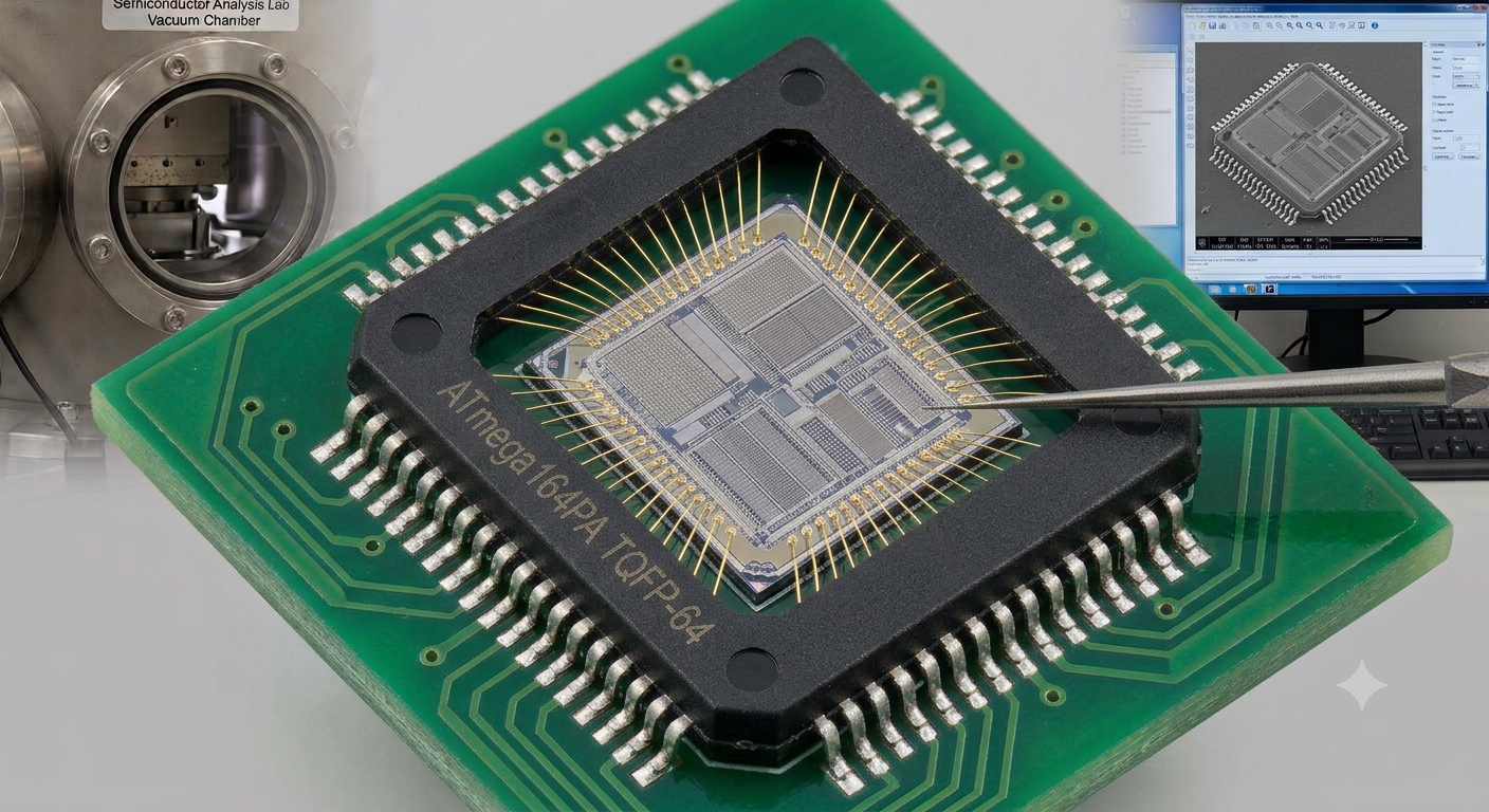
Depending on device condition and project requirements, controlled examination methods may be applied to study internal storage organization and recover available binary and heximal records. Extracted information is organized into usable file and archive formats that support engineering continuity. In selected projects, recovered outputs may assist customers in maintaining product compatibility, validating historical configurations, preparing controlled clone references, or supporting limited duplicate production requirements. Addressing above address 0xA1FF is not recommended, since this will address an external memory location that is already accessed by another (lower) address. To the Application software, the external 32 KB memory will appear as one linear 32 KB address space from 0x2200 to 0xA1FF.
Since the External Memory is mapped after the Internal Memory as shown in Figure 14,only 56KB of External Memory is available by default (address space 0x0000 to 0x21FF is reserved for internal memory). However, it is possible to take advantage of the entire External Memory by masking the higher address bits to zero.
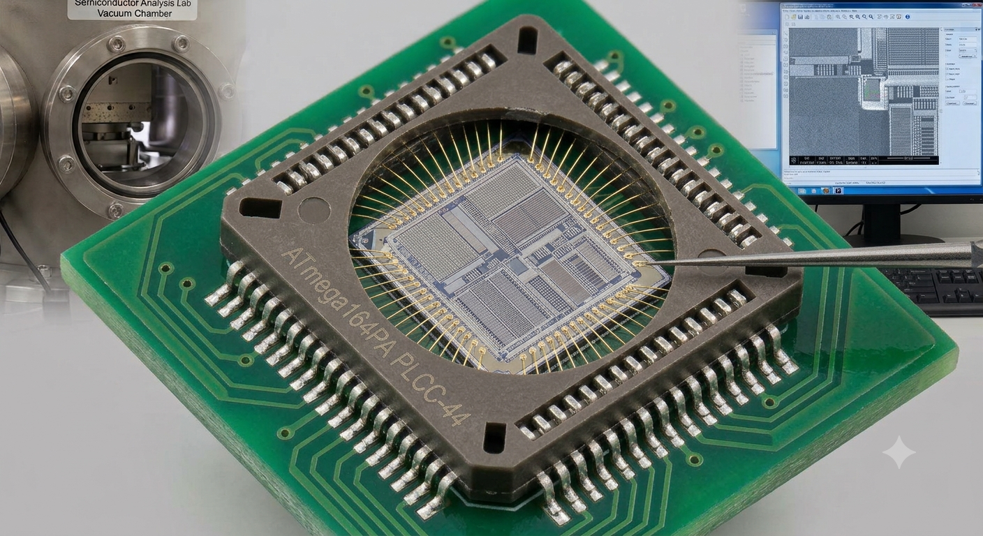
The technical process emphasizes analysis and preservation rather than direct replication. Our workflow focuses on collecting available data, validating integrity, and reconstructing usable engineering assets from available firmware structures. Specialized evaluation techniques may be used to inspect device behavior and support recovery of historical source code references and application program logic. When required and legally authorized, advanced laboratory procedures can assist in understanding storage organization and recovering content from secured or protected environments. Rather than attempting to attack, break, or hack active security systems, the service prioritizes preservation, documentation, and controlled recovery. Where physical inspection is appropriate, carefully managed package analysis and limited decapsulate methods may support interpretation of inaccessible memory regions and help organize recovered binary files into structured engineering outputs.
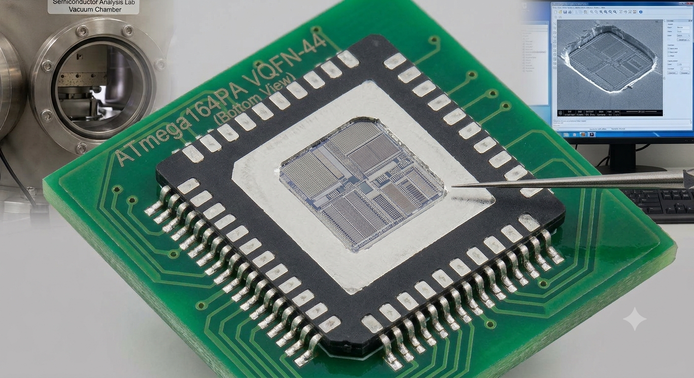
Care must be exercised using this option as most of the memory is masked away. Figure 21 presents the principal clock systems in the AVR and their distribution. All of the clocks need not be active at a given time. In order to reduce power consumption, the clocks to modules not being used can be halted by using different sleep modes, as described in “Power Management and Sleep Modes” on page 51. The clock systems are detailed below.
The CPU clock is routed to parts of the system concerned with operation of the AVR core. Examples of such modules are the General Purpose Register File, the Status Register and the data memory holding the Stack Pointer. Halting the CPU clock inhibits the core from performing general operations and calculations.
The I/O clock is used by the majority of the I/O modules, like Timer/Counters, SPI, and USART. The I/O clock is also used by the External Interrupt module, but note that some external interrupts are detected by asynchronous logic, allowing such interrupts to be detected even if the I/O clock is halted.
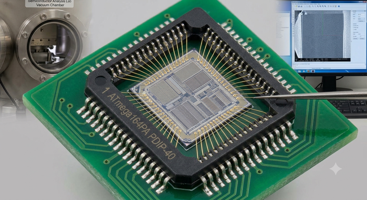
Also note that start condition detection in the USI module is carried out asynchronously when clkI/O is halted, TWI address recognition in all sleep modes.
The Flash clock controls operation of the Flash interface. The Flash clock is usually active simultaneously with the CPU clock. The Asynchronous Timer clock allows the Asynchronous Timer/Counter to be clocked directly from an external clock or an external 32 kHz clock crystal.
For end users, recovering ATmega164PA code creates practical business value across maintenance, modernization, and product lifecycle management. Access to historical firmware, archived data, and reconstructed source code can reduce redevelopment effort, preserve existing hardware investments, and accelerate technical decision making. Organizations can maintain installed equipment, document legacy platforms, and support future upgrades without restarting development from the beginning. By combining embedded expertise with disciplined recovery methodology, our service helps customers preserve critical electronic knowledge and transform inaccessible device content into reusable engineering resources for long-term continuity.
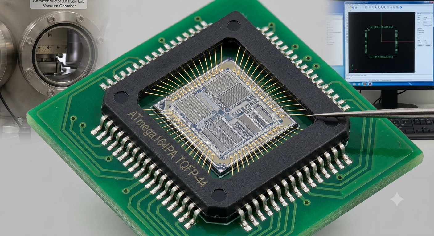
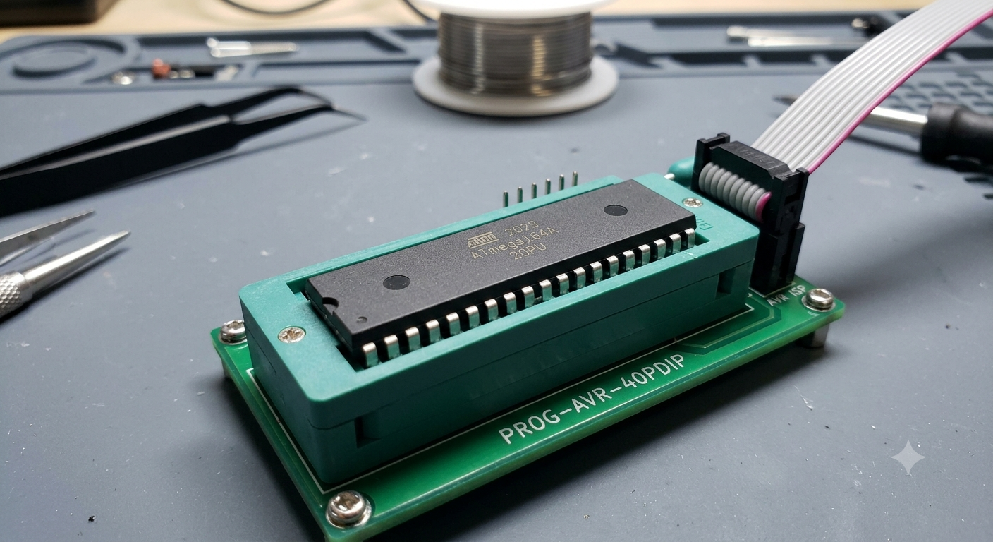
Break Chip ATmega164A Code
The ATmega164A microcontroller is a highly reliable 8-bit AVR RISC-based hardware component widely trusted across industrial robotics, commercial security panels, automotive telemetry interfaces, and medical monitoring devices. What sets this chip apart in demanding engineering landscapes are its unique features, including 16 KB of self-programming flash, a dedicated 512-byte eeprom block, 32 programmable I/O lines, and an integrated 8-channel, 10-bit Analog-to-Digital Converter optimized for highly accurate sensor data ingestion.
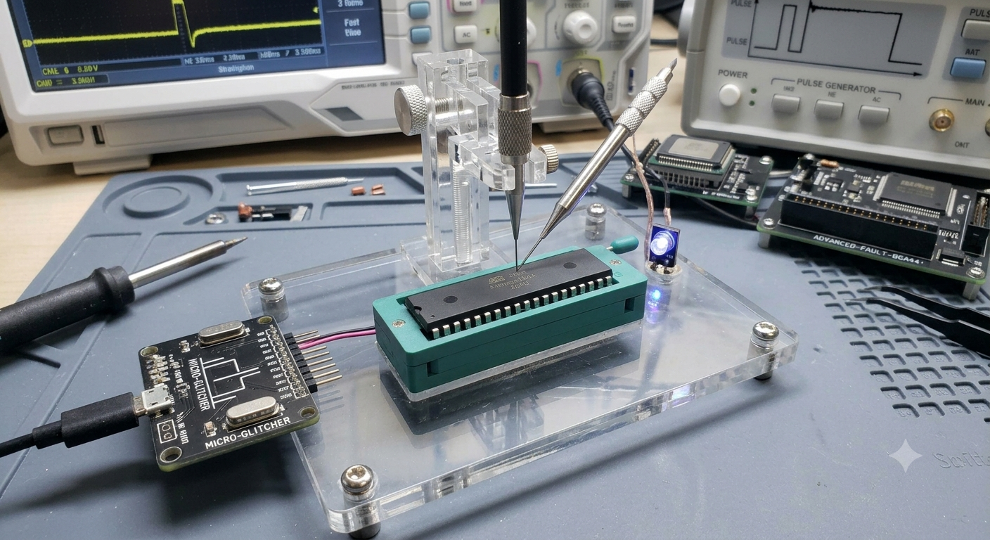
The proprietary instructions that manage these real-time workflows reside safely as an embedded program inside the chip’s memory core. However, manufacturing firms often encounter severe maintenance roadblocks when a vital field system needs to be updated or migrated, but the initial source code, system file, or development archive has vanished. When a supplier shuts down or a specific component faces sudden market obsolescence, finding a reliable hardware extraction route becomes an immediate operational necessity. Our engineering lab offers specialized technical solutions to break chip atmega164a code structures safely, providing an elite path to recovering your invaluable design assets.
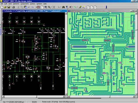
External Memory devices have different timing requirements. To meet these requirements, the XMEM interface provides four different wait-states as shown in Table 5. It is important to consider the timing specification of the External Memory device before selecting the wait-state.
Overriding the high-grade internal security matrix of a locked AVR micro-architecture requires a deep understanding of physical and electrical semiconductor vulnerabilities. To carefully attack, break, and decode the hardware-level readout protections natively built into this secured platform, our engineering facility implements a controlled, multi-phase methodology. First, our laboratory technicians decapsulate the outer protective plastic packaging of the integrated circuit to expose the raw silicon layout and micro-die underneath.
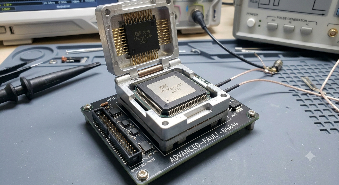
Once the inner microscopic structures are fully visible under high-power microscopy, we deploy specialized fault-injection or precise micro-probing equipment to target the protective code fuses and security bits that natively lock out external programming tools. By temporarily manipulating the internal voltage levels or modifying configuration paths directly on the silicon substrate, our team can safely bypass the chip’s reading restrictions without destroying the underlying hardware. This allows us to smoothly retrieve the tightly guarded firmware, raw data, and application profiles directly out of the hidden flash sectors and internal eeprom memory arrays, translating hidden physical states into a clean, completely uncorrupted heximal file that perfectly mirrors the original machine instructions.
The access time cannot exceed the time from the ALE pulse must be asserted low until data is stable during a read sequence (See tLLRL+ tRLRH – tDVRH in Tables 169 through Tables 176 on pages 376 – 378).
The different wait-states are set up in software. As an additional feature, it is possible to divide the external memory space in two sectors with individual wait-state settings.
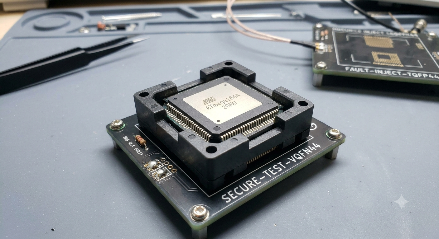
The underlying purpose of choosing to hack, duplicate, or extract software from a protected microcontroller layout is to insulate an enterprise from catastrophic supply chain disruptions and eliminate the astronomical costs of a ground-up system rewrite. When engineering teams lose access to their active program file, our specialized extraction services provide a direct way to salvage vital control logic before a total hardware redesign becomes necessary. Whether your proprietary control code is isolated inside older flash blocks, internal memory arrays, or peripheral PLD matrices, our custom reading tools pull every byte of information safely. Once our team successfully extracts the raw data stream, developers gain the immediate capability to clone the entire logic structure onto a modern, readily available replacement microcontroller. This thorough engineering recovery ensures you can easily duplicate the exact behavioral profiles of your legacy components, establish a fresh software backup, and confidently manufacture drop-in replacement boards, making sure your active production lines keep moving forward without experiencing unexpected field downtime.
Bit 7 – SRE: External SRAM/XMEM Enable
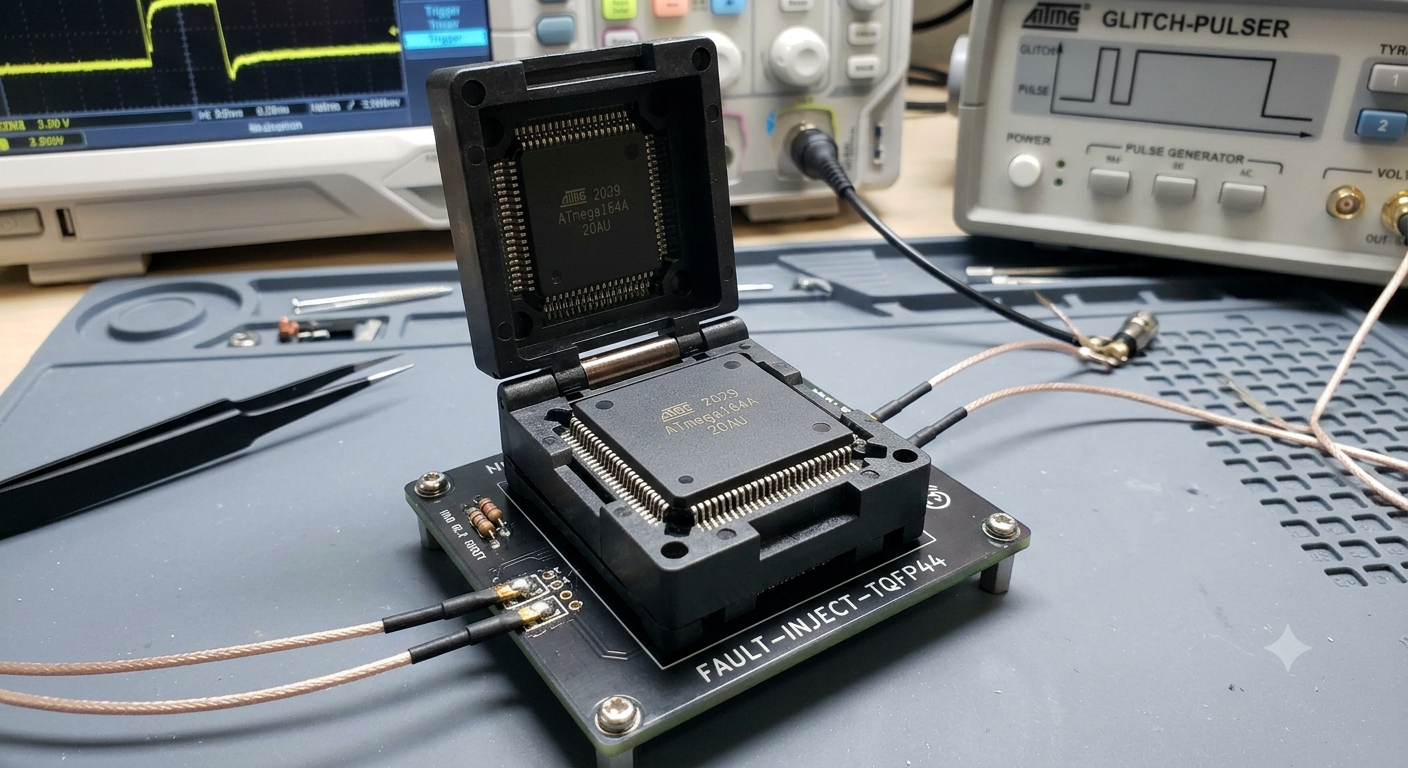
Writing SRE to one enables the External Memory Interface.The pin functions AD7:0, A15:8, ALE, WR, and RD are activated as the alternate pin functions. The SRE bit overrides any pin direction settings in the respective data direction registers. Writing SRE to zero, disables the External Memory Interface and the normal pin and data direction set-tings are used.
Bit 6..4 – SRL2:0: Wait-state Sector Limit
It is possible to configure different wait-states for different External Memory addresses. The external memory address space can be divided in two sectors that have separate wait-state bits. The SRL2, SRL1, and SRL0 bits select the split of the sectors, see Table 4 and Figure 14.
By default, the SRL2, SRL1, and SRL0 bits are set to zero and the entire external memory address space is treated as one sector. When the entire SRAM address space is configured as one sector, the wait-states are configured by the SRW11 and SRW10 bits.
Partnering with an experienced technical team to unlock and recover embedded system software delivers massive financial, operational, and strategic benefits to project managers, maintenance engineers, and hardware developers alike. Instead of dedicating months of expensive R&D time to manually reverse-engineer and re-code a complex encrypted software architecture from scratch—a risky process that notoriously introduces hidden programming bugs—our laboratory provides an efficient pipeline to a fully verified, operational firmware file.
This absolute structural continuity guarantees that every newly generated duplicate circuit board performs identically to the field-proven units your customers already trust. By utilizing our custom microcontroller extraction services, your business effectively mitigates the existential risks of parts obsolescence, safeguards vital corporate intellectual property, and secures a completely predictable, stable roadmap for your industrial hardware investments for many years to come.