Archive for the ‘Recover Chip’ Category
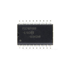
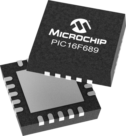
 Recover Chip PIC16F689 Flash
When a device depends on a Microchip PIC16F689 for control, timing, or sensor interfacing, losing access to the on-chip flash or EEPROM can halt production, disrupt service, or erase critical calibration data. Our service, searchable under the keyword Recover Chip PIC16F689 Flash, helps legitimate owners and authorized technicians open, readout, restore, and duplicate the firmware/binary/heximal contents of this microcontroller while maintaining strict legal, ethical, and confidentiality standards. We emphasize recovery and preservation — not publishing methods to crack or illegally hack protections.
The PIC16F689 is commonly embedded in devices where small, reliable control programs and configuration archives are essential. Clients come to us to restore corrupted program files, copy firmware for authorized spares provisioning, clone configuration data for scaled deployment, or duplicate critical archives before servicing legacy systems. In many scenarios the firmware or memory image is protected, locked, or encrypted by design, so an authorized recovery partner is required to retrieve usable program files without risking further damage.
We can Recover Chip PIC16F689 Flash, please view the CHIP PIC16F689 features below for your reference:
High-Performance RISC CPU:
· Only 35 Instructions to Learn:
– All single-cycle instructions except branches
· Operating Speed:
– DC – 20 MHz oscillator/clock input
– DC – 200 ns instruction cycle
· Interrupt Capability
· 8-level Deep Hardware Stack
Low-Power Features:
The PIC16F689’s blend of I/O, timers, and analog features makes it popular across many industries:
- Consumer electronics and appliance controllers.
- Industrial monitoring and simple automation modules.
- Instrumentation such as small data loggers and measurement front-ends.
- Aftermarket automotive or specialty embedded projects that rely on compact, efficient code.
In these contexts, recovered binary or heximal files enable quicker repairs, validated backups, and smoother migration to replacement hardware.
· Standby Current:
– 50 nA @ 2.0V, typical
· Operating Current:
– 11 ìA @ 32 kHz, 2.0V, typical
– 220 ìA @ 4 MHz, 2.0V, typical
· Watchdog Timer Current:
– 1 ìA @ 2.0V, typical
· Direct, Indirect and Relative Addressing modes
Peripheral Features:
Special Microcontroller Features:
· Precision Internal Oscillator:
– Factory calibrated to ±1%
– Software selectable frequency range of 8 MHz to 125 kHz
– Software tunable
– Two-Speed Start-Up mode
– Crystal fail detect for critical applications
– Clock mode switching during operation for power savings
· Power-Saving Sleep mode
· Wide Operating Voltage Range (2.0V-5.5V)
· Industrial and Extended Temperature Range
· Power-on Reset (POR)
· Power-up Timer (PWRT) and Oscillator Start-up Timer (OST)
· Brown-out Reset (BOR) with Software Control Option
· Enhanced Low-Current Watchdog Timer (WDT) with on-chip oscillator (software selectable nominal 268 seconds with full prescaler) with software enable
· Multiplexed Master Clear with Weak Pull-up or Input Only Pin
· Programmable Code Protection
· High-Endurance Flash/EEPROM Cell:
– 100,000 write Flash endurance
– 1,000,000 write EEPROM endurance
– Flash/Data EEPROM retention: > 40 years
· 12 I/O Pins with Individual Direction Control:
– High-current source/sink for direct LED drive
– Interrupt-on-change pin
– Individually programmable weak pull-ups
– Ultra Low-Power Wake-up
· Analog Comparator module with:
– Two analog comparators
– Programmable On-chip Voltage Reference (CVREF) module (% of VDD)
– Comparator inputs and outputs externally accessible
· A/D Converter:
– 10-bit resolution and 8 channels
· Timer0: 8-bit Timer/Counter with 8-bit Programmable Prescaler
· Enhanced Timer1:
– 16-bit timer/counter with prescaler
– External Timer1 Gate (count enable)
– Option to use OSC1 and OSC2 in LP mode as Timer1 oscillator if INTOSC mode selected
· Enhanced USART Module:
– Supports RS-485, RS-232, LIN 2.0/2.1 and J2602
– Auto-Baud Detect
– Auto-wake-up on Start bit
· In-Circuit Serial Programming™ (ICSP™) via two pins
The PIC16F689 integrates program flash, EEPROM, and mixed-signal peripherals in a compact package. Its memory layout and on-chip configuration bits influence how the source code (if available) maps to raw files and how sensitive calibration data is stored. Because many designs apply protective settings to prevent unauthorized copying, recovery must be planned carefully to avoid corrupting valuable data.
What we provide (high level & non-actionable)
Our engagements are oriented around ethical recovery. Services include: validated extraction of on-chip images producing heximal or binary dumps (where lawful), integrity checks and documented verification, and high-level disassembly summaries to help engineers interpret the recovered program. We can assist with restoring devices to operation using recovered images and preparing migration packages for replacement boards. We do not provide step-by-step instructions to crack, decrypt, or bypass manufacturer protections — all work is performed only with proof of ownership or explicit authorization.
Conceptual workflow and purpose
A responsible recovery effort begins with authorization and a risk assessment. Non-destructive techniques are used to obtain a reliable memory archive, which is then validated and annotated. The primary purpose is practical: reduce downtime, secure backups, enable authorized copying or cloning, and preserve investment in specialized hardware.
Benefits and limitations
Clients gain rapid restoration of functionality, secure copies of previously inaccessible firmware and configuration archives, and the ability to duplicate systems for authorized maintenance. Limitations can include partial corruption, proprietary integrity checks, or layered locked settings — outcomes that may restrict full source-level recovery. We make feasibility and likely results clear before work begins.
Legal & ethical safeguards
Every project requires ownership verification and a confidentiality agreement. Our mission is to unlock and recover embedded software for lawful, constructive purposes only — repair, continuity, authorized audit, and migration.
If you need to Recover Chip PIC16F689 Flash for legitimate recovery or maintenance, our experienced team provides confidential, professional support to retrieve and document embedded firmware while protecting your IP and operational continuity.
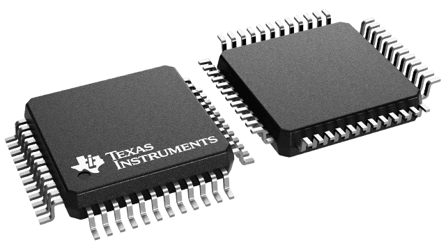
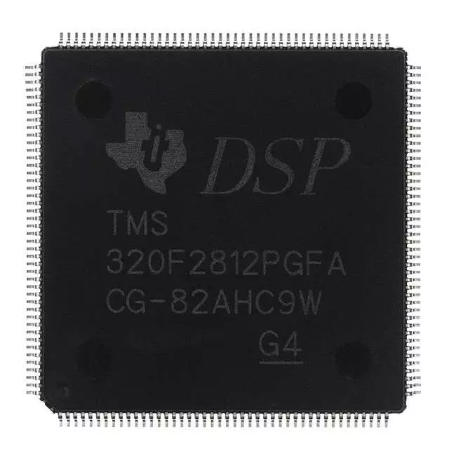
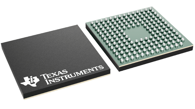
Recover Microcontroller TMS320F2812PGFA Firmware
The Texas Instruments TMS320F2812PGFA is a powerful digital signal processor (DSP) microcontroller widely used in high-performance industrial and automotive applications. Its ability to handle complex real-time control systems makes it a cornerstone in embedded designs such as motor drives, robotics, power conversion, and automotive electronics. However, with its advanced functionality comes sophisticated security mechanisms, designed to keep its firmware protected from unauthorized access. When the original source code, binary, or heximal file becomes inaccessible due to locked or encrypted flash memory, the need arises to recover microcontroller TMS320F2812PGFA firmware for further analysis, modification, or duplication.
Why Recovery Services Are Needed
There are countless situations where engineers or end users may need to restore or recover the firmware from this secured device. The original program file may be lost, corrupted, or stored in obsolete archives. In other cases, businesses may need to copy or clone the firmware from one protected chip to another for repair, testing, or mass duplication. The protective fuse bits of the TMS320F2812PGFA, once enabled, restrict normal access to the memory, making conventional readout tools ineffective. This creates a need for specialized techniques to unlock or open the device.
Unique Features of the TMS320F2812PGFA
This microcontroller offers unique advantages that make it a preferred choice across industries:
- High-Performance DSP Core: Capable of handling advanced algorithms in real-time.
- Extensive On-Chip Memory: Integrated flash and RAM for storing data, firmware, and critical program files.
- Peripheral Integration: Includes ADCs, communication interfaces, and PWM modules for motor and control systems.
- Security Features: Locking mechanisms and encryption options designed to protect sensitive firmware.
Because of these features, recovering firmware from this chip requires not just basic tools, but deep technical expertise in bypassing secured mechanisms without damaging the device.
General Steps in Breaking Protection
Although exact methods vary depending on chip configuration, the general process for cracking or decoding protected microcontrollers like the TMS320F2812PGFA involves several stages:
- Device Analysis – Identifying the locked memory regions, security fuse states, and encryption measures applied.
- Physical or Logical Access – Applying precision tools to interface with memory and bypass protective barriers.
- Disabling Fuse Bit Protection – Specialized methods are used to neutralize fuse-bit restrictions without corrupting stored data.
- Firmware Extraction – Once unlocked, the heximal firmware is read out from flash, EEPROM, or other memory banks.
- Conversion & Reconstruction – The extracted binary or data file is decoded into a usable format, sometimes decompiled into C/C++ source code for easier analysis.
- Verification & Duplication – The recovered firmware is validated and can be duplicated, copied, or cloned onto new devices as required.
Applications Across Industries
The TMS320F2812PGFA is commonly embedded in:
- Industrial Automation Systems – Robotics, motor drives, and process controllers.
- Automotive Electronics – Engine management, braking, and safety systems.
- Power Systems – Renewable energy inverters, UPS units, and high-efficiency converters.
- Aerospace and Defense – Rugged control systems requiring reliable real-time DSP performance.
In each of these fields, losing access to the embedded firmware could mean costly downtime or inability to restore critical equipment. That is why professional services to recover microcontroller TMS320F2812PGFA firmware are invaluable.
We can Recover Microcontroller TMS320F2812PGFA Firmware, please view below the Microcontroller TMS320F2812PGFA features for your reference:
High-Performance Static CMOS Technology
– 150 MHz (6.67-ns Cycle Time)
– Low-Power (1.8-V Core at 135 MHz, 1.9-V Core at 150 MHz, 3.3-V I/O) Design
· JTAG Boundary Scan Support (1)
· High-Performance 32-Bit CPU ( TMS320C28x™)
– 16 x 16 and 32 x 32 MAC Operations
– 16 x 16 Dual MAC
– Harvard Bus Architecture
– Atomic Operations
– Fast Interrupt Response and Processing
– Unified Memory Programming Model
– 4M Linear Program/Data Address Reach
– Code-Efficient (in C/C++ and Assembly)
– TMS320F24x/LF240x Processor Source Code Compatible to Copy microcontroller
· On-Chip Memory
– Flash Devices: Up to 128K x 16 Flash (Four 8K x 16 and Six 16K x 16 Sectors)
– ROM Devices: Up to 128K x 16 ROM
– 1K x 16 OTP ROM
– L0 and L1: 2 Blocks of 4K x 16 Each Single-Access RAM (SARAM)
– H0: 1 Block of 8K x 16 SARAM
– M0 and M1: 2 Blocks of 1K x 16 Each SARAM
· Boot ROM (4K x 16)
– With Software Boot Modes
– Standard Math Tables
· External Interface (2812)
– Over 1M x 16 Total Memory
– Programmable Wait States
– Programmable Read/Write Strobe Timing
– Three Individual Chip Selects
· Endianness: Little Endian
· Clock and System Control
– Dynamic PLL Ratio Changes Supported
– On-Chip Oscillator
– Watchdog Timer Module
· Three External Interrupts
· Peripheral Interrupt Expansion (PIE) Block That Supports 45 Peripheral Interrupts
· Three 32-Bit CPU-Timers
· 128-Bit Security Key/Lock
– Protects Flash/ROM/OTP and L0/L1 SARAM
– Prevents Firmware Reverse-Engineering
· Motor Control Peripherals
– Two Event Managers (EVA, EVB)
– Compatible to 240xA Devices
· Serial Port Peripherals
– Serial Peripheral Interface (SPI)
– Two Serial Communications Interfaces (SCIs), Standard UART
– Enhanced Controller Area Network (eCAN)
– Multichannel Buffered Serial Port (McBSP)
· 12-Bit ADC, 16 Channels
– 2 x 8 Channel Input Multiplexer
– Two Sample-and-Hold
– Single/Simultaneous Conversions
– Fast Conversion Rate: 80 ns/12.5 MSPS
· Up to 56 General-Purpose I/O (GPIO) Pins
· Advanced Emulation Features
– Analysis and Breakpoint Functions
– Real-Time Debug via Hardware
· Development Tools Include
– ANSI C/C++ Compiler/Assembler/Linker
– Code Composer Studio™ IDE
– DSP/BIOS™
– JTAG Scan Controllers(1)
· Low-Power Modes and Power Savings
– IDLE, STANDBY, HALT Modes Supported
– Disable Individual Peripheral Clocks
Recovering protected or encrypted firmware from the TMS320F2812PGFA requires advanced expertise, precise methods, and an understanding of both hardware and software security. By applying proven techniques to crack locked memory, decode binary data, and unlock encrypted program files, it becomes possible to restore the original firmware and duplicate it for practical applications. This ensures that valuable embedded systems continue to operate efficiently, while also allowing engineers to analyze and improve upon existing designs.
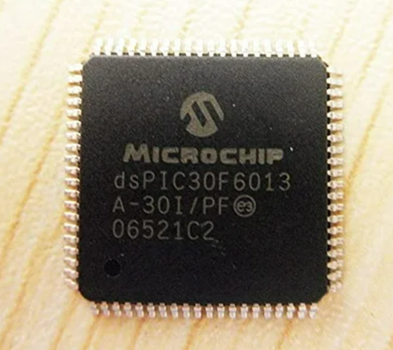
Recover MCU dsPIC30F6013A30IP Firmware
The Microchip dsPIC30F6013A is a powerful 16-bit Digital Signal Controller (DSC) widely adopted in industrial automation, automotive systems, medical devices, and high-performance embedded applications. Its combination of digital signal processing with traditional microcontroller capabilities makes it a popular choice for engineers who require real-time control and reliability. However, the very features that make this chip valuable—such as its protective lock bits, secured program memory, and encrypted data storage—also create challenges when users need to access or recover MCU dsPIC30F6013A firmware.
Why Firmware Recovery Matters
Firmware serves as the heart of any embedded design. The binary or heximal files stored in the flash, EEPROM, and other memory regions control every operation of the system. When this firmware becomes corrupted, locked, or otherwise inaccessible, the entire device may be unusable. Being able to restore, copy, or duplicate the original program file is essential for maintenance, legacy support, or further development.
In many cases, manufacturers activate fuse bits to prevent outsiders from reading the firmware. While these security measures help protect intellectual property, they can also create difficulties for end users who legitimately need access to their own firmware. Our specialized service focuses on overcoming these barriers and providing a reliable path to recover the required data.
General Steps to Unlock Protected Firmware
Recovering dsPIC30F6013A firmware often involves several stages:
- Initial Device Analysis – Inspecting the target chip, identifying the security status, and verifying the condition of the flash and EEPROM.
- Bypassing Protection – Techniques to disable fuse bits or bypass secured configurations, allowing access to the locked memory.
- Data Extraction – Reading out the binary or heximal archive from the program memory and EEPROM.
- Disassembly and Conversion – When needed, decoding or decompiling the binary file into more understandable forms such as assembly or partial source code.
- Validation and Restoration – Ensuring that the recovered file is accurate, functional, and ready for reprogramming into new devices or used for analysis.
These steps may require advanced tools and a combination of hardware probing, cryptographic decode/decrypt methods, and firmware hacking strategies.
Applications of dsPIC30F6013A
The dsPIC30F6013A is widely used in:
- Automotive systems – engine control, sensor interfaces, and powertrain modules.
- Industrial automation – motor control, real-time monitoring, and robotics.
- Medical equipment – secured embedded devices for patient monitoring and diagnostics.
- Consumer electronics – high-efficiency devices where digital signal processing is critical.
In each case, the ability to unlock, open, or recover the firmware ensures product longevity, supports upgrades, and enables manufacturers or end users to duplicate or redevelop systems without losing functionality.
We can Recover MCU dsPIC30F6013A30IP Firmware, please view below MCU DSPIC30F6013A30IP features for your reference:
The dsPIC30F family of DSCs contains a region of on-chip memory used to simplify device programming. This region of memory can store a programming executive, which allows the dsPIC30F to be programmed faster than the traditional means. Once the programming executive is stored to memory by an external programmer (such as Microchip’s MPLAB ICD 2, MPLAB PM3, PRO MATE® II, or MPLAB REAL uses control codes to serially execute instructions on the dsPIC30F device.
This specification describes the ICSP and Enhanced ICSP programming methods. Section 3.0 “Programming Executive Application” describes the programming executive application and Section 5.0 “Device Programming” describes its application programmer’s interface for the host programmer before Recover MCU. Section 11.0 “ICSP™ Mode” describes the ICSP programming method. ICE™), it can then interact with the external programmer to efficiently program devices.
2.1 Hardware Requirements
The programmer and programming executive have a master-slave relationship, where the programmer is the master programming device and the programming executive is the slave.
Circuit Engineering Company Limited continues to be recognized as the Southern China Leader in Services for IC Break, MCU attack, MCU Recover, Microcontroller Copy service. With the advancement of today’s modern circuit board technology, it is more important than ever to have specialists available to help you at a moment’s notice. Our engineering and commercial teams collectively have a vast amount of electronic experience covering field include Consumer Electronics, Industrial Automation Electronics, Wireless Communication Electronics., etc. For more information please contact us through email.
Recovering MCU dsPIC30F6013A firmware is a complex process that requires expertise in reverse engineering, cryptographic bypass, and secure memory handling. By extracting and restoring the protected program and data files from this versatile microcontroller, it becomes possible to extend the life of valuable embedded systems, replicate critical functions, or simply safeguard against data loss. For industries relying on the dsPIC30F6013A, having the ability to recover its firmware can be the key to maintaining competitiveness and ensuring continued operation of vital equipment.
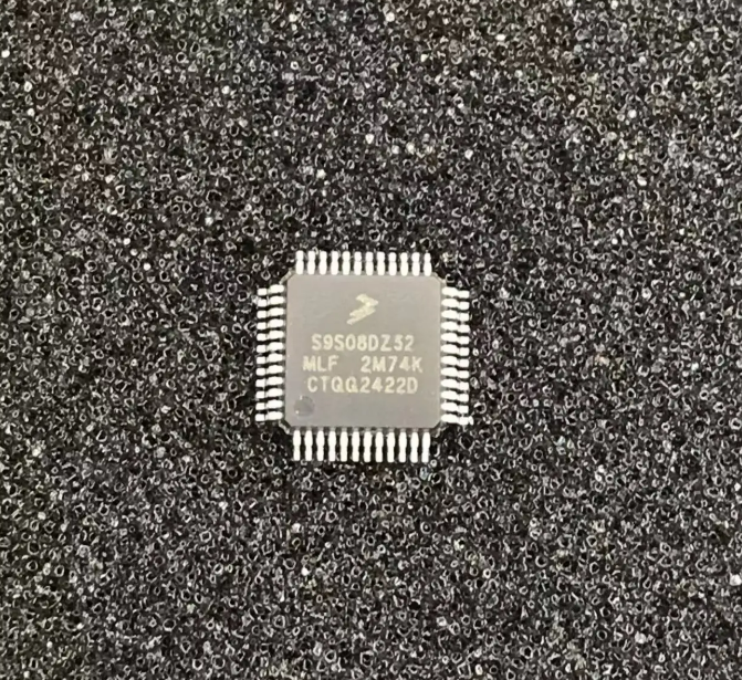
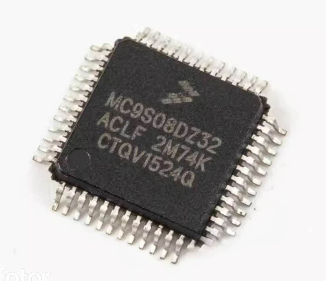
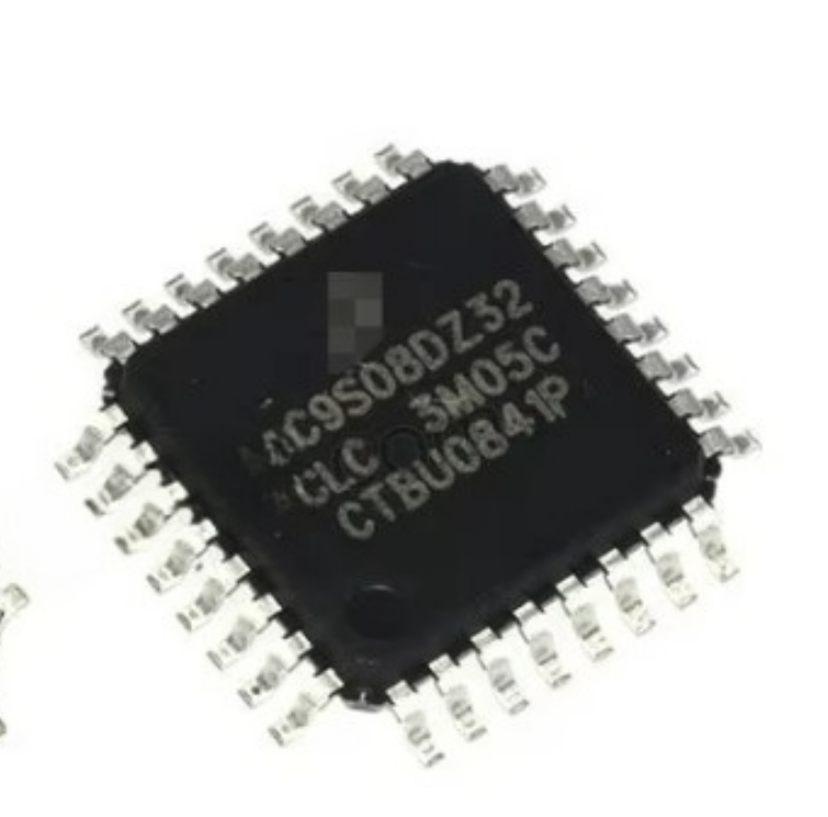
Recover Chip MC9S08DZ32ACLC Firmware
The MC9S08DZ32ACLC microcontroller, developed by Freescale (now NXP), is widely used in automotive, industrial, and consumer electronics applications. Its popularity stems from its reliable performance, low power consumption, and robust integration of flash memory, EEPROM, and peripheral features. However, recovering firmware from this protected and embedded chip poses significant challenges due to its security mechanisms. At Circuit Engineering Co., Ltd, we offer professional and precise services to recover Chip MC9S08DZ32ACLC firmware, enabling access to valuable system-level data and binary files for legitimate engineering and recovery purposes.
Why Recover MC9S08DZ32ACLC Firmware?
This chip is commonly deployed in automotive control modules, dashboards, sensors, and smart motor applications. Engineers, OEMs, and repair technicians often face situations where the original firmware is lost, corrupted, or no longer accessible due to locked or encrypted flash memory. In such cases, recreating the product, cloning behavior, or simply restoring the embedded function becomes impossible without access to the original firmware. That’s where our service becomes essential.
Our Advanced Firmware Recovery Process
We utilize a combination of hardware probing, software cracking, and firmware decoding techniques to unlock, decrypt, and extract the firmware from the flash and EEPROM memory inside the MC9S08DZ32ACLC. Our expertise allows us to crack secured chips and duplicate the binary/heximal files while maintaining data integrity and completeness.
Once access is established, we copy and clone the program data, restoring it into a readable hex file or reconstructing it into assembly or source code formats as needed. This allows our clients to not only recover the program but also analyze, test, or modify it for updated product development, security audits, or system migration.
Key Services We Provide:
- Recover Chip MC9S08DZ32ACLC Firmware from locked or secured systems
- Clone and duplicate the embedded flash contents into new units
- Restore lost firmware files, EEPROM data, or archived program structures
- Decode and decrypt binary firmware for analysis or reuse
- Unlock encrypted program memory for reverse engineering or debugging
- Provide reconstructed heximal or binary files for reprogramming or documentation
Unique Features of the MC9S08DZ32ACLC
This 8-bit MCU from Freescale features:
- Up to 32KB of flash memory and 2KB EEPROM
- Internal clock generators and multiple communication interfaces (CAN, SCI, SPI, I²C)
- Enhanced control and diagnostics support for automotive-grade environments
- Advanced interrupt handling and low EMI design, making it ideal for mission-critical applications
Its robust security options—including memory protection schemes—make firmware access nearly impossible without specialized equipment and technical insight. That’s why your choice of service provider is critical.
Trusted, Confidential, and Accurate
All projects handled by our engineering team are executed with strict confidentiality and technical accuracy. Whether you’re looking to restore a malfunctioning device, duplicate firmware for production, or analyze a secured program archive, we deliver results efficiently and securely.
We can Recover Chip MC9S08DZ32ACLC Firmware, please view below the Chip MC9S08DZ32ACLC features for your reference:
8-Bit HCS08 Central Processor Unit (CPU)
· 40-MHz HCS08 CPU (20-MHz bus)
· HC08 instruction set with added BGND instruction
· Support for up to 32 interrupt/reset sources
On-Chip Memory
· Flash read/program/erase over full operating voltage and temperature
— MC9S08DZ60 = 60K
— MC9S08DZ48 = 48K
— MC9S08DZ32 = 32K
— MC9S08DZ16 = 16K
· Up to 2K EEPROM in-circuit programmable memory;
8-byte single-page or 4-byte dual-page erase sector;
Program and Erase while executing Flash; Erase abort
· Up to 4K random-access memory (RAM)
Power-Saving Modes
· Two very low power stop modes
· Reduced power wait mode
· Very low power real time interrupt for use in run, wait, and stop Clock Source Options
· Oscillator (XOSC) — Loop-control Pierce oscillator;
Crystal or ceramic resonator range of 31.25 kHz to 38.4 kHz or 1 MHz to 16 MHz
· Multi-purpose Clock Generator (MCG) — PLL and FLL modes (FLL capable of 1.5% deviation using internal temperature compensation); Internal reference clock with trim adjustment (trimmed at factory, with trim value stored in flash); External reference with oscillator/resonator options in the process of Copy microcontroller
System Protection
· Watchdog computer operating properly (COP) reset with option to run from backup dedicated 1-kHz internal clock source or bus clock
· Low-voltage detection with reset or interrupt; selectable trip points
· Illegal opcode detection with reset
· Illegal address detection with reset
· Flash block protect
· Loss-of-lock protection
Peripherals
· ADC — 24-channel, 12-bit resolution, 2.5 ìs conversion time, automatic compare function, temperature sensor, internal bandgap reference channel
· ACMPx — Two analog comparators with selectable interrupt on rising, falling, or either edge of comparator output; compare option to fixed internal bandgap reference voltage.
· MSCAN — CAN protocol – Version 2.0 A, B; standard and extended data frames; Support for remote frames; Five receive buffers with FIFO storage scheme; Flexible identifier acceptance filters programmable as: 2 x 32-bit, 4 x 16-bit, or 8 x 8-bit
· SCIx — Two SCIs supporting LIN 2.0 Protocol and SAE J2602 protocols; Full duplex non-return to zero (NRZ); Master extended break generation; Slave extended break detection; Wakeup on active edge.
· SPI — Full-duplex or single-wire bidirectional; Double-buffered transmit and receive; Master or Slave mode; MSB-first or LSB-first shifting
· IIC — Up to 100 kbps with maximum bus loading; Multi-master operation; Programmable slave address; General Call Address; Interrupt driven byte-by-byte data transfer
· TPMx — One 6-channel (TPM1) and one 2-channel (TPM2); Selectable input capture, output compare, or buffered edge-aligned PWM on each channel.
· RTC — (Real-time counter) 8-bit modulus counter with binary or decimal based prescaler; Real-time clock capabilities using external crystal and RTC for precise time base, time-of-day, calendar or task scheduling functions; Free running on-chip low power oscillator (1 kHz) for cyclic wake-up without external components Input/Output
· 53 general-purpose input/output (I/O) pins and 1 input-only pin
· 24 interrupt pins with selectable polarity on each pin.
· Hysteresis and configurable pull device on all input pins.
· Configurable slew rate and drive strength on all output pins.
Package Options
· 64-pin low-profile quad flat-pack (LQFP) — 10×10 mm
· 48-pin low-profile quad flat-pack (LQFP) — 7×7 mm
· 32-pin low-profile quad flat-pack (LQFP) — 7×7 mm
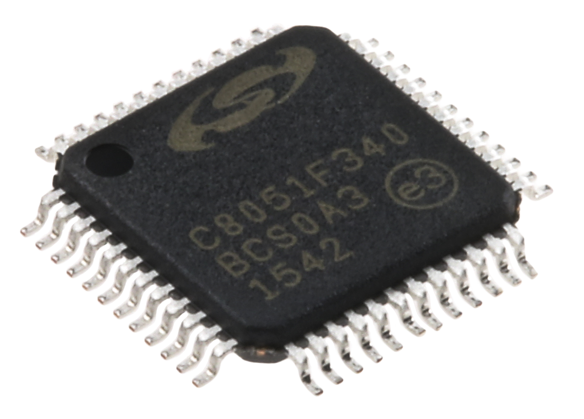
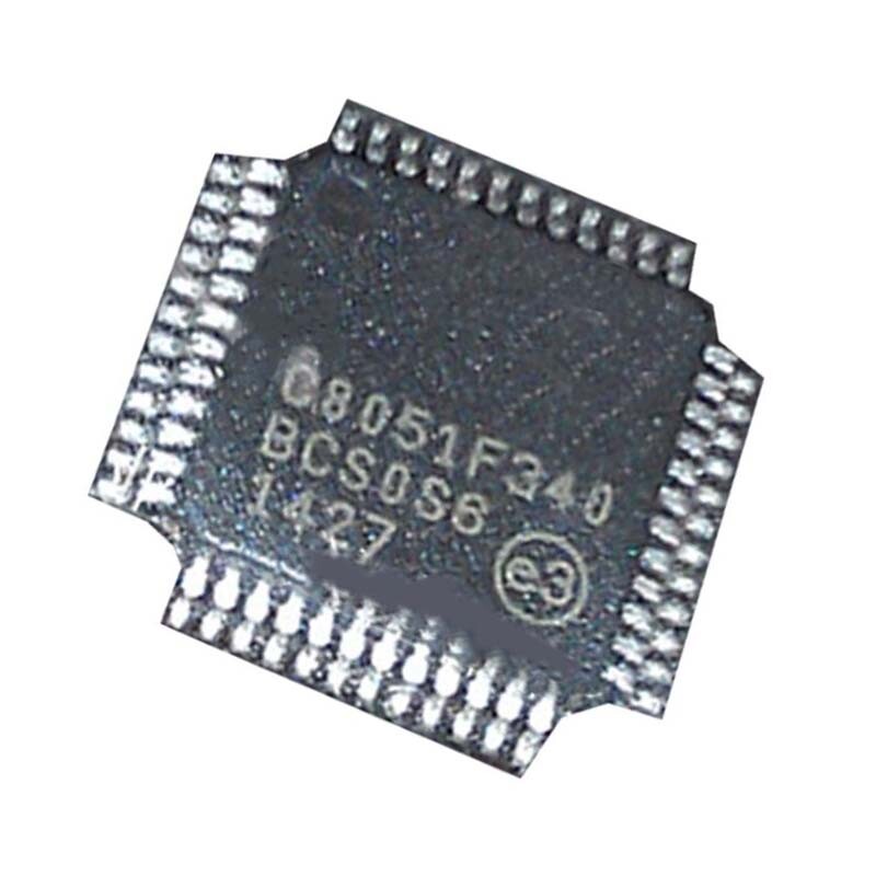
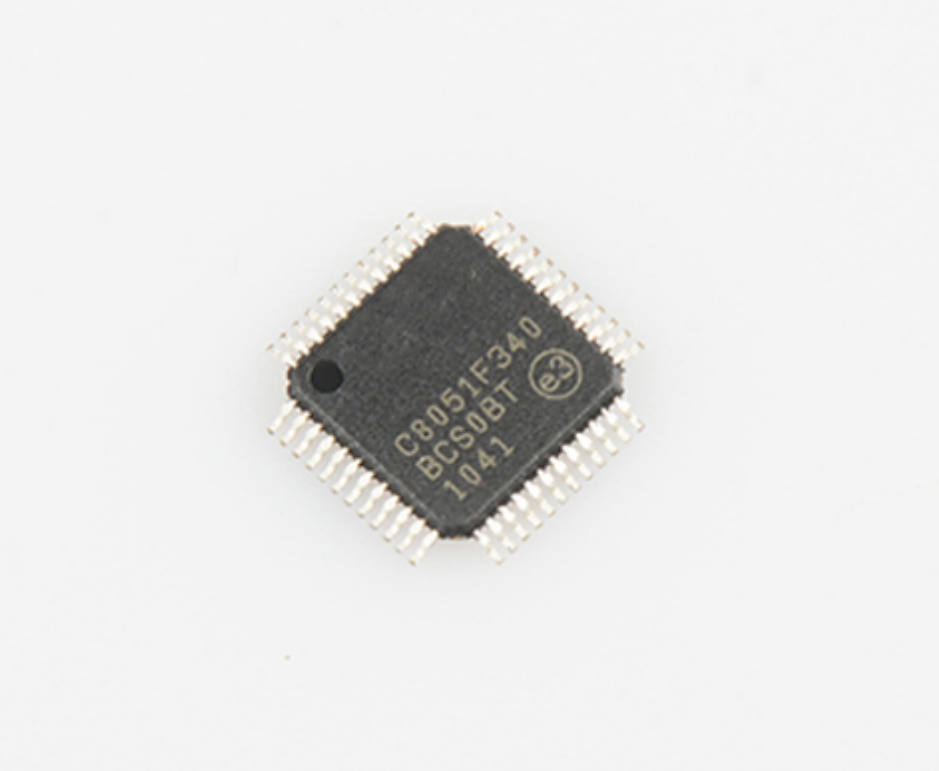
Recover Chip C8051F340 Firmware
The Silicon Labs C8051F340 is a powerful embedded microcontroller widely used in industrial control systems, USB devices, instrumentation, and other high-performance applications. With integrated USB 2.0 functionality, high-speed 8051 core, and multiple I/O peripherals, it offers a compact yet feature-rich solution for developers. However, when the firmware, heximal file, or internal flash memory becomes corrupted, lost, or inaccessible due to security locking mechanisms, it presents a significant challenge for developers, maintainers, or forensic analysts.
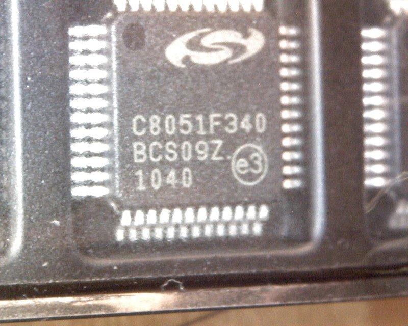
At CIRCUIT ENGINEERING CO., LTD, we provide expert services to recover chip C8051F340 firmware from secured or protected devices—whether the data has been encrypted, locked, or subjected to proprietary code protection features. Our advanced techniques allow us to restore, crack, unlock, and even clone the essential program files, memory contents, or binary archives stored inside the flash or EEPROM of the MCU.
Recover Chip C8051F340 Firmware include the program from flash and data from eeprom memory through MCU Cracking technique, then replicate the content to other blank Microcontroller C8051F340;
The C8051F340 integrates code security features that prevent easy access to the internal firmware, especially through standard debugging or programming tools. Once the read protection is enabled, developers are typically locked out from reading or duplicating the original source code, even when they are the rightful owners of the system.
Using a combination of hardware-assisted attack methods, low-level protocol analysis, and carefully designed reverse engineering routines, our engineers can decode, decrypt, and copy the secured firmware binary or heximal file from the microcontroller. We handle devices in a non-destructive manner whenever possible, ensuring the integrity of the hardware while extracting the vital program data or code archive.
Many end users or manufacturers come to us for one of several reasons:
- Legacy system support where original firmware has been lost or corrupted
- Board-level repairs requiring firmware duplication or restoration
- Security audits of existing systems for vulnerability assessment
- IP preservation, especially when developers or contractors are no longer available
Losing the firmware file for a secured chip like the C8051F340 can bring an entire production line or critical application to a halt. Our firmware recovery service ensures that your valuable intellectual property is not permanently lost.
Analog Peripherals
High Speed 8051 µC Core 10-Bit ADC (C8051F340/1/2/3/4/5/6/7/A/B only)
Pipelined instruction architecture; executes 70% of Up to 200 ksps
Built-in analog multiplexer with single-ended and differential mode
VREF from external pin, internal reference, or VDD
Instructions in 1 or 2 system clocks 48 MIPS and 25 MIPS versions available.
Expanded interrupt handler
· Built-in temperature sensor
· External conversion start input option
Two comparators Internal voltage reference
Memory
– 4352 or 2304 Bytes RAM
– 64 or 32 kB Flash; In-system programmable in 512-byte
(C8051F340/1/2/3/4/5/6/7/A/B only)
– Brown-out detector and POR Circuitry
USB Function Controller
– USB specification 2.0 compliant
– Full speed (12 Mbps) or low speed (1.5 Mbps) operation sectors
Digital Peripherals
– 40/25 Port I/O; All 5 V tolerant with high sink current
– Hardware enhanced SPI™, SMBus™, and one or two enhanced UART serial ports
Integrated clock recovery; no external crystal required for full speed or low speed
Supports eight flexible endpoints 1 kB USB buffer memory
Four general purpose 16-bit counter/timers
16-bit programmable counter array (PCA) with five capture/compare modules
External Memory Interface (EMIF)
Integrated transceiver; no external resistors required
Clock Sources
On-Chip Debug
Internal Oscillator: ±0.25% accuracy with clock recovery
On-chip debug circuitry facilitates full speed, non-intruenabled. Supports all USB and UART modes sive in-system debug (No emulator required) Provides breakpoints, single stepping, inspect/modify memory and registers
External Oscillator: Crystal, RC, C, or clock (1 or 2 Pin modes)
Low Frequency (80 kHz) Internal Oscillator Superior performance to emulation systems using ICE-chips, target pods, and sockets
Voltage Supply Input: 2.7 to 5.25 V
– Voltages from 3.6 to 5.25 V supported using On-Chip Voltage Regulator
– Can switch between clock sources on-the-fly
Packages
– 48-pin TQFP (C8051F340/1/4/5/8/C)
– 32-pin LQFP (C8051F342/3/6/7/9/A/B/D)
– 5×5 mm 32-pin QFN (C8051F342/3/6/7/9/A/B)
Temperature Range: –40 to +85 °C
We offer a full-service solution: from physical chip access to disassembly, heximal decoding, and even C-source reconstruction. Whether your C8051F340 has been locked, encrypted, or is simply part of a secured legacy embedded system, we are equipped to open, copy, and replicate its full functionality.
Reach out to Circuit Engineering Co., LTD today and let us help you recover chip C8051F340 firmware — securely, professionally, and with precision.
Recover Microcontroller STM32F103RET6TR Code
Recover Microcontroller STM32F103RET6TR Code from its memory which include the flash and eeprom, then copy the program to blank MCU STM32F103RET6 after MCU Cracking;
Recover Microcontroller STM32F103RET6TR Code from its memory which include the flash and eeprom, then copy the program to blank MCU STM32F103RET6 after MCU Cracking;
Features
ARM 32-bit Cortex™-M3 CPU Core
– 72 MHz maximum frequency, 1.25 DMIPS/MHz (Dhrystone 2.1) performance at 0 wait state memory access
– Single-cycle multiplication and hardware division
Memories
– 16 or 32 Kbytes of Flash memory
VFQFPN48 (7 × 7 mm)
VFQFPN36 (6 × 6 mm)
– 6 or 10 Kbytes of SRAM Clock, reset and supply management
– 2.0 to 3.6 V application supply and I/Os
– POR, PDR, and programmable voltage detector (PVD)
– 4-to-16 MHz crystal oscillator
– Internal 8 MHz factory-trimmed RC
– Internal 40 kHz RC
– PLL for CPU clock
– 32 kHz oscillator for RTC with calibration Low power
– Sleep, Stop and Standby modes
– VBAT supply for RTC and backup registers 2 x 12-bit, 1 µs A/D converters (up to 16 channels)
– Conversion range: 0 to 3.6 V
– Dual-sample and hold capability
– Temperature sensor DMA
– 7-channel DMA controller Debug mode
– Serial wire debug (SWD) & JTAG interfaces 6 timers
– Two 16-bit timers, each with up to 4 IC/OC/PWM or pulse counter and quadrature (incremental) encoder input
– 16-bit, motor control PWM timer with dead-time generation and emergency stop
– 2 watchdog timers (Independent and Window)
– SysTick timer 24-bit downcounter 6 communication interfaces
– 21 x I2C interface (SMBus/PMBus)
– 2 × USARTs (ISO 7816 interface, LIN, IrDA capability, modem control)
– 1 × SPI (18 Mbit/s)
– CAN interface (2.0B Active)
– USB 2.0 full-speed interface
CRC calculation unit, 96-bit unique ID Packages are ECOPACK®
– Peripherals supported: timers, ADC, SPIs, I2Cs and USARTs Up to 51 fast I/O ports
– 26/37/51 I/Os, all mappable on 16 external interrupt vectors and almost all 5 V-tolerant
Recover MCU P89LPC925FDH Heximal
Recover MCU P89LPC925FDH Heximal
Recover MCU P89LPC925FDH Heximal from its memory include eeprom and flash through Microcontroller unlocking technique, the content will be extracted out from the memory in the format of binary or heximal.
4 kB/8 kB Flash code memory with 1 kB erasable sectors, 64-byte erasable page size, and single byte erase.
256-byte RAM data memory.
Two 16-bit counter/timers. Each timer may be configured to toggle a port output upon timer overflow or to become a PWM output.
Real-Time clock that can also be used as a system timer.
4-input 8-bit multiplexed A/D converter/single DAC output. Two analog comparators with selectable inputs and reference source.
Enhanced UART with fractional baud rate generator, break detect, framing error detection, automatic address detection and versatile interrupt capabilities.
400 kHz byte-wide I2C-bus communication port.
Configurable on-chip oscillator with frequency range and RC oscillator options (selected by user programmed Flash configuration bits). The RC oscillator (factory calibrated to ±1 %) option allows operation without external oscillator components. Oscillator options support frequencies from 20 kHz to the maximum operating frequency of 18 MHz. The RC oscillator option is selectable and fine tunable.
2.4 V to 3.6 V VDD operating range. I/O pins are 5 V tolerant (may be pulled up or driven to 5.5 V).
15 I/O pins minimum. Up to 18 I/O pins while using on-chip oscillator and reset options.
20-pin TSSOP package.
A high performance 80C51 CPU provides instruction cycle times of 111 ns to 222 ns for all instructions except multiply and divide when executing at 18 MHz.
This is six times the performance of the standard 80C51 running at the same clock frequency. A lower clock frequency for the same performance results in power savings and reduced EMI.
In-Application Programming of the Flash code memory. This allows changing the code in a running application.
Serial Flash programming allows simple in-circuit production coding. Flash security bits prevent reading of sensitive application programs.
Watchdog timer with separate on-chip oscillator, requiring no external components. The watchdog prescaler is selectable from eight values.
Low voltage reset (Brownout detect) allows a graceful system shutdown when power fails. May optionally be configured as an interrupt.
Idle and two different Power-down reduced power modes. Improved wake-up from Power-down mode (a low interrupt input starts execution). Typical Power-down current is 1 µA (total Power-down with voltage comparators disabled).
Active-LOW reset. On-chip power-on reset allows operation without external reset components. A reset counter and reset glitch suppression circuitry prevent spurious and incomplete resets. A software reset function is also available.
Oscillator Fail Detect. The watchdog timer has a separate fully on-chip oscillator allowing it to perform an oscillator fail detect function.
Programmable port output configuration options:
x quasi-bidirectional,
x open drain,
x push-pull,
x input-only.
Port ‘input pattern match’ detect. Port 0 may generate an interrupt when the value of the pins match or do not match a programmable pattern.
LED drive capability (20 mA) on all port pins. A maximum limit is specified for the entire chip.
Controlled slew rate port outputs to reduce EMI. Outputs have approximately 10 ns minimum ramp times.
Only power and ground connections are required to operate the P89LPC924/925 when internal reset option is selected.
s Four interrupt priority levels.
Eight keypad interrupt inputs, plus two additional external interrupt inputs.
Second data pointer.
Schmitt trigger port inputs.
Emulation support.
Recover IC P87LPC767FN Software
Recover IC P87LPC767FN Software in the format of binary of heximal after crack MCU tamper resistance system, the content of the code will include the program from flash and data from eeprom, then copy the firmware into other blank Microcontroller P87LPC767FN which will provide the same functions;

Recover IC P87LPC767FN Software in the format of binary of heximal, the content of the code will include the program from flash and data from eeprom
Eight keypad interrupt inputs, plus two additional external interrupt inputs.
· Four interrupt priority levels
· Watchdog timer with separate on-chip oscillator, requiring no external components. The watchdog timeout time is selectable from 8 values.
· Active low reset. On-chip power-on reset allows operation with no
GENERAL DESCRIPTION
The 87LPC767 is a 20-pin single-chip microcontroller designed for low pin count applications demanding high-integration, low cost solutions over a wide range of performance requirements . A member of the Philips low pin count family, the 87LPC767 offers programmable oscillator configurations for high and low speed crystals or RC operation, wide operating voltage range, programmable port output configurations, selectable Schmitt trigger inputs, LED drive outputs, and a built-in watchdog timer. The 87LPC767 is based on an accelerated 80C51 processor architecture that executes instructions at twice the rate of standard 80C51 devices.
FEATURES
· An accelerated 80C51 CPU provides instruction cycle times of 300–600 ns for all instructions except multiply and divide when executing at 20 MHz. Execution at up to 20 MHz when VDD = 4.5 V to 6.0 V, 10 MHz when VDD = 2.7 V to 6.0 V.
· Four-channel multiplexed 8-bit A/D converter. Conversion time of 9.3 µS at fOSC = 20 MHz.
· 2.7 V to 6.0 V operating range for digital functions.
· 4 K bytes EPROM code memory.
· 128 byte RAM data memory.
· 32-byte customer code EPROM allows serialization of devices, storage of setup parameters, etc.
· Two 16-bit counter/timers. Each timer may be configured to toggle a port output upon timer overflow.
· Two analog comparators.
· Full duplex UART.
· I2C communication port.
· Low voltage reset. One of two preset low voltage levels may be selected to allow a graceful system shutdown when power fails. May optionally be configured as an interrupt.
· Oscillator Fail Detect. The watchdog timer has a separate fully on-chip oscillator, allowing it to perform an oscillator fail detect function.
· Configurable on-chip oscillator with frequency range and RC oscillator options (selected by user programmed EPROM bits).
The RC oscillator option allows operation with no external oscillator components.
· Programmable port output configuration options: quasi-bidirectional, open drain, push-pull, input-only.
· Selectable Schmitt trigger port inputs.
· LED drive capability (20 mA) on all port pins.
· Controlled slew rate port outputs to reduce EMI. Outputs have approximately 10 ns minimum ramp times.
· 15 I/O pins minimum. Up to 18 I/O pins using on-chip oscillator and reset options.
· Only power and ground connections are required to operate the 87LPC767 when fully on-chip oscillator and reset options are selected.
· Serial EPROM programming allows simple in-circuit production coding. Two EPROM security bits prevent reading of sensitive application programs.
· Idle and Power Down reduced power modes. Improved wakeup from Power Down mode (a low interrupt input starts execution).
Typical Power Down current is 1 µA.
· 20-pin DIP and SO packages.
Recover Chip MC68HC11A0FN3 Binary
The Motorola/Freescale MC68HC11A0FN3 is a powerful 8-bit microcontroller widely used in industrial control, automotive electronics, robotics, and legacy embedded systems. Known for its on-chip EEPROM, robust flash memory, and versatile I/O capabilities, this chip has long served as the backbone of many secure and high-performance applications. However, its protected architecture, often with fuse-bit security or memory lockout mechanisms, makes it extremely difficult for users to access or recover the internal binary or firmware once programmed.

We specialize in advanced microcontroller security bypassing. Our premium service to recover chip MC68HC11A0FN3 binary is tailored for professionals needing access to original firmware, source code, or heximal data stored inside this secured embedded device.
Recover Chip MC68HC11A0FN3 Binary from Microcontroller MC68HC11A0FN3 program memory, unlock microprocessor MC68HC11A0FN3 security fuse bit and extract heximal out from memory;
The MC68HC11A0FN3 is frequently found in applications where the firmware is locked, encrypted, or protected to safeguard intellectual property. But what happens when original files are lost, the system malfunctions, or a firmware update is required? Most off-the-shelf tools are helpless when faced with the chip’s security fuses and protected memory layout.
This is where our team steps in—with precision and discretion. We offer the ability to crack, hack, or unlock the internal memory of secured MCUs like the MC68HC11A0FN3. By applying advanced microprobing, signal analysis, or fuse-disabling methodologies, we can decrypt, decode, and open the locked memory region to retrieve the original program, archive, or data file.
· Power Saving STOP and WAIT Modes
· 4 Kbytes of On-Chip ROM
· 192 Bytes of On-Chip RAM (All Saved During Standby)
· 16-Bit Timer System
— 3 Input Capture (IC) Channels
— 4 Output Compare (OC) Channels
— One IC or OC Channel (Software Selectable)
Our MC68HC11A0FN3 reverse engineering and data extraction services include:

- Fuse Bit Disabling: We employ non-destructive or minimally invasive techniques to disable fuse bits, giving access to protected flash, EEPROM, and firmware memory.
- Binary Extraction: We can copy, clone, or duplicate the original binary or heximal data, even from secured or damaged chips.
- Conversion to Source Code: The recovered data can be disassembled and, in many cases, translated back to readable source code for audit, debugging, or redevelopment purposes.
- Firmware Recovery: Whether due to data loss, hardware failure, or lack of documentation, we can restore your device’s original firmware for continued operation or migration to modern hardware.
· 8-Bit Pulse Accumulator
· Real-Time Interrupt Circuit
· Computer Operating Properly (COP) Watchdog System
· Synchronous Serial Peripheral Interface (SPI)
· Asynchronous Nonreturn to Zero (NRZ) Serial Communications Interface (SCI)
· 26 Input/Output (I/O) Pins
— 16 Bidirectional I/O Pins
— 3 Input Only Pins
— 3 Output Only Pins (One Output Only Pin in the 40-Pin Package)
· Available in a 44-Pin Plastic Leaded Chip Carrier (PLCC) and 40-Pin Dual In-Line Package (DIP)
2.1 VDD, VSS, and EVSS
This chip is not just a legacy device; it remains embedded in critical systems such as:
- Automotive ECUs: Engine control, ABS, and dashboard systems.
- Industrial Automation: Programmable controllers, safety relays, and process monitors.
- Medical Devices: Legacy diagnostic machines and custom sensors.
- Aerospace Systems: Avionic support tools and aircraft diagnostics.
Many of these systems still rely on the original code running on the MC68HC11A0FN3. Without proper access, maintaining or upgrading them becomes nearly impossible.
Power is supplied to the MCU through VDD and VSS. VSS is the power supply, and VSS is ground. EVSS, available on the 44-pin PLCC, is an additional ground pin that must be grounded with VSS. The MCU operates from a single 5-volt (nominal) power supply before MCU PIC32MX440F512H binary copying. Very fast signal transitions occur on the MCU pins.
The short rise and fall times place high, short duration current demands on the power supply. To prevent noise problems, provide good power supply bypassing at the MCU. Also, use bypass capacitors that have good high-frequency characteristics and situate them as close to the MCU as possible. Bypass requirements vary, depending on how heavily the MCU pins are loaded.

2.2 Reset (RESET)
An active low bidirectional control signal, RESET, acts as an input to initialize the MCU to a known startup state. It also acts as an open-drain output to indicate that an internal failure has been detected in either the clock monitor or COP watchdog circuit. The CPU distinguishes between internal and external reset conditions by sensing whether the reset pin rises to a logic one in less than two E-clock cycles after a reset has occurred. It is not advisable to connect an external resistor-capacitor (RC) power-up delay circuit to the reset pin of M68HC11 devices because the circuit charge time.
2.3 Crystal Driver and External Clock Input (XTAL, EXTAL)
These two pins provide the interface for either a crystal or a CMOS compatible clock to control the internal clock generator circuitry. The frequency applied to these pins is four times higher than the desired E-clock rate after Recover MCU PIC16F913 bin.
The XTAL pin is normally left unterminated when an external CMOS compatible clock input is connected to the EXTAL pin. However, a 10 kΩ to 100 kΩ load resistor connected from XTAL to ground can be used to reduce RFI noise emission. The XTAL output is normally intended to drive only a crystal. The XTAL output can be buffered with a high impedance buffer, or it can be used to drive the EXTAL input of another M68HC11.
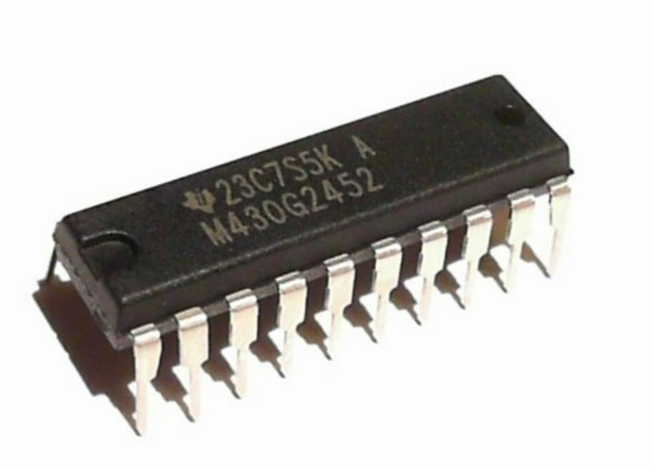
Recover Microcontroller 430G2452 Heximal
Our specialized service enables you to recover Microcontroller 430G2452 heximal code, helping you bypass locked or encrypted firmware and extract essential data. Whether your objective is to restore a legacy system, copy a failed firmware image, or clone a working configuration for backup or migration, our team provides safe and reliable solutions.
We employ advanced hardware-assisted techniques to crack and decode the protection mechanisms of the MCU. This includes overcoming secured fuse bits, accessing locked flash memory, and retrieving data from both program memory and EEPROM-like segments. Once unlocked, the extracted binary or heximal firmware is processed into readable source code or annotated assembly, depending on your need for analysis, porting, or documentation.
Recover Microcontroller 430G2452 Heximal out from MCU MSP430G2452 is a process start from Crack MCU MSP430G2452 protective system and disable its security fuse bit by focus ion beam, then copy the code fro new microcontroller;
FEATURES
Low Supply Voltage Range: 1.8 V to 3.6 V Ultra-Low Power Consumption
– Active Mode: 220 µA at 1 MHz, 2.2 V
– Standby Mode: 0.5 µA
– Off Mode (RAM Retention): 0.1 µA
Five Power-Saving Modes Ultra-Fast Wake-Up From Standby Mode in Less Than 1 µs 16-Bit RISC Architecture, 62.5-ns Instruction Cycle Time.
Basic Clock Module Configurations
– Internal Frequencies up to 16 MHz With
Four Calibrated Frequencies
– Internal Very-Low-Power Low-Frequency (LF) Oscillator
– 32-kHz Crystal
– External Digital Clock Source
One 16-Bit Timer_A With Three Capture/Compare Registers Up to 16 Touch-Sense Enabled I/O Pins
Universal Serial Interface (USI) Supporting SPI and I2C 10-Bit 200-ksps Analog-to-Digital (A/D)
Converter With Internal Reference, Sample-and-Hold, and Autoscan (MSP430G2x52 Only) On-Chip Comparator for Analog Brownout Detector Serial Onboard Programming, No External Programming Voltage Needed, Programmable Code Protection by Security Fuse On-Chip Emulation Logic With Spy-Bi-Wire Interface Family Members are Summarized:
Package Options
– TSSOP: 14 Pin, 20 Pin
– PDIP: 20 Pin
– QFN: 16 Pin
For Complete Module Descriptions, See the MSP430x2xx Family User’s Guide (SLAU144)
DESCRIPTION
The Texas Instruments MSP430™ family of ultra-low-power microcontrollers consist of several devices featuring different sets of peripherals targeted for various applications. The architecture, combined with five low-power modes, is optimized to achieve extended battery life in portable measurement applications.
The device features a powerful 16-bit RISC CPU, 16-bit registers, and constant generators that contribute to maximum code efficiency. The digitally controlled oscillator (DCO) allows wake-up from low-power modes to active mode in less than 1 µs.
The MSP430G2x52 and MSP430G2x12 series of microcontrollers are ultra-low-power mixed signal microcontrollers with built-in 16-bit timers, and up to 16 I/O touch sense enabled pins and built-in communication capability using the universal serial communication interface and have a versatile analog comparator.
The MSP430G2x52 series have a 10-bit A/D converter. For configuration details see Table 1. Typical applications include low-cost sensor systems that capture analog signals, convert them to digital values, and then process the data for display or for transmission to a host system when attacking Microcontrolle ST62T15C6 firmware memory.
Core Services Offered:
- Fuse Bit Bypass: Disable fuse protection to allow memory access.
- Firmware Extraction: Retrieve full program memory, eeprom, and configuration data.
- Binary/Heximal to Source: Convert raw memory dumps into readable C-like code or reconstruct assembly.
- Data Recovery: Recover lost or corrupted firmware from damaged or bricked units.
- System Cloning: Create functionally identical duplicates for hardware migration or replication.
- Security Testing: Evaluate your system’s resilience by simulating a penetration attempt into encrypted or protected MCUs.
Why Choose Us?
- Deep Expertise in MSP430 Architecture: We understand the protection mechanisms, memory layout, and debug interface of the 430G2452 inside-out.
- Confidential & Legal Compliance: Your data and intellectual property are handled securely, with strict confidentiality measures.
- Custom Reporting: We provide optional documentation outlining the structure, functions, and memory map of recovered program files or archives.
- Flexible Delivery: Whether you need a raw binary, disassembled listing, or decompiled source code, we deliver what fits your workflow.
Application Scenarios
MSP430G2452 is often deployed in wearable medical sensors, remote controls, industrial sensors, battery-operated meters, and consumer electronics. When the original source code is lost or the firmware becomes locked, our service ensures your product lifecycle doesn’t come to a halt. Recovering firmware from protected chips isn’t just about duplication—it’s about preserving investment, minimizing downtime, and enabling further innovation.