Archive for the ‘Break IC’ Category
 Noise Component is Power Consumption Characteristics
 February 2nd, 2013 |
  Author:
 Power consumption characteristics always include noise components. The external noise can be reduced by proper design of the signal acquisition path and careful use of the measurement equipment. Measuring the power consumption on the resistor in the ground line has some advantages. Firstly, it reduces the noise level and, secondly, it allows us to measure the signal directly with an oscilloscope probe, because most probes have their common line permanently connected to the main power ground. To increase the signal-to-noise ratio further, the number of averaged samples can be increased.
 Posted in Break IC |
  Tags: crack cpld mcu content, crack cpld mcu file, crack cpld mcu firmware, crack cpld mcu flash, crack cpld mcu program |
  Comments Closed
Simple power analysis (SPA) and Differential power analysis (DPA)
There are two major power analysis techniques – simple power analysis (SPA) and differential power analysis (DPA). SPA involves direct observation of the power consumption during cryptographic or other security sensitive operations. SPA can reveal information about the device’s operation as well as the key material. If the attacker knows the cryptographic algorithm (and especially its implementation in the tested device) he can easily work out some bits of information by observing the sequences of CPU instructions, especially rotation and conditional branches. If the result of an arithmetic or logic operation can be observed as well, i.e. the state of carry, zero or negative flags, more information can be obtained. DPA is a more powerful technique, because the attacker does not have to know as many details about how the cryptographic algorithm was implemented. It uses statistical analysis to extract hidden information from a large sample of power traces obtained during cryptographic computations with known ciphertexts. The statistical methods identify small differences in power consumption which can be used to recover individual bits in a secret key.
Posted in Break IC |
Tags: crack avr ic mcu bin code, crack avr ic mcu embeded firmware, crack avr ic mcu encrypt program, crack avr ic mcu flash content, crack avr ic mcu hex file, crack avr ic mcu software data |
Comments Closed
Different levels of activity in the instruction decoder and arithmetic units
The various instructions cause different levels of activity in the instruction decoder and arithmetic units, and can often be quite clearly distinguished so that parts of algorithms can be reconstructed. Various units of the processor have their switching transients at different times relative to the clock edges, and can be separated in high-frequency measurements.
There are many publications on different power analysis techniques that can be used to break many cryptographic algorithms. The whole process of analysis is relatively easy to implement, and only requires standard off-the-shelf measurement equipment costing a few thousand pounds.
Posted in Break IC |
Tags: cpld mcu bin, cpld mcu code, cpld mcu data, cpld mcu eprom, cpld mcu hex |
Comments Closed
Smaller Signals can be identified
By averaging the current measurements of many repeated identical operations, even smaller signals that are not transmitted over the bus can be identified. Signals such as carry-bit states are of special interest, because many cryptographic key-scheduling algorithms use shift operations that single out individual key bits in the carry flag. Even if the status-bit changes cannot be measured directly, they often cause changes in the instruction sequence or microcode execution, which then cause a clear change in the power consumption.
Computing Device Power Consumption
A computing device’s power consumption depends on its current activity. The consumption depends on changes of state of its components, rather than on the states themselves, because of the nature of CMOS transistors. When an input voltage is applied to a CMOS inverter, a transient short-circuit is induced. The rise of the current during this transient is much higher than the static dissipation caused by parasitic current leakage. Using a 10-20 resistor in the power supply line, these current fluctuations can be measured. To achieve good results, measurements should be made with at least 12-bit resolution and 50 MHz sampling frequency. Such acquisition parameters allow us to distinguish between different CPU instructions and estimate the number of bus bits changing at a time.
Break IC ATmega324V Protected Firmware
We can break IC ATMEGA324V protected firmware, please view the IC ATMEGA324V features for your reference:
The internal PLL in ATtiny15L generates a clock frequency that is 16x multiplied from the RC oscillator system clock. If the RC oscillator frequency is the nominal 1.6 MHz, the fast peripheral clock is 25.6 MHz.
The fast peripheral clock, or a clock prescaled from that, can be selected as the clock source for Timer/Counter1. The PLL is locked on the tunable internal RC oscillator and adjusting the tunable internal RC oscillator via the OSCCAL register will adjust the fast peripheral clock at the same time.
Timer1 may malfunction if the internal RC oscillator is adjusted beyond 1.75 MHz. It is recommended not to take the OSCCAL adjustments to a higher frequency than 1.75 MHz in order to keep proper operation of all chip functions before Break IC ATmega324V Protected Firmware.
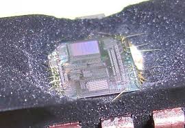
Break IC ATmega324V Protected Firmware
The ATmega324 provides two general purpose 8-bit Timer/Counters. The Timer/Counters hav e se par ate p re sc al ing s ele cti on fr om s epar at e 1 0- bit pres calers.
The Timer/Counter0 uses internal clock (CK) as the clock time base. The Timer/Counter1 may use either the internal clock (CK) or the fast peripheral clock (PCK) as the clock time base when break ic protected firmware.
The four prescaled selections are: CK/8, CK/64, CK/256, and CK/1024, where CK is the oscillator clock. CK, external source and stop, can also be selected as clock sources if Break IC ATmega324V Protected Firmware.
Setting the PSR10 bit in SFIOR resets the prescaler. This allows the user to operate with a predictable prescaler. Figure 19 shows the Timer/Counter1 prescaler.
For Timer/Counter1 the clock selections are: PCK, PCK/2, PCK/4, PCK/8, CK (=PCK/16), CK/2, CK/4, CK/8,CK/16, CK/32, CK/64, CK/128, CK/256, CK/512, CK/1024, and stop. The clock options are described in Table 12 on page 32 and the Timer/Counter1 Control Register (TCCR1).
Setting the PSR1 bit in the SFIOR register resets the 10-bit prescaler. This allows the user to operate with a predictable prescaler.
Avoid holes on security design
Any security system, either software or hardware, could also have holes in its design and there is always a small chance that an attacker would eventually find one with brute force random testing. Careful design of the security protection, followed by proper evaluation, could help avoid many problems and make such attacks virtually impossible.
Exploite Access Interface
The IC attacker could be also applied to the device communication protocol in order to find any hidden functions embedded by the software developer for testing and upgrade purposes. Chip manufacturers very often embed hardware test interfaces for postproduction testing of their semiconductor devices. If the security protection for these interfaces is not properly designed, the attacker can exploit it to get access to the on-chip memory. In smartcards such test interfaces are normally located outside the chip circuit and physically removed after the test operation, eliminating any possibility of use by outsiders.
Posted in Break IC |
Tags: exploit embeded content, exploit embeded firmware, exploit embeded program, exploit embeded software |
Comments Closed
Brute Force Eeprom Attack
Another possible brute force eeprom attack, applicable to many semiconductor chips, is applying an external high voltage signal (normally twice the power supply) to the chip’s eeprom pins to find out whether one of them has any transaction like entering into a factory test or programming mode. In fact, such pins can be easily found with a digital multimeter because they do not have a protection diode to the power supply line. Once sensitivity to a high voltage is found for any pin, the eeprom attacker can try a systematic search on possible combinations of logic signals applied to other pins to figure out which of them are used for the test/programming mode and exploit this opportunity.
Brute Force Chip Break Application
Brute force chip break can be also applied to a hardware design implemented into an ASIC or a CPLD. In this case the chip breaker tries to apply all possible logic combinations to the input of the device while observing all its outputs.
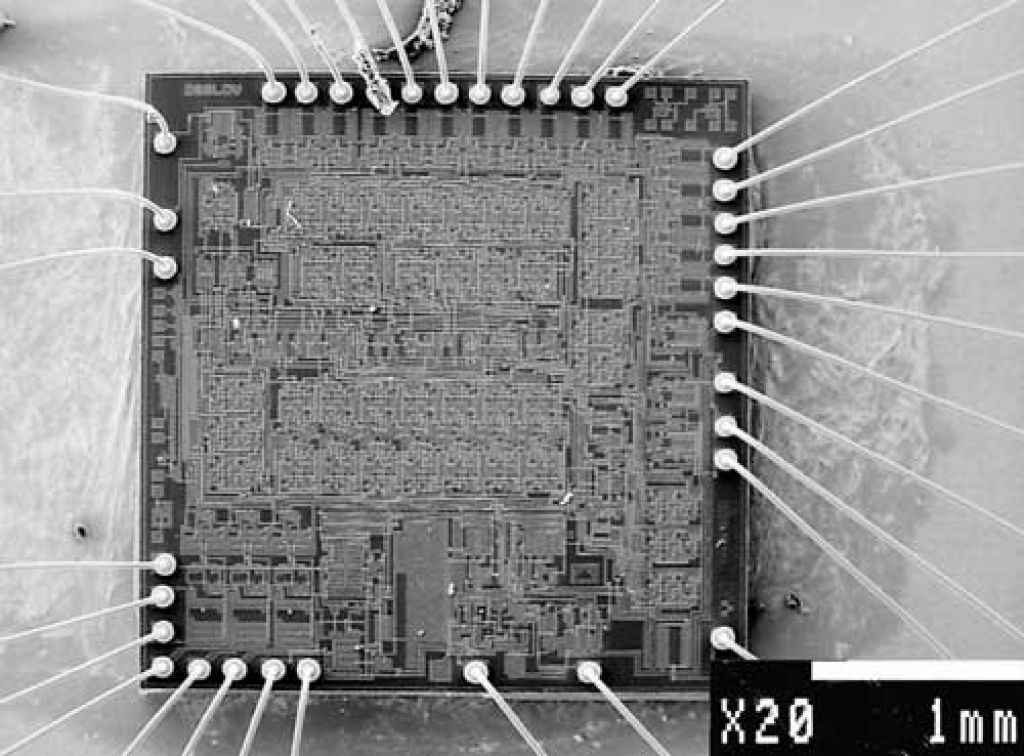
That kind of microcontroller breaking could be also called black-box analysis because the MCU cracker does not have to know anything about the design of the device under test.
He only tries to understand the function of the device by trying all possible combinations of signals. This approach works well only for relatively small logic devices. Another problem the MCU reading process will face is that designs implemented in CPLDs or ASICs have flip-flops, so the output will probably be function of both the previous state and the input.
But the search space can be significantly reduced if the signals are observed and analysed beforehand. For example, clock inputs, data buses and some control signals could be easily identified, significantly reducing the area of search.
Posted in Break IC |
Tags: Brute Force Chip attacking, brute force chip crack, Brute Force Chip decoding, Brute Force Chip reverse engineering |
Comments Closed