Archive for the ‘Break IC’ Category
 Attack Texas Instrument MSP430G2111 Microprocessor
 October 10th, 2020 |
  Author:
 Attack Texas Instrument MSP430G2111 Microprocessor and clone mcu msp430g2111 flash memory program from original MCU, copy binary firmware to new microcontroller;
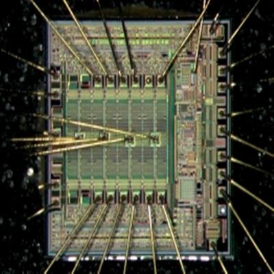
The flash memory can be programmed via the Spy-Bi-Wire/JTAG port or in-system by the CPU. The CPU can perform single-byte and single-word writes to the flash memory. Features of the flash memory include:
- Flash memory has n segments of main memory and four segments of information memory (A to D) of 64 bytes each. Each segment in main memory is 512 bytes in size.
- Segments 0 to n may be erased in one step, or each segment may be individually erased.
- Segments A to D can be erased individually or as a group with segments 0 to n. Segments A to D are also called information memory.
- Segment A contains calibration data. After reset segment A is protected against programming and erasing. It can be unlocked but care should be taken not to erase this segment if the device-specific calibration data is required.
 Posted in
Restore TI MCU MSP430G2101 Flash Content
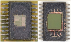
Restore TI MCU MSP430G2101 Flash Content starts from unlock microcontroller msp430g2101 flash memory, its protective system will be removed and embedded firmware of flash memory of processor MSP430G2 will be readout;
The interrupt vectors and the power-up starting address are located in the address range 0FFFFh to 0FFC0h. The vector contains the 16-bit address of the appropriate interrupt handler instruction sequence. If the reset vector (located at address 0FFFEh) contains 0FFFFh (e.g., flash is not programmed) the CPU will go into LPM4 immediately after power-up which can be used for microcontroller mixed signal msp430g2452 memory binary file restoration.
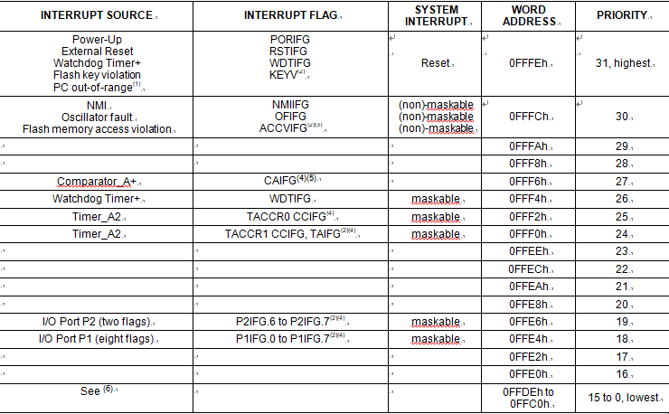
- A reset is generated if the CPU tries to fetch instructions from within the module register memory address range (0h to 01FFh) or from within unused address ranges.
- Multiple source flags
- (non)-maskable: the individual interrupt-enable bit can disable an interrupt event, but the general interrupt enable cannot.
- Interrupt flags are located in the module.
- Devices with Comparator_A+ only
- The interrupt vectors at addresses 0FFDEh to 0FFC0h are not used in this device and can be used for regular program code if necessary.
Replicate ARM MCU STM32F105R8T6 Embedded Flash Program
Replicate ARM MCU STM32F105R8T6 Embedded Flash Program and crack arm mcu protective fuse bit and then extract firmware from flash and eeprom memory of microprocessor;
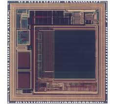
The ARM Cortex™-M3 processor is the latest generation of ARM processors for embedded systems. It has been developed to provide a low-cost platform that meets the needs of MCU implementation, with a reduced pin count and low-power consumption, while delivering outstanding computational performance and an advanced system response to interrupts of arm microcontroller stm32f105vct flash memory content decrypting.
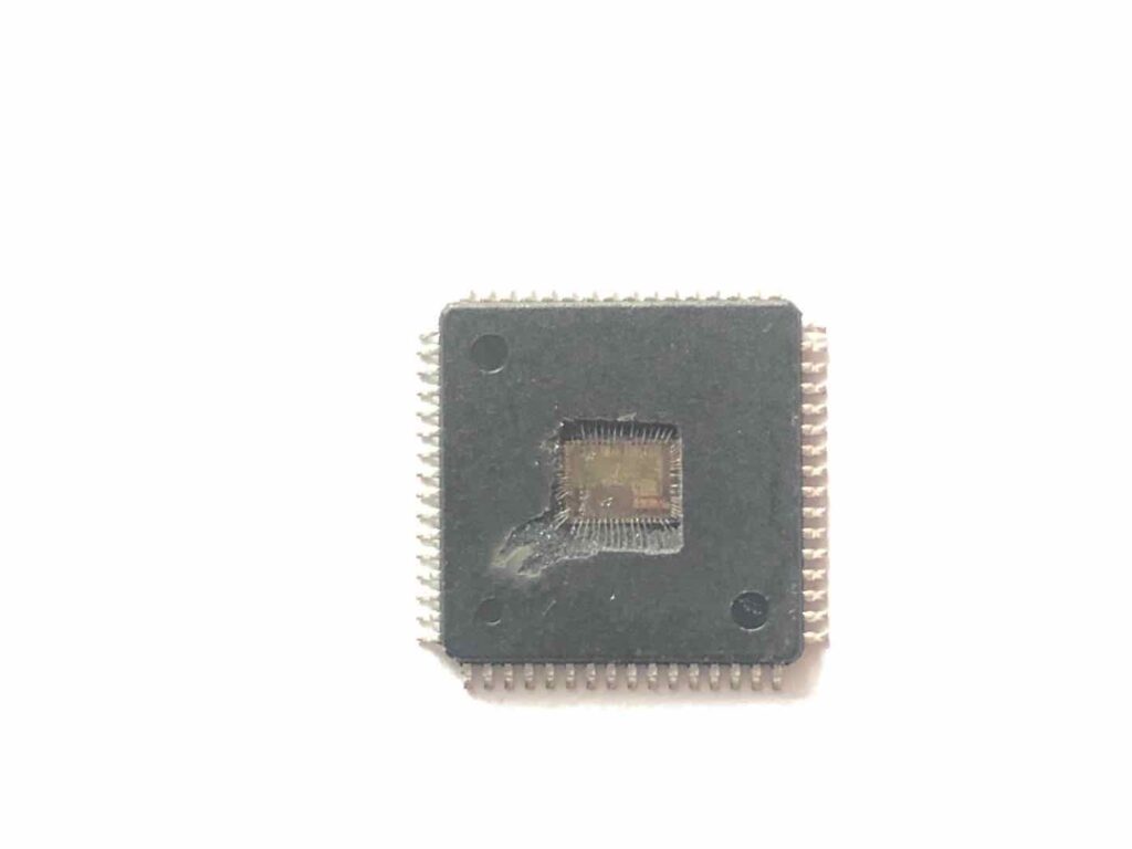
The ARM Cortex™-M3 32-bit RISC processor features exceptional code-efficiency, delivering the high-performance expected from an ARM core in the memory size usually associated with 8- and 16-bit devices.
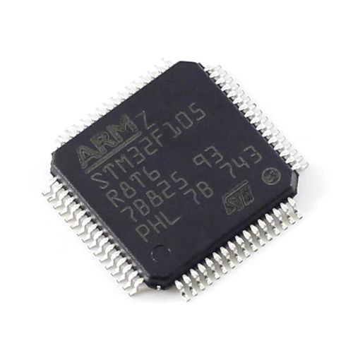
extract arm microprocessor stm32f105r8 source code from flash memory
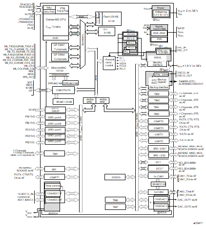
With its embedded ARM core, STM32F105xx and STM32F107xx connectivity line family is compatible with all ARM tools and software. below Figure shows the general block diagram of the device family.
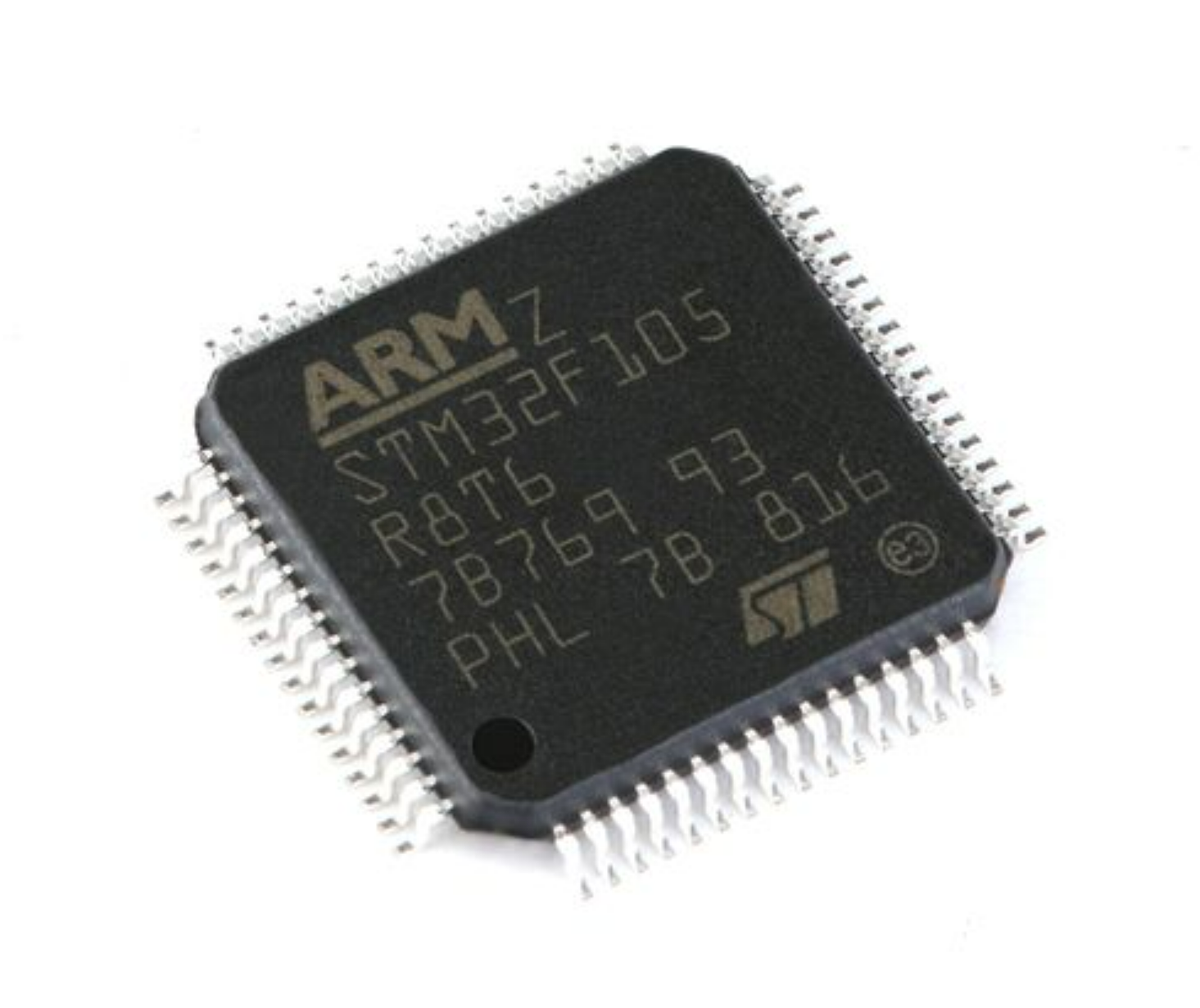
répliquer le programme flash intégré du MCU ARM STM32F105R8T6 et le bit de fusible de protection du MCU Crack Arm, puis extraire le micrologiciel de la mémoire flash et de la mémoire eeprom du microprocesseur ;
Decrypt ARM Microcontroller STM32F105VCT Secured Memory Binary Program
Decrypt ARM Microcontroller STM32F105VCT Secured Memory Binary Program is a process to unlock mcu stm32f105vct tamper resistance system, and then copy firmware from microprocessor;
Features
Core: ARM 32-bit Cortex™-M3 CPU
– 72 MHz maximum frequency, 1.25 DMIPS/MHz (Dhrystone 2.1) performance at 0 wait state memory
LQFP100 14 × 14 mm
LQFP64 10 × 10 mm access
– Single-cycle multiplication and hardware division Memories
– 64 to 256 Kbytes of Flash memory
– up to 64 Kbytes of general-purpose SRAM
Clock, reset and supply management
– 2.0 to 3.6 V application supply and I/Os
– POR, PDR, and programmable voltage detector (PVD)
– 3-to-25 MHz crystal oscillator
– Internal 8 MHz factory-trimmed RC
– Internal 40 kHz RC with calibration
– 32 kHz oscillator for RTC with calibration Low power
– Sleep, Stop and Standby modes
– VBAT supply for RTC and backup registers 2 × 12-bit, 1 µs A/D converters (16 channels)
– Conversion range: 0 to 3.6 V
– Sample and hold capability
– Temperature sensor
– up to 2 MSPS in interleaved mode 2 × 12-bit D/A converters
DMA: 12-channel DMA controller
– Supported peripherals: timers, ADCs, DAC, I2Ss, SPIs, I2Cs and USARTs
Up to 10 timers with pinout remap capability
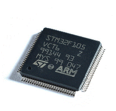
descifrar el microcontrolador ARM STM32F105VCT6 programa binario de memoria segura es un proceso para desbloquear el sistema de resistencia a manipulaciones MCU STM32F105VCT y luego copiar el firmware del microprocesador;
– Up to four 16-bit timers, each with up to 4 IC/OC/PWM or pulse counter and quadrature (incremental) encoder input
– 1 × 16-bit motor control PWM timer with dead-time generation and emergency stop
– 2 × watchdog timers (Independent and Window)
– SysTick timer: a 24-bit downcounter
– 2 × 16-bit basic timers to drive the DAC
Up to 14 communication interfaces with pinout remap capability
– Up to 2 × I2C interfaces (SMBus/PMBus)
– Up to 5 USARTs (ISO 7816 interface, LIN,
IrDA capability, modem control)
– Up to 3 SPIs (18 Mbit/s), 2 with a multiplexed I2S interface that offers audio class accuracy via advanced PLL schemes
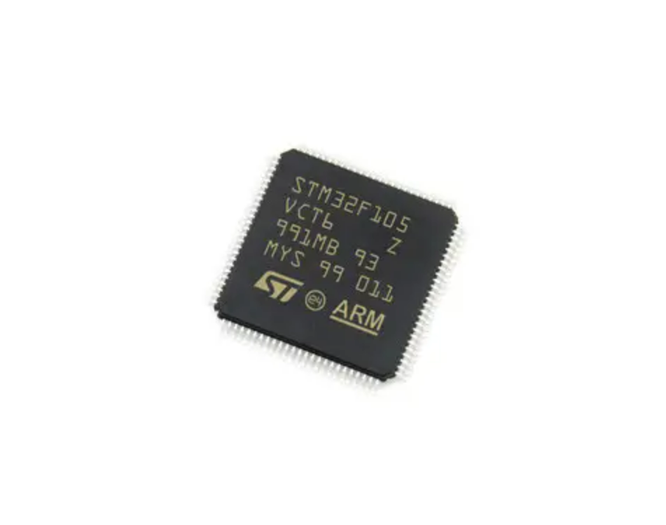
décrypter le microcontrôleur ARM STM32F105VCT6 programme binaire de mémoire sécurisée est un processus permettant de déverrouiller le système de résistance à l’effraction MCU STM32F105VCT, puis de copier le micrologiciel du microprocesseur ;
– 2 × CAN interfaces (2.0B Active) with 512 bytes of dedicated SRAM
– USB 2.0 full-speed device/host/OTG controller with on-chip PHY that supports HNP/SRP/ID with 1.25 Kbytes of dedicated SRAM
– 10/100 Ethernet MAC with dedicated DMA and SRAM (4 Kbytes): IEEE1588 hardware support, MII/RMII available on all packages
– Serial wire debug (SWD) & JTAG interfaces
Duplicate ARM MCU STM32F101CB Memory Content
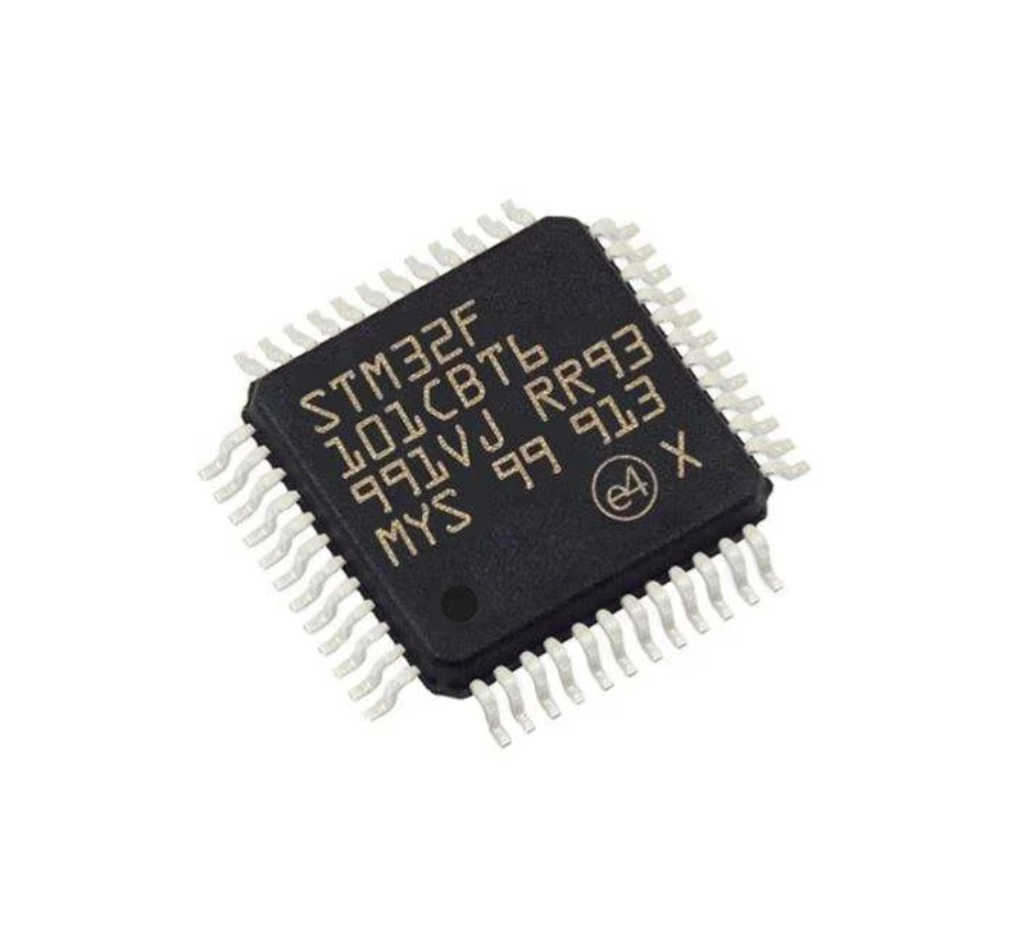
Duplicate ARM MCU STM32F101CB Memory Content include the program of locked flash memory and data of locked eeprom memory, the tamper resistance system of microcontroller stm32f101cb will be unlocked and embedded binary will extracted from MCU;
The advanced-control timer (TIM1) can be seen as a three-phase PWM multiplexed on 6 channels which can provide great benefit to Unlock ARM Base STM32F101CB Microprocessor. It has complementary PWM outputs with programmable inserted dead times to Copy microcontroller. It can also be seen as a complete general-purpose timer. The 4 independent channels can be used for:
il contenuto della memoria STM32F101CB dell’MCU ARM duplicato include il programma della memoria flash bloccata e i dati della memoria eeprom bloccata, il sistema di resistenza alle manomissioni del microcontrollore stm32f101cb verrà sbloccato e il binario incorporato verrà estratto dall’MCU;
- Input capture
- Output compare
- PWM generation (edge or center-aligned modes)
- One-pulse mode output
The counter can be frozen in debug mode. Many features are shared with those of the standard TIM timers which have the same architecture. The advanced control timer can therefore work together with the TIM timers via the Timer Link feature for synchronization or event chaining to facilitate the progress of recovering locked Microcontroller stm32f101c4 embedded firmware.
There are six synchronizable general-purpose timers embedded in the STM32F100xx devices. Each general-purpose timers can be used to generate PWM outputs, or as simple time base. STM32F100xx devices feature three synchronizable 4-channels general-purpose timers.
дубльований вміст пам’яті ARM MCU STM32F101CB включає програму заблокованої флеш-пам’яті та дані заблокованої пам’яті eeprom, систему захисту від несанкціонованого доступу мікроконтролера STM32F101CB буде розблоковано, а вбудований двійковий файл буде витягнуто з MCU;
These timers are based on a 16-bit auto-reload up/downcounter and a 16-bit prescaler. They feature 4 independent channels each for input capture/output compare, PWM or one-pulse mode output. This gives up to 12 input captures/output compares/PWMs on the largest packages.
Break ARM Microcontroller STM32F101RB Flash Memory
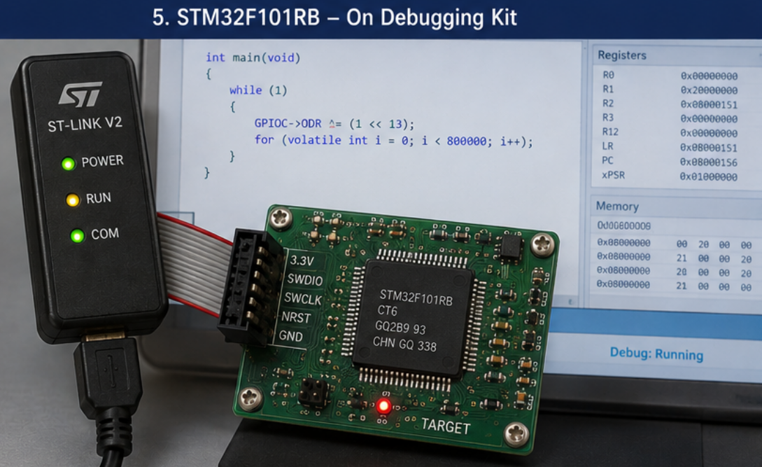
The STM32F101RB microcontroller represents an incredibly robust and versatile piece of silicon architecture, engineered on a 32-bit ARM Cortex-M3 processor core running up to 36 MHz. This highly reliable device is frequently integrated as the central execution engine within mission-critical utility grid systems, clinical medical apparatus, smart barcode scanners, and intricate environmental control sub-assemblies. Featuring distinct peripheral parameters like its 7-channel DMA controller, 12-bit Analog-to-Digital converters, and an array of communication interfaces such as USART, I2C, and SPI, this chip excels at processing real-time telemetry. Its embedded firmware is housed in a high-density, on-chip storage area designed to keep proprietary device logic running autonomously for decades. However, industrial businesses frequently run into immediate production roadblocks when a legacy platform must be serviced or migrated, but the initial documentation, source code files, or master engineering libraries have been completely lost to time. When critical components become obsolete or supplier access vanishes, establishing a trustworthy mechanism to read out the internal configuration becomes a major priority. Our elite laboratory specializes in precision hardware manipulation designed to break ARM Microcontroller STM32F101RB Flash Memory architectures, providing a trusted option to recover your original design assets.
The TIM2, TIM3, TIM4 general-purpose timers can work together or with the TIM1 advanced-control timer via the Timer Link feature for synchronization or STMicro STM32F101RB MCU Cracking.
TIM2, TIM3, TIM4 all have independent DMA request generation.
These timers are capable of handling quadrature (incremental) encoder signals and the digital outputs from 1 to 3 hall-effect sensors. Their counters can be frozen in debug mode. Overcoming the high-grade internal security layout of an enterprise-level microcontroller requires navigating sophisticated hardware-level reading barriers natively deployed to shield proprietary software assets. To carefully attack, break, and decode these complex internal hardware-level locks, our engineering lab implements a rigorous, non-destructive physical and electrical procedure.
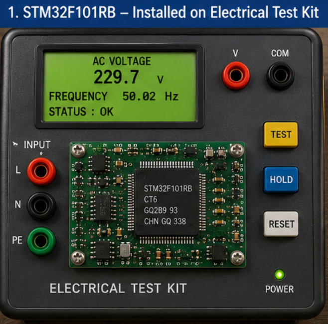
Tescilli kontrol kodunuz eski bir çevresel PLD matrisi içinde, harici bellek yongalarında veya doğrudan ARM STM32F101RB mikrodenetleyicisinin çekirdek mikro mimarisinde bulunuyor olsun, özel okuma araçlarımız operasyonel verilerin eksiksiz bir kopyasını güvenli şekilde elde edebilir.
Ekibimiz ham veri akışını başarıyla geri aldıktan sonra, mühendisler tam operasyonel parametreleri modern ve kolay temin edilebilen bir ARM STM32F101RB mikrodenetleyicisine aktarabilir. Bu kapsamlı veri çıkarma süreci, orijinal cihaz davranışının aynı şekilde yeniden oluşturulmasını sağlar.
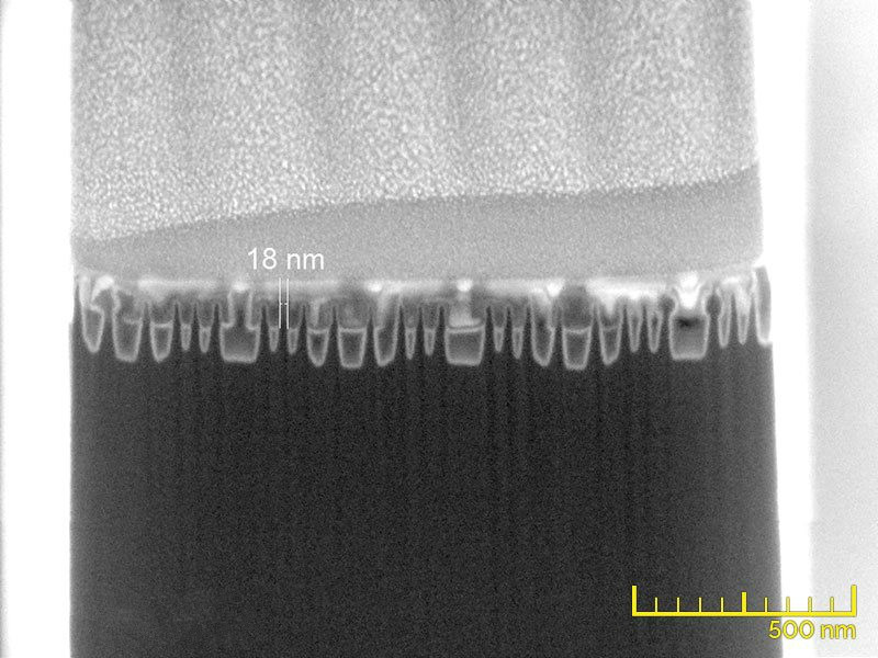
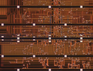
Initially, specialized technicians decapsulate the outer epoxy molding of the integrated circuit with chemical precision, exposing the bare silicon die and its sub-micron layout underneath. Once the internal structures are fully visible under advanced microscopic imaging, we can analyze the status of the embedded protective code fuses. By utilizing deep-precision micro-probing techniques or targeted optical signal modification directly on the physical registers, our team can carefully bypass the internal security bits that restrict reading access via the JTAG or Serial Wire Debug ports. This precise intervention allows us to extract the completely untouched binary data straight from the inner flash and protected eeprom sectors without corrupting the physical substrate. The definitive deliverable from this advanced engineering operation is a completely pristine, uncorrupted heximal file that contains a flawless structural mirror of your system’s original configuration.
The TIM15, TIM16 and TIM17 timers can work together, and TIM15 can also operate with TIM1 via the Timer Link feature for synchronization or event chaining. TIM15 can be synchronized with TIM16 and TIM17.
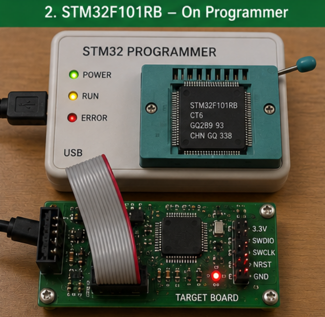
TIM15, TIM16, and TIM17 have a complementary output with dead-time generation and independent DMA request generation Their counters can be frozen in debug mode. These timers are mainly used for DAC trigger generation. They can also be used as a generic 16-bit time base. The fundamental purpose of choosing to hack, duplicate, or extract code from a heavily secured microcontroller layout is to eliminate single-point supply chain failures and secure a company’s long-term technical autonomy.
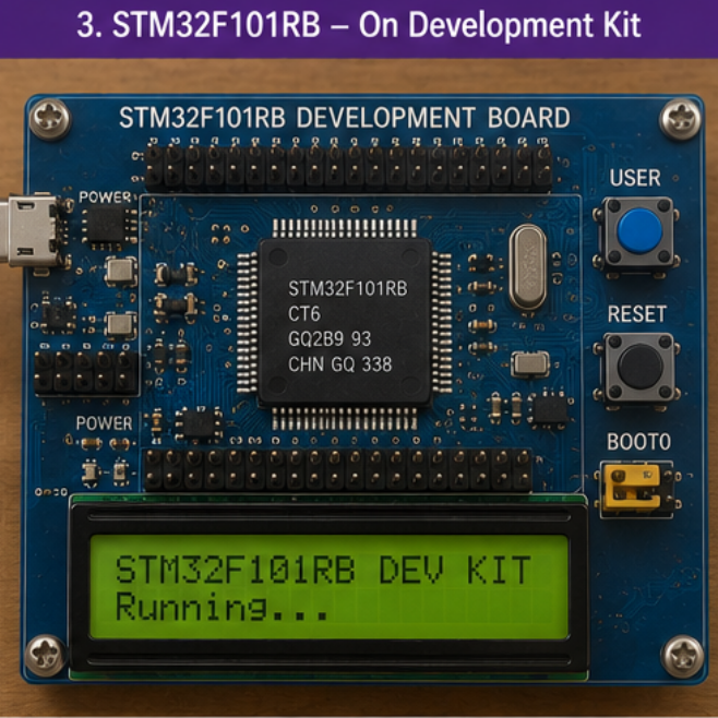
When engineering teams lose access to their original program archive, our advanced laboratory recovery techniques provide an efficient way to recover the vital machinery instructions before a full-scale, incredibly expensive system redesign is forced upon your budget. Whether your proprietary control code is isolated inside an older peripheral PLD matrix, external memory chips, or the core micro-architecture of the ARM chip itself, our custom reading tools can extract the complete operational file safely. After our team successfully retrieves the raw data stream, engineers can easily clone the full operational parameters onto a modern, readily available replacement microcontroller. This comprehensive data extraction allows you to duplicate the original device behavior exactly, giving your manufacturing team a clean, verified engineering archive to resume board production without risking a single day of system downtime.
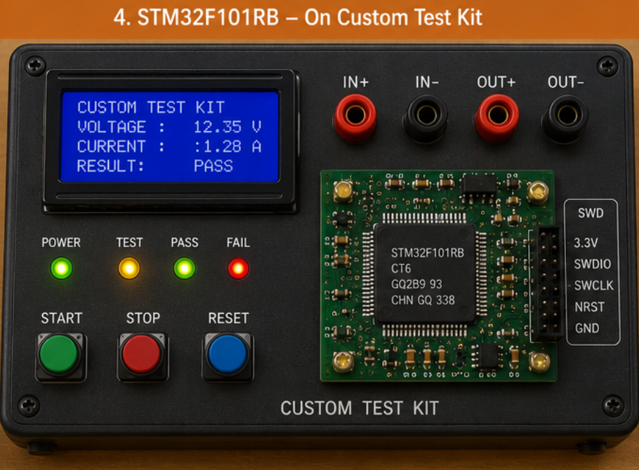
Partnering with an experienced technical team to unlock and recover embedded system software delivers major financial, operational, and strategic benefits to project managers, maintenance engineers, and hardware developers alike. Instead of exhausting immense corporate capital and spending quarters of valuable engineering time trying to reverse-engineer and re-write complex embedded applications from scratch—a risky process that notorious introduces hidden software bugs—our advanced extraction pipeline delivers a fast, precise path to a fully verified binary file. This complete structural continuity ensures that every newly generated duplicate circuit board matches the exact performance and behavioral profile of the field-tested units your clients already trust. By utilizing our specialized microcontroller recovery solutions, your enterprise effectively mitigates the existential threats of part obsolescence, safeguards vital corporate intellectual property, and secures a fully predictable roadmap for your industrial hardware investments for many years to come.
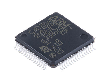
Attack Locked STM32F100R8 ARM MCU Flash Memory
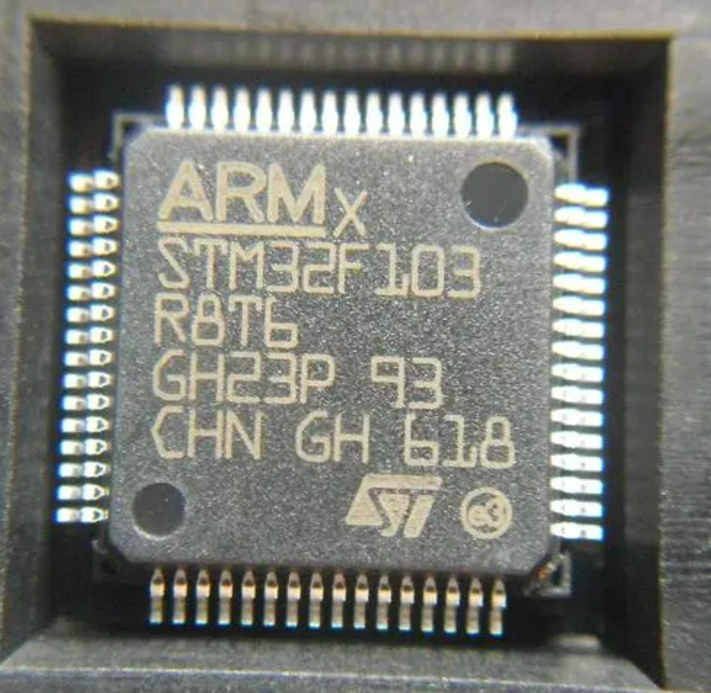
Attack Locked STM32F100R8 ARM MCU Flash Memory to extract microcontroller source code, and make microcontroller stm32f100r6 embedded firmware cloning;
STM32F100R8 power supply scheme will greatly improve the success rate of from its memory, hereby we will discuss and have better understanding about this process:
VDD = 2.0 to 3.6 V: External power supply for I/Os and the internal regulator. Provided externally through VDD
VSSA, VDDA = 0 to 3.6 V: External analog power supplies for ADC, Reset blocks, RCs and PLL (minimum voltage to be applied to VDDA is 2.4 V when the ADC is used). VDDA and VSSA must be connected to VDD and VSS, respectively.
هجوم مقفل STM32F100R8 ذاكرة فلاش ARM MCU لاستخراج شفرة مصدر متحكم ، وجعل متحكم stm32f100r6 جزءا لا يتجزأ من استنساخ البرامج الثابتة ؛
VBAT = 1.8 to 3.6 V: Power supply for RTC, external clock 32 kHz oscillator and backup registers (through power switch) when VDD is not present.
The device has an integrated power on reset (POR)/power down reset (PDR) circuitry. It is always active, and ensures proper operation starting from/down to 2 V. The device remains in reset mode when VDD is below a specified threshold, VPOR/PDR, without the need for an external reset circuit to facilitate the process of arm CPU stm32f100r8 flash memory breaking.
The device features an embedded programmable voltage detector (PVD) that monitors the VDD/VDDA power supply and compares it to the VPVD threshold. An interrupt can be generated when VDD/VDDA drops below the VPVD threshold and/or when VDD/VDDA is higher than the VPVD threshold. The interrupt service routine can then generate a warning message and/or put the MCU into a safe state. The PVD is enabled by software.
माइक्रोकंट्रोलर स्रोत कोड निकालने के लिए एआरएम एमसीयू फ्लैश मेमोरी STM32F100R8 हमला बंद, और माइक्रोकंट्रोलर STM32F100R8 एम्बेडेड फर्मवेयर क्लोनिंग बनाना;
The regulator has three operation modes: main (MR), low power (LPR) and power down.
- l MR is used in the nominal regulation mode (Run)
- l LPR is used in the Stop mode
- l Power down is used in Standby mode: the regulator output is in high impedance: the kernel circuitry is powered down, inducing zero consumption (but the contents of the registers and SRAM are lost)
This regulator is always enabled after reset to Break IC. It is disabled in Standby mode, providing high impedance output.
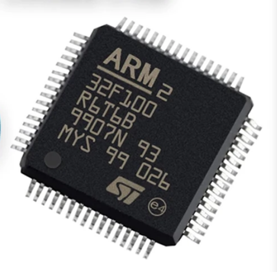
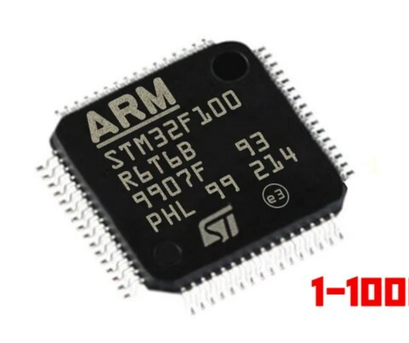
ARM Microcontroller STM32F100R6 Secured Flash Breaking
ARM Microcontroller STM32F100R6 Secured Flash Breaking needs to remove the security fuse bit protection over its flash and eeprom memory and readout the embedded firmware from locked processor;
STM32F100R6 power supply scheme will greatly improve the success rate of ARM Microcontroller STM32F100R6 Secured Flash Breaking, hereby we will discuss and have better understanding about this process:
VDD = 2.0 to 3.6 V: External power supply for I/Os and the internal regulator. Provided externally through VDD
VSSA, VDDA = 0 to 3.6 V: External analog power supplies for ADC, Reset blocks, RCs and PLL (minimum voltage to be applied to VDDA is 2.4 V when the ADC is used). VDDA and VSSA must be connected to VDD and VSS, respectively to execute Microchip PIC18LF452 MCU Code Cloning.
VBAT = 1.8 to 3.6 V: Power supply for RTC, external clock 32 kHz oscillator and backup registers (through power switch) when VDD is not present.
يحتاج متحكم ARM STM32F100R6 كسر الفلاش الآمن إلى إزالة حماية بت الصمامات الأمنية عبر فلاش STM32F100R6 MCU وذاكرة eeprom وقراءة البرامج الثابتة المضمنة من المعالج الدقيق المقفل واستنساخ شريحة MCU ؛
The device has an integrated power on reset (POR)/power down reset (PDR) circuitry. It is always active, and ensures proper operation starting from/down to 2 V. The device remains in reset mode when VDD is below a specified threshold, VPOR/PDR, without the need for an external reset circuit to facilitate the process of Restore DSP CPU TMS320F28030PAGT Source Code.
The device features an embedded programmable voltage detector (PVD) that monitors the VDD/VDDA power supply and compares it to the VPVD threshold. An interrupt can be generated when VDD/VDDA drops below the VPVD threshold and/or when VDD/VDDA is higher than the VPVD threshold for the purpose of Copy ARM MCU STMicroelectronics STM32F107RCT6. The interrupt service routine can then generate a warning message and/or put the MCU into a safe state. The PVD is enabled by software.
एआरएम माइक्रोकंट्रोलर STM32F100R6 सुरक्षित फ्लैश ब्रेकिंग को एमसीयू की STM32F100R6 फ्लैश और ईप्रोम मेमोरी पर सुरक्षा फ्यूज बिट सुरक्षा को हटाने और लॉक किए गए माइक्रोप्रोसेसर और क्लोन एमसीयू चिप से एम्बेडेड फर्मवेयर को पढ़ने की आवश्यकता है;
The regulator has three operation modes: main (MR), low power (LPR) and power down.
- l MR is used in the nominal regulation mode (Run)
- l LPR is used in the Stop mode
- l Power down is used in Standby mode: the regulator output is in high impedance: the kernel circuitry is powered down, inducing zero consumption (but the contents of the registers and SRAM are lost)
This regulator is always enabled after reset to Break IC. It is disabled in Standby mode, providing high impedance output.
Reverse Engineer STMicrco ARM MCU STM32F100C6
Reverse Engineer STMicrco ARM MCU STM32F100C6 needs to unlock stm32f100c6’s security fuse bit and then extract embedded firmware from microcontroller’s flash and eeprom memory;
The STM32F100xx value line family incorporates the high-performance ARM Cortex™-M3 32-bit RISC core operating at a 24 MHz frequency which will be useful for Unlock ARM MCU STM32F100C6 Memory, high-speed embedded memories (Flash memory up to 128 Kbytes and SRAM up to 8 Kbytes), and an extensive range of enhanced peripherals and I/Os connected to two APB buses.
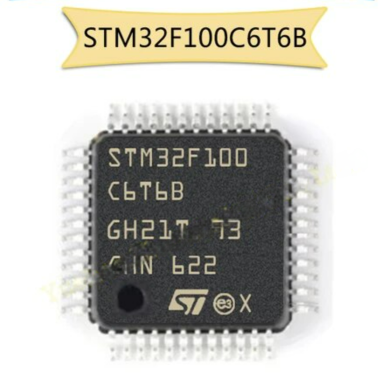
रिवर्स इंजीनियरिंग एसटीमाइक्रोको एआरएम एमसीयू STM32F100C6 को STM32F100C6 के सुरक्षा फ्यूज बिट को अनलॉक करने और फिर माइक्रोकंट्रोलर के फ्लैश और ईप्रोम मेमोरी से एम्बेडेड फर्मवेयर निकालने, समीपस्थ या बाइनरी के फर्मवेयर स्रोत कोड को नए माइक्रोकंट्रोलर STM32F100C6 में कॉपी करने की आवश्यकता होती है;
All devices offer standard communication interfaces (up to two I2Cs, two SPIs, one HDMI CEC, and up to three USARTs), one 12-bit ADC, two 12-bit DACs, up to six general-purpose 16-bit timers and an advanced-control PWM timer for the purpose of MCU source code reverse engineering.
The STM32F100xx low- and medium-density value line family operates in the –40 to +85 °C and –40 to +105 °C temperature ranges, from a 2.0 to 3.6 V power supply. A comprehensive set of power-saving mode allows the design of low-power applications.
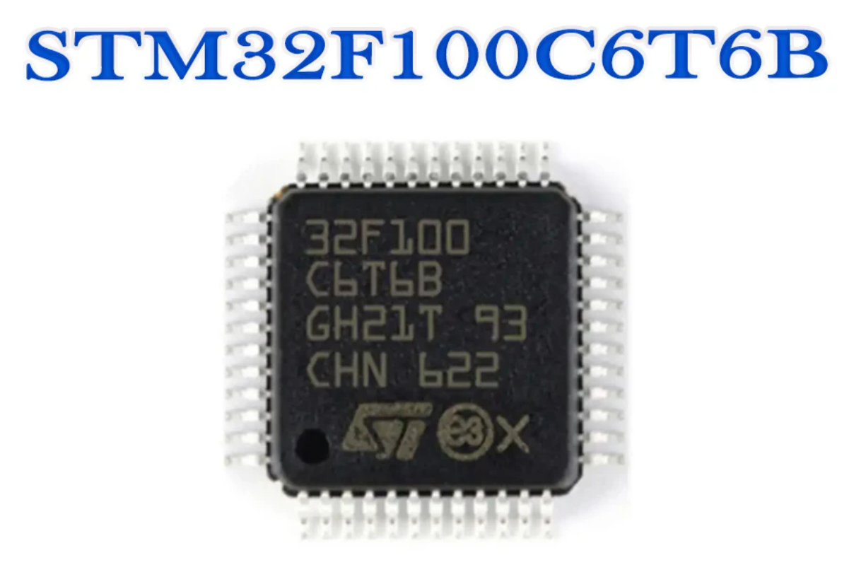
الهندسة العكسية STMicrco ARM MCU STM32F100C6 يحتاج إلى فتح بت الصمامات الأمنية STM32F100C6 ثم استخراج البرامج الثابتة المضمنة من فلاش متحكم دقيق وذاكرة EEPROM ، ونسخ شفرة مصدر البرامج الثابتة من heximal أو ثنائي إلى متحكم دقيق جديد STM32F100C6 ؛
The STM32F100xx value line family includes devices in three different packages ranging from 48 pins to 100 pins. Depending on the device chosen, different sets of peripherals are included, the description below gives an overview of the complete range of peripherals proposed in this family from the process of Crack Microcontroller IC TI 430G2452.
These features make the STM32F100xx value line microcontroller family from the process of Attack Microcontroller MCU Microchip PIC16F84A suitable for a wide range of applications:
Application control and user interface
Medical and handheld equipment
PC peripherals, gaming and GPS platforms
Industrial applications: PLC, inverters, printers, and scanners
Alarm systems, Video intercom, and HVAC
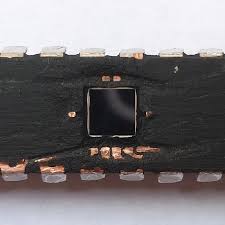
Attack Renesas R5F51115ADFM#3A MCU Flash Memory
Attack Renesas R5F51115ADFM#3A MCU Flash Memory and extract embedded binary from microcontroller flash memory and download it to new MCU for cloning purpose;
During sleep mode or mode transitions, do not write to the system control related registers (indicated by ‘SYSTEM’ in the Module Symbol column in Table 4.1, List of I/O Registers (Address Order)).
Permanent damage to the MCU may result if absolute maximum ratings are exceeded.
To preclude any malfunctions due to noise interference, insert capacitors of high frequency characteristics between the VCC and VSS pins, between the AVCC0 and AVSS0 pins, between the VCC_USB and VSS_USB pins, and between the VREFH0 and VREFL0 pins.
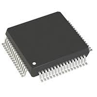
атакувати флеш-пам’ять MCU Renesas R5F51115ADFM#3A і витягти вбудовану двійкову або шістнадцяткову програмну прошивку з флеш-пам’яті мікроконтролера R5F51115ADFM#3A і скопіювати її в новий MCU з метою клонування;
Place capacitors of about 0.1 μF as close as possible to every power supply pin and use the shortest and heaviest possible traces. Also, connect capacitors as stabilization capacitance which will help to facilitate the process of cracking renesas mcu r5f563nfddf flash memory.
Connect the VCL pin to a VSS pin via a 4.7 μF capacitor. The capacitor must be placed close to the pin, refer to section 5.12.1, Connecting VCL Capacitor and Bypass Capacitors.
Do not input signals or an I/O pull-up power supply to ports other than 5-V tolerant ports while the device is not powered. The current injection that results from input of such a signal or I/O pull-up may cause malfunction and the abnormal current that passes in the device at this time may cause degradation of internal elements.
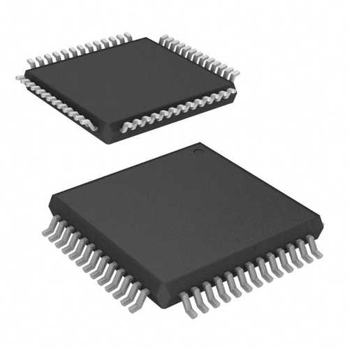
Renesas R5F51115ADFM#3A MCU flash belleğe saldırın ve mikrodenetleyici R5F51115ADFM#3A flash bellekten gömülü ikili veya onaltılık program bellenimini çıkarın ve klonlama amacıyla yeni MCU’ya kopyalayın;
If input voltage (within the specified range from -0.3 to + 6.5V) is applied to 5-V tolerant ports, it will not cause problems such as damage to the MCU.