Archive for April, 2010
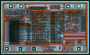
 Recover Chip PIC12C508 Software
Recover Chip PIC12C508 Software needs to firstly extract locked code from mcu pic12c508 mcu and then copy the embedded heximal to new microcontroller pic12c508;
High-Performance RISC CPU:
· Only 33 single word instructions to learn
· All instructions are single cycle (1 µs) except for program branches which are two-cycle
· Operating speed: DC – 4 MHz clock input DC – 1 µs instruction cyc
12-bit wide instructions
8-bit wide data path
Seven special function hardware registers
Two-level deep hardware stack
Direct, indirect and relative addressing modes for data and instructions
· Internal 4 MHz RC oscillator with programmable calibration
· In-circuit serial programming
· 8-bit real time clock/counter (TMR0) with 8-bit programmable prescaler
· Power-On Reset (POR)
· Device Reset Timer (DRT)
· Watchdog Timer (WDT) with its own on-chip RC oscillator for reliable operation
· Programmable code-protection
· 1,000,000 erase/write cycle EEPROM data memory
· EEPROM data retention > 40 years
· Power saving SLEEP mode
· Wake-up from SLEEP on pin change
· Internal weak pull-ups on I/O pins
· Internal pull-up on MCLR pin
· Selectable oscillator options:
– INTRC: Internal 4 MHz RC oscillator
– EXTRC: External low-cost RC oscillator
– XT: Standard crystal/resonator
– LP: Power saving, low frequency crystal
CMOS Technology:
· Low power, high speed CMOS EPROM/ROM technology
· Fully static design
· Wide operating voltage range
· Wide temperature range:
– Commercial: 0°C to +70°C
– Industrial: -40°C to +85°C
– Extended: -40°C to +125°C
· Low power consumption
– < 2 mA @ 5V, 4 MHz
Circuit Engineering Company Limited continues to be recognized as the Southern China Leader in Services for IC Read, MCU Crack, Chip Extract, Microcontroller Recover service.
With the advancement of today’s modern circuit board technology, it is more important than ever to have specialists available to help you at a moment’s notice. Our engineering and commercial teams collectively have a vast amount of electronic experience covering field include Consumer Electronics, Industrial Automation Electronics, Wireless Communication Electronics., etc. For more information please contact us through email.
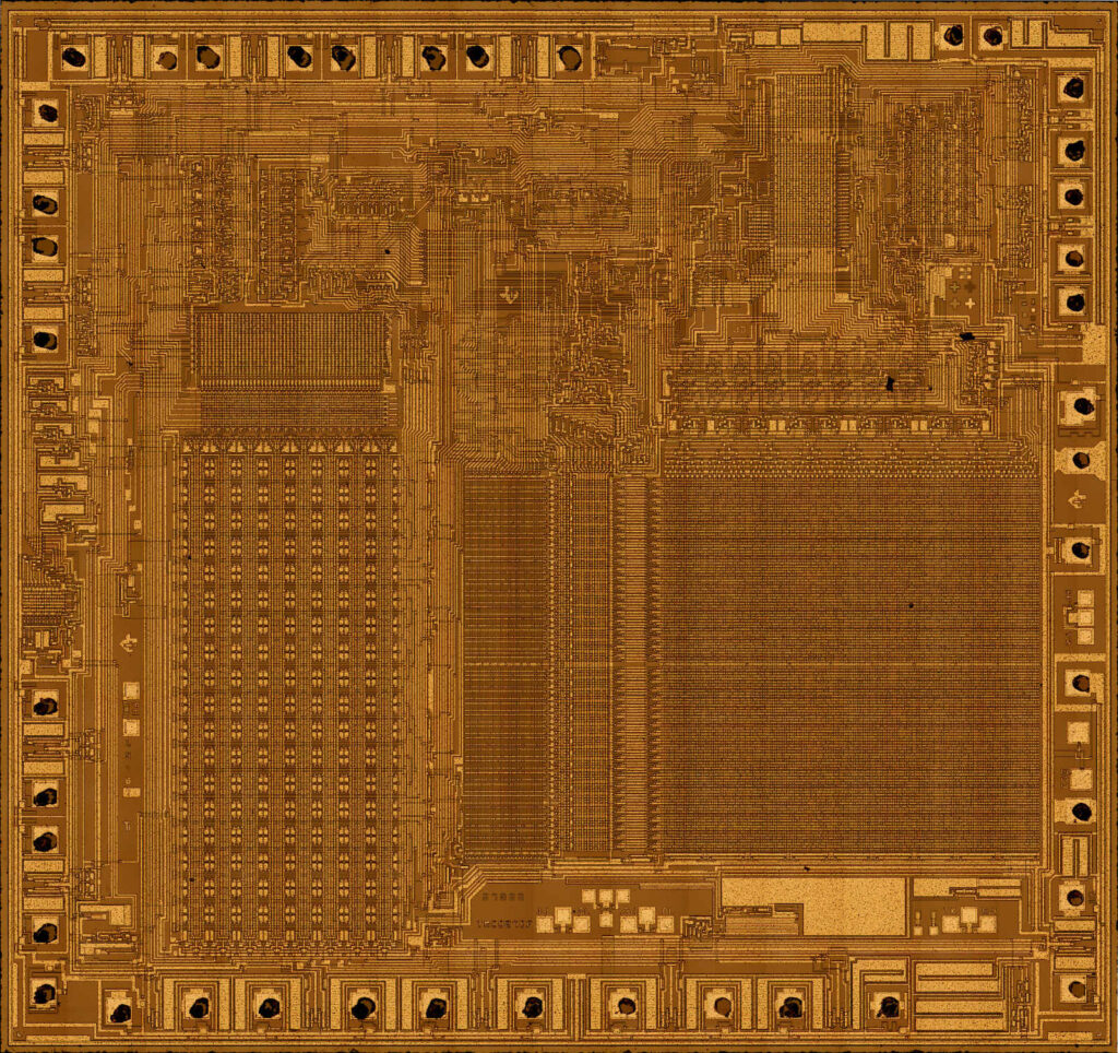
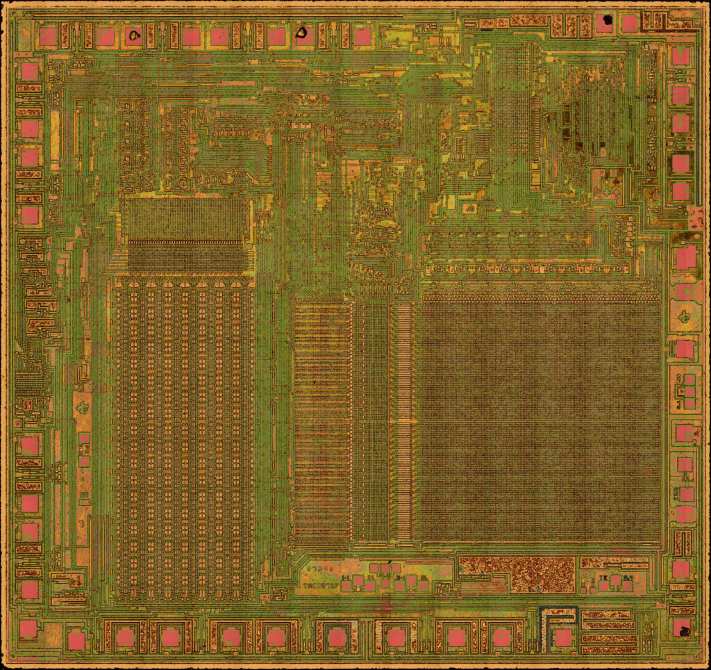
Break MCU ATmega2560L Flash
Break MCU ATmega2560L Flash memory and crack microcontroller atmega2560L fuse bit, read embedded heximal code out from MCU ATmega2560L flash memory;
The Timer/Counter can be clocked by an internal synchronous or an external asynchronous clock source. The clock source clkT2 is by default equal to the MCU clock, clkI/O.
When the AS2 bit in the ASSR Register is written to logic one, the clock source is taken from the Timer/Counter Oscillator connected to TOSC1 and TOSC2. For details on asynchronous operation, see “Asynchronous Status Register – ASSR” on page 189 if recover pic16c554 MCU software.
For details on clock sources and prescaler, see “Timer/Counter Prescaler” on page 193. The main part of the 8-bit Timer/Counter is the programmable bi-directional counter unit.
Figure 68 shows a block diagram of the counter and its surrounding environment. Depending on the mode of operation used, the counter is cleared, incremented, or decremented at each timer clock (clkT2). clkT2 can be generated from an external or internal clock source, selected by the Clock Select bits (CS22:0) before recover pic16f83 Mcu flash.
When no clock source is selected (CS22:0 = 0) the timer is stopped. However, the TCNT2 value can be accessed by the CPU, regardless of whether clkT2 is present or not. A CPU write overrides (has priority over) all counter clear or count operations.
The counting sequence is determined by the setting of the WGM21 and WGM20 bits located in the Timer/Counter Control Register (TCCR2A) and the WGM22 located in the Timer/Counter Control Register B (TCCR2B).
There are close connections between how the counter behaves (counts) and how waveforms are generated on the Output Compare outputs OC2A and OC2B. For more details about advanced counting sequences and waveform generation, see “Modes of Operation” on page 178.
The Timer/Counter Overflow Flag (TOV2) is set according to the mode of operation selected by the WGM22:0 bits. TOV2 can be used for generating a CPU interrupt.
The 8-bit comparator continuously compares TCNT2 with the Output Compare Register (OCR2A and OCR2B). Whenever TCNT2 equals OCR2A or OCR2B, the comparator signals a match. A match will set the Output Compare Flag (OCF2A or OCF2B) at the next timer clock cycle.
If the corresponding interrupt is enabled, the Output Compare Flag generates an Output Compare interrupt. The Output Compare Flag is automatically cleared when the interrupt is executed.
Alternatively, the Output Compare Flag can be cleared by software by writing a logical one to its I/O bit location. The Waveform Generator uses the match signal to generate an output according to operating mode set by the WGM22:0 bits and Compare Output mode (COM2x1:0) bits. The max and bottom signals are used by the Waveform Generator for handling the special cases of the extreme values in some modes of operation (“Modes of Operation” on page 178). Figure 58 on page 154 shows a block diagram of the Output Compare unit.
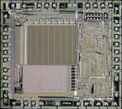
Reverse Engineering Chip ATmega2560L Software
Reverse Engineering Chip ATmega2560L Software is actually a process to read encrypted heximal from mcu atmega2560L flash memory after crack microcontroller atmega2560L security fuse bit;
The Timer/Counter can be clocked by an internal synchronous or an external asynchronous clock source. The clock source clkT2 is by default equal to the MCU clock, clkI/O.
When the AS2 bit in the ASSR Register is written to logic one, the clock source is taken from the Timer/Counter Oscillator connected to TOSC1 and TOSC2. For details on asynchronous operation, see “Asynchronous Status Register – ASSR” on page 189 if attack attiny2313 mcu firmware.
For details on clock sources and prescaler, see “Timer/Counter Prescaler” on page 193. The main part of the 8-bit Timer/Counter is the programmable bi-directional counter unit.
Figure 68 shows a block diagram of the counter and its surrounding environment. Depending on the mode of operation used, the counter is cleared, incremented, or decremented at each timer clock (clkT2). clkT2 can be generated from an external or internal clock source, selected by the Clock Select bits (CS22:0) before attack atmega64l mcu flash.
When no clock source is selected (CS22:0 = 0) the timer is stopped. However, the TCNT2 value can be accessed by the CPU, regardless of whether clkT2 is present or not. A CPU write overrides (has priority over) all counter clear or count operations.
The counting sequence is determined by the setting of the WGM21 and WGM20 bits located in the Timer/Counter Control Register (TCCR2A) and the WGM22 located in the Timer/Counter Control Register B (TCCR2B).
There are close connections between how the counter behaves (counts) and how waveforms are generated on the Output Compare outputs OC2A and OC2B. For more details about advanced counting sequences and waveform generation, see “Modes of Operation” on page 178.
The Timer/Counter Overflow Flag (TOV2) is set according to the mode of operation selected by the WGM22:0 bits. TOV2 can be used for generating a CPU interrupt.
The 8-bit comparator continuously compares TCNT2 with the Output Compare Register (OCR2A and OCR2B). Whenever TCNT2 equals OCR2A or OCR2B, the comparator signals a match. A match will set the Output Compare Flag (OCF2A or OCF2B) at the next timer clock cycle.
If the corresponding interrupt is enabled, the Output Compare Flag generates an Output Compare interrupt. The Output Compare Flag is automatically cleared when the interrupt is executed.
Alternatively, the Output Compare Flag can be cleared by software by writing a logical one to its I/O bit location. The Waveform Generator uses the match signal to generate an output according to operating mode set by the WGM22:0 bits and Compare Output mode (COM2x1:0) bits.
The max and bottom signals are used by the Waveform Generator for handling the special cases of the extreme values in some modes of operation (“Modes of Operation” on page 178). Figure 58 on page 154 shows a block diagram of the Output Compare unit.
Recover MCU PIC16C558 Program
We can Recover MCU PIC16C558 Program, please view the MCU PIC16C558 features for your reference:
The UV erasable version, offered in CERDIP package is optimal for prototype development and pilot programs. This version can be erased and reprogrammed to any of the oscillator modes if Recover MCU.
Microchip’s PICSTART® and PROMATE® programmers both support programming of the PIC16C558
Microchip offers a QTP Programming Service for factory production orders. This service is made available for users who choose not to program a medium to high quantity of units and whose code patterns have stabilized when Recover MCU. The devices are identical to the OTP devices but with all EPROM locations and configuration options already programmed by the factory. Certain code and prototype verification procedures apply before production shipments are available after Recover MCU.
Microchip offers a unique programming service where a few user-defined locations in each device are programmed with different serial numbers. The serial numbers may be random, pseudo-random or sequential before Recover MCU.
The high performance of the PIC16C55X(A) family can be attributed to a number of architectural features commonly found in RISC microprocessors. To begin with, the PIC16C55X(A) uses a Harvard architecture, in which, program and data are accessed from separate memories using separate busses after Recover MCU. This improves bandwidth over traditional von Neumann architecture where program and data are fetched from the same memory. Separating program and data memory further allows instructions to be sized differently than 8-bit wide data words. Instruction opcodes are 14-bits wide making it possible to have all single word instructions when Recover MCU.
A 14-bit wide program memory access bus fetches a 14-bit instruction in a single cycle. A two-stage pipeline overlaps fetch and execution of instructions. Consequently, all instructions (35) execute in a single-cycle (200 ns @ 20 MHz) except for program branches if Recover MCU.
The PIC16C554(A) addresses 512 x 14 on-chip program memory. The PIC16C556A addresses 1K x 14 program memory. The PIC16C558(A) addresses 2K x 14 program memory. All program memory is internal. The PIC16C55X(A) can directly or indirectly address its register files or data memory before Recover MCU. All special function registers including the program counter are mapped into the data memory. The PIC16C55X(A) have an orthogonal (symmetrical) instruction set that makes it possible to carry out any operation on any register using any addressing mode after Recover MCU. This symmetrical nature and lack of ‘special optimal situations’ make programming with the PIC16C55X(A) simple yet efficient. In addition, the learning curve is reduced significantly.
The availability of OTP devices is especially useful for customers who need the flexibility for frequent code updates and small volume applications. In addition to the program memory, the configuration bits must also be programmed after Recover MCU.