 Reverse Engineering MCU ATmega1284V Heximal
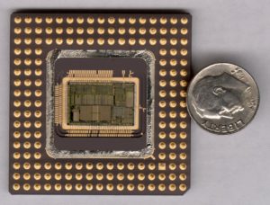
Reverse Engineering MCU ATmega1284V by unlock microcontroller ATmega1284V protective system, and readout heximal from microprocessor program memory, rewrite to the firmware to new ATmega1284V;
Reverse Engineering MCU ATmega1284V by unlock microcontroller ATmega1284V protective system, and readout heximal from microprocessor program memory, rewrite to the firmware to new ATmega1284V
The 8-bit comparator continuously compares TCNT0 with the Output Compare Registers (OCR0A and OCR0B). Whenever TCNT0 equals OCR0A or OCR0B, the comparator signals a match. A match will set the Output Compare Flag (OCF0A or OCF0B) at the next timer clock cycle. If the corresponding interrupt is enabled, the Output Compare Flag generates an Output Compare interrupt if attacking PIC16F506 MCU code.
The Output Compare Flag is automatically cleared when the interrupt is executed. Alternatively, the flag can be cleared by software by writing a logical one to its I/O bit location. The Waveform Generator uses the match signal to generate an output according to operating mode set by the WGM02:0 bits and Compare Output mode (COM0x1:0) bits after copy microcontroller PIC16F747 code.
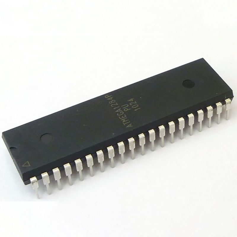
unlock ATMEGA1284P secured mcu fuse bit and extract embedded flash heximal file and eeprom binary program
The max and bottom signals are used by the Waveform Generator for handling the special cases of the extreme values in some modes of operation (“Modes of Operation” on page 121). Figure 40 shows a block diagram of the Output Compare unit. The OCR0x Registers are double buffered when using any of the Pulse Width Modulation (PWM) modes.
For the normal and Clear Timer on Compare (CTC) modes of operation, the double buffering is disabled. The double buffering synchronizes the update of the OCR0x Compare Registers to either top or bottom of the counting sequence.
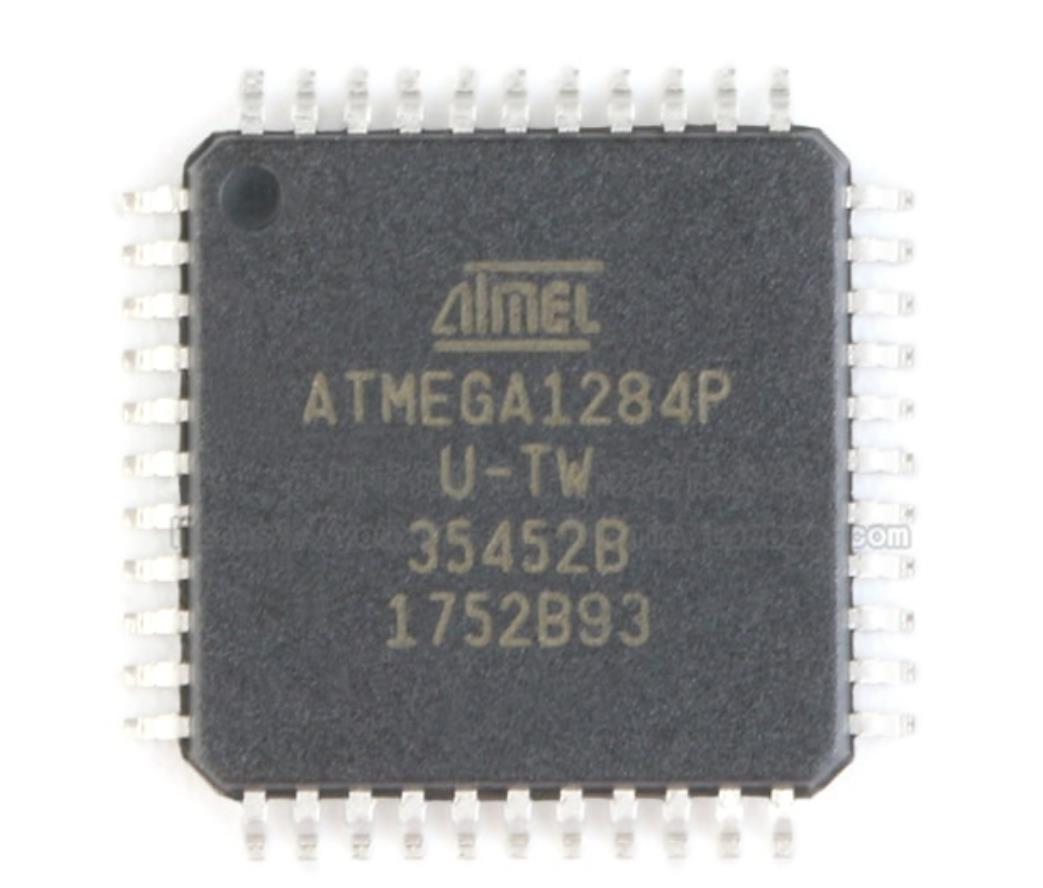
decrypt protected ATMEGA1284P controller and readout its flash firmware
The synchronization prevents the occurrence of odd-length, non-symmetrical PWM pulses, thereby making the output glitch-free. The OCR0x Register access may seem complex, but this is not case. When the double buffering is enabled, the CPU has access to the OCR0x Buffer Register, and if double buffering is disabled the CPU will access the OCR0x directly.