 Recover MCU ATtiny48 Heximal
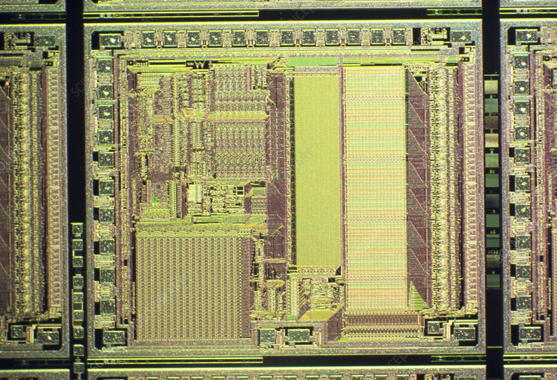
Recover MCU ATtiny48 Heximal from embedded flash and eeprom memory, unlock microcontroller attiny48 tamper resistance system and then copy the firmware from original attiny48 to the new MCU units;
During interrupts and subroutine calls, the return address Program Counter (PC) is stored on the Stack. The Stack is effectively allocated in the general data SRAM, and consequently the Stack size is only limited by the total SRAM size and the usage of the SRAM when Recover chip pic16c77 code.
All user programs must initialize the SP in the Reset routine (before subroutines or interrupts are executed). The Stack Pointer (SP) is read/write accessible in the I/O space. The data SRAM can easily be accessed through the five different addressing modes supported in the AVR architecture.
The memory spaces in the AVR architecture are all linear and regular memory maps. A flexible interrupt module has its control registers in the I/O space with an additional Global Interrupt Enable bit in the Status Register. All interrupts have a separate Interrupt Vector in the Interrupt Vector table when break pic16f636 Mcu.
The interrupts have priority in accordance with their Interrupt Vector position. The lower the Interrupt Vector address, the higher the priority. The I/O memory space contains 64 addresses for CPU peripheral functions as Control Registers, SPI, and other I/O functions.
The I/O Memory can be accessed directly, or as the Data Space locations following those of the Register File, 0x20 – 0x5F. In addition, the ATtiny48 has Extended I/O space from 0x60 – 0x1FF in SRAM where only the ST/STS/STD and LD/LDS/LDD instructions can be used after copy microcontroller pic16f767 program.
The high-performance AVR ALU operates in direct connection with all the 32 general purpose working registers. Within a single clock cycle, arithmetic operations between general purpose registers or between a register and an immediate are executed.
The ALU operations are divided into three main categories – arithmetic, logical, and bit-functions. Some implementations of the architecture also provide a powerful multiplier supporting both signed/unsigned multiplication and fractional format. See the “Instruction Set” section for a detailed description.
The Status Register contains information about the result of the most recently executed arithmetic instruction. This information can be used for altering program flow in order to perform conditional operations. Note that the Status Register is updated after all ALU operations, as specified in the Instruction Set Reference.
This will in many cases remove the need for using the dedicated compare instructions, resulting in faster and more compact code. The Status Register is not automatically stored when entering an interrupt routine and restored when returning from an interrupt. This must be handled by software.