Archive for August, 2012
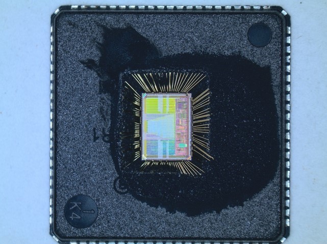
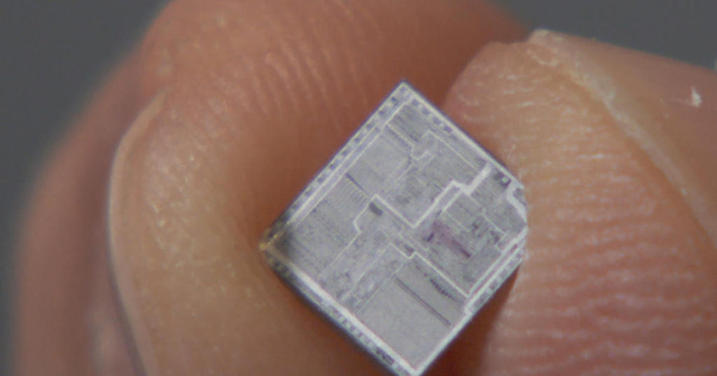
 Break Encrypted IC PIC16F76 Eeprom
Break Encrypted IC PIC16F76 Eeprom and flash memory, extract code from MCU PIC16F76 and copy firmware to new Microcontroller which will provide the same functions as original master processor;
Each PIC12C5XX instruction is a 12-bit word divided into an OPEEPROM, which specifies the instruction type, and one or more operands which further specify the operation of the instruction.
The PIC12C5XX instruction set summary in Table 9-2 groups the instructions into byte-oriented, bit-oriented, and literal and control operations. Table 9-1 shows the opeeprom field descriptions if recover pic16c505 encrypted Eeprom.
For byte-oriented instructions, ’f’ represents a file register designator and ’d’ represents a destination designator. The file register designator is used to specify which one of the 32 file registers is to be used by the instruction.
The destination designator specifies where the result of the operation is to be placed. If ’d’ is ’0’, the result is placed in the W register. If ’d’ is ’1’, the result is placed in the file register specified in the instruction.
Byte-oriented file register operations
For bit-oriented instructions, ’b’ represents a bit field designator which selects the number of the bit affected by the operation, while ’f’ represents the number of the file in which the bit is located when clone microcontroller pic16c54 heximal.
For literal and control operations, ’k’ represents an 8 or 9-bit constant or literal value.
All instructions are executed within a single instruction cycle, unless a conditional test is true or the program counter is changed as a result of an instruction.
In this case, the execution takes two instruction cycles. One instruction cycle consists of four oscillator periods. Thus, for an oscillator frequency of 4 MHz, the normal instruction execution time is 1 µs.
If a conditional test is true or the program counter is changed as a result of an instruction, the instruction execution time is 2 µs. Figure 9-1 shows the three general formats that the instructions can have. All examples in the figure use the following format to represent a hexadecimal number.
Further Improvement in Copy IC Code
Copy IC Code Further Improvement involved using a part of the main memory to control access to the data from outside. This was implemented either by latching the information stored at a certain address at power-up and treating it as a security fuse, or by using passwords to grant access to the memory.
For example, in the Texas Instruments MSP430F112 microcontroller, the read-back operation can be called only after the correct 32-bytes password is entered. Without that, only the chip erase operation is available. Although such protection seems to be more effective than previous offerings, it has some drawbacks which could be exploited in low-cost non-invasive mcu cracking such as timing microcontroller program reading and power analysis.
More details on these mcu flash recovery are presented in later articles. If the state of the security fuse is sampled from the memory during power-up or reset, it could present some room for the ic code copier to play with power glitches, trying to force the circuit to get the wrong state of the memory.
Recovery Chip PIC18F2480 Eeprom
Recovery Chip PIC18F2480 Eeprom content and copy firmware to new microcontroller PIC18F2480 by reset the security fuse bit of MCU through MCU cracking technique;
This family of devices offers the advantages of all PIC18 chips – namely, high computational performance at an economical price – with the addition of high-endurance, Enhanced Flash eeprom memory.
In addition to these features, the PIC18F2480/2580/4480/4580 family introduces design enhancements that make these chips a logical choice for many high-performance, power-sensitive applications if Reverse mcu atmega461pv binary.
All of the devices in the PIC18F2480/2580/4480/4580 family incorporate a range of features that can significantly reduce power consumption during operation.
Key items include:
Alternate Run Modes: By clocking the controller from the Timer1 source or the internal oscillator block, power consumption during code execution can be reduced by as much as 90% after break ic flash atmega461v flash.
Multiple Idle Modes: The controller can also run with its CPU core disabled but the peripherals still active. In these states, power consumption can be reduced even further, to as little as 4% of normal operation requirements.
On-the-Fly Mode Switching: The power-managed modes are invoked by user code during operation, allowing the user to incorporate power-saving ideas into their application’s software design.
Lower Consumption in Key Modules: The power requirements for both Timer1 and the Watchdog Timer have been reduced by up to 80%, with typical values of 1.1 and 2.1 ìA, respectively before Reverse ic atmega162p eeprom.
Extended Instruction Set: In addition to the standard 75 instructions of the PIC18 instruction set, PIC18F2480/2580/4480/4580 devices also provide an optional extension to the core CPU functionality. The added features include eight additional instructions that augment indirect and indexed addressing operations and the implementation of Indexed Literal Offset Addressing mode for many of the standard PIC18 instructions.
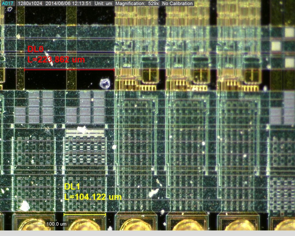
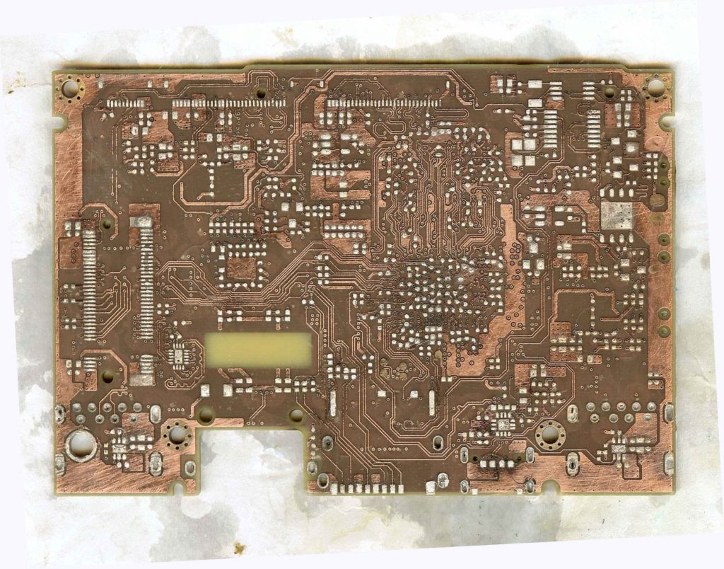
PCB Reproduce Background and Legitimacy Dispute
PCB Reproduce is way to manufacture printed circuit board through circuit diagram extraction method which include PCB board gerber file, layout, schematic diagram, the reproduced circuit board will provide the same functions as originals;
Background of PCB Reproduce technology can trace from the eighties of last century, Western developed countries are all committed to develop science and technology, and during which a variety of high-end technology electronic product being invented and widely applied.
Inventors of these products possess the whole set of technology solution and monopolize it from other competitior as well as society, some of these enterprises even deliberately increase the price of these products to attain higher profit. Under this circumstance, some competitors intend to break this monopolization and pursuit the rational profit from it and set out to reproduce these products through Printed circuit board schematic diagram restoration technology, consequently start to engage in the reproduce research of high tech product, that is what we so call PCB Reverse Engineering today.
Circuit Board reproduction is belong to the scope of reverse engineering technology, from the birthday of this concept, it is always being viewed as one of the most controversial subjects, PCB card cloning technology is playing an extremely important role in the integrated circuit industry, almost every countries in this world are applying this technology to get better knowledge of their competitor products, if this kind of action being strictly prohibited will only damage the development of integrated circuit industry.
Break Locked Chip PIC16F74 Data
Break Locked Chip PIC16F74 program memory and readout MCU Data from eeprom memory, the heximal file can be rewritten to the new microcontroller PIC16F74 for IC cloning;
If the data protection bit has not been programmed, the on-chip program memory can be read out for verification process. The first 64 locations can be read by the PIC16F74 regardless of the data protection bit setting.
The last memory location cannot be read if data protection is enabled on the PIC16F74. The last memory location can be read regardless of the data protection bit setting on the PIC16F74 if recover microprocessor atmega1281pa flash.
Four memory locations are designated as ID locations where the user can store checksum or other data-identification numbers. These locations are not accessible during normal execution but are readable and writable during program/verify.
Use only the lower 4 bits of the ID locations and always program the upper 8 bits as ’0’s. The PIC16F74 locked chips with EPROM program memory can be serially programmed while in the end application circuit before Break ic atmega2560pa heximal.
This is simply done with two lines for clock and data, and three other lines for power, ground, and the programming voltage. This allows customers to manufacture boards with unprogrammed devices, and then program the locked chip just before shipping the product.
This also allows the most recent firmware or a custom firmware to be programmed. The device is placed into a program/verify mode by holding the GP1 and GP0 pins low while raising the MCLR (VPP) pin from VIL to VIHH (see programming specification).
GP1 becomes the programming clock and GP0 becomes the programming data. Both GP1 and GP0 are Schmitt Trigger inputs in this mode if Break mcu atmega2560l flash.
After reset, a 6-bit command is then supplied to the device. Depending on the command, 14-bits of program data are then supplied to or from the device, depending if the command was a load or a read. For complete details of serial programming, please refer to the PIC12C5XX Programming Specifications. A typical in-circuit serial programming connection is shown in Figure 8-16.
Break MCU PIC16LF73 Heximal
Break MCU PIC16LF73 security fuse bit and extract program from microcontroller PIC16LF73 memory, clone Heximal file to processor;
A device may be powered down (SLEEP) and later powered up (Wake-up from SLEEP). The Power-Down mode is entered by executing a SLEEP instruction.
If enabled, the Watchdog Timer will be cleared but keeps running, the TO bit (STATUS<4>) is set, the PD bit (STATUS<3>) is cleared and the oscillator driver is turned off if recover microprocessor atmega1280pa flash heximal.
The I/O ports maintain the status they had before the SLEEP instruction was executed (driving high, driving low, or hi-impedance). It should be noted that a RESET generated by a WDT time-out does not drive the MCLR pin low.
For lowest current consumption while powered down, the T0CKI input should be at VDD or VSS and the GP3/MCLR/VPP pin must be at a logic high level (VIHMC) if MCLR is enabled after Break reverse engineering MCU atmega48pv code.
The device can wake-up from SLEEP through one of the following events:
An external reset input on GP3/MCLR/VPP pin, when configured as MCLR. A Watchdog Timer time-out reset (if WDT was enabled). A change on input pin GP0, GP1, or GP3/MCLR/VPP when wake-up on change is enabled.
These events cause a device reset. The TO, PD, and GPWUF bits can be used to determine the cause of device reset. The TO bit is cleared if a WDT time-out occurred (and caused wake-up).
The PD bit, which is set on power-up, is cleared when SLEEP is invoked. The GPWUF bit indicates a change in state while in SLEEP at pins GP0, GP1, or GP3 (since the last time there was a file or bit operation on GP port) before recover MCU atmega88pv firmware.
Caution: Right before entering SLEEP, read the input pins. When in SLEEP, wake up occurs when the values at the pins change from the state they were in at the last reading. If a wake-up on change occurs and the pins are not read before reentering SLEEP, a wake up will occur immediately even if no pins change while in SLEEP mode. The WDT is cleared when the device wakes from sleep, regardless of the wake-up source.
PCB Reengineering
PCB Reengineering is one of the related concept of PCB Reverse Engineering, it means to relayout or remodify the PCB Gerber File extracted from PCB Clone process for the purpose of functionality modification of original PCB Board which can provide a fast path to realize the product upgrade to satisfy the customized and personalized requirement from individual customer.
Hack IC Code through Security Fuse
Hack IC Code through Security Fuse is a method suits for a part of microcontroller unlocking such as ATmel and Microchip MCUs, the security fuse bit normally embed in the memory;
The next step was to make the security fuse part of the memory access circuit, so that any external access to the data is disabled if the fuse is set. Usually the fuse is located very close to the main MCU memory or evhen shares some control lines with it. Also it is fabricated with the same technology as the main MCU memory array making it harder to locate and reset.
Non-invasive IC firmware hacking could still exist but would require much time and effort to find. At the same time, semi-invasive MCU crack might still work. Certainly it would take more time for engineer to find the security fuse or the part of the control circuit responsible for the security monitoring, but this could be easily automated. Performing invasive IC code attack could be more difficult as most of the work would need to be done manually, so it will certainly increase the cost and time to extract IC code.
Decrypt Locked MCU PIC16LF72 Heximal
Decrypt Locked MCU PIC16LF72 and readout microcontroller PIC16LF72 Heximal from program memory and eeprom memory, normally the protection of MCU will be unlocked;
The WDT has a nominal time-out period of 18 ms, (with no prescaler). If a longer time-out period is desired, a prescaler with a division ratio of up to 1:128 can be assigned to the WDT (under software control) by writing to the OPTION register.
Thus, a time-out period of a nominal 2.3 seconds can be realized. These periods vary with temperature, VDD and part-to- part process variations (see DC specs) if break IC ATmega1284 firmware.
Under worst case conditions (VDD = Min., Temperature = Max., max. WDT prescaler), it may take several seconds before a WDT time-out occurs.
The CLRWDT instruction clears the WDT and the postscaler, if assigned to the WDT, and prevents it from timing out and generating a device RESET.
The SLEEP instruction resets the WDT and the postscaler, if assigned to the WDT. This gives the maximum SLEEP time before a WDT wake-up reset when reverse engineering mcu atmega1284pv firmware.
The TO, PD, and GPWUF bits in the STATUS register can be tested to determine if a RESET condition has been caused by a power-up condition, a MCLR or Watchdog Timer (WDT) reset.
A brown-out is a condition where device power (VDD) dips below its minimum value, but not to zero, and then recovers. The device should be reset in the event of a brown-out.
To reset PIC12C5XX devices when a brown-out occurs, external brown-out protection circuits may be built, This circuit will activate reset when VDD goes below Vz + 0.7V (where Vz = Zener voltage).* Refer to Figure 8-7 and Table 11-1 for internal weak pull-up on MCLR. This brown-out protection circuit employs Microchip Technology’s MCP809 microcontroller supervisor. The MCP8XX and MCP1XX family of supervisors provide push-pull and open collector outputs with both high and low active reset pins. There are 7 different trip point selections to accomodate 5V and 3V systems.
Add Security Fuse to Prevent IC Code Attack
Add Security Fuse to Prevent IC Code Attack is commonly used way to extract embedded firmware from MCU flash and eeprom memory;
The next step in increasing the security protection against IC code attack which was in adding a hardware security fuse that disables the access to data.
The easiest implementation, which does not require the complete redesign of the microcontroller structure, was for the fuse to control the read-back function of the programming interface.
The drawback of this approach was in making it easier to locate the security fuse and perform an invasive MCU breaking. For example, the state of the fuse could be changed by connecting the output from the fuse cell directly to the power supply or ground line.
In some cases it might be enough to just disconnect the sense circuit from the fuse cell by cutting the wire from it with a laser cutter or focused ion beam (FIB) machine.
It might be possible to succeed in non-invasive mcu code extraction as well, because a separate fuse would certainly behave differently from the normal memory array. As a result it might be possible to find such a combination of external signals under which the state of this fuse would not be read correctly thus allowing the access to the information stored in the on-chip memory.
Semi-invasive MCU cracking could bring the code reading to success even faster but will require decapsulation of the chip to get access to the die. A well known example of such attacks is erasing the security fuse under a UV light.