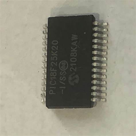
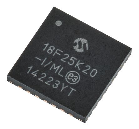
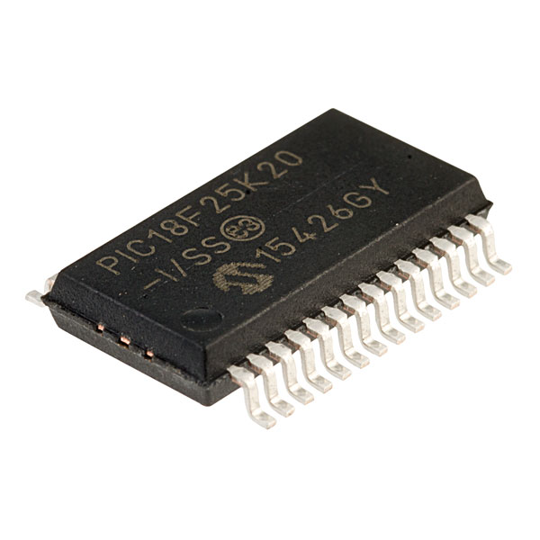
 Revese Microcontroller PIC18F25K20 Locked Heximal
Revese Microcontroller PIC18F25K20 Locked Heximal is a way to crack mcu pic18f25k20 fuse bit and extract embedded code from flash memory;
While the program memory can be addressed in only one way – through the program counter – information in the data memory space can be addressed in several ways. For most instructions, the addressing mode is fixed. Other instructions may use up to three modes, depending on which operands are used and whether or not the extended instruction set is enabled.
The addressing modes are:
- Inherent
- Literal
- Direct
- Indirect
- Literal
An additional addressing mode, Indexed Literal Offset, is available when the extended instruction set is enabled (XINST Configuration bit = 1). Its operation is discussed in greater detail in Section 5.5.1 “Indexed Addressing with Literal Offset”.
Защищенный микроконтроллер Revese Engineering PIC18F25K20 заблокированным шестнадцатеричным файлом или двоичными данными – это способ взлома защитного микроконтроллера PIC18F25K20 бита предохранителя и извлечения исходного кода встроенной прошивки из зашифрованного микропроцессора PIC18F25K20 флэш-памяти и памяти EEPROM;
Many PIC18 control instructions do not need any argu- ment at all; they either perform an operation that glob- ally affects the device or they operate implicitly on one register. This addressing mode is known as Inherent Addressing.
Examples include SLEEP, RESET and DAW. Other instructions work in a similar way but require an additional explicit argument in the opcode when breaking microchip mcu pic18f14k50 flash memory. This is known as Literal Addressing mode because they require some literal value as an argument. Examples include ADDLW and MOVLW, which respectively, add or move a literal value to the W register. Other examples include CALL and GOTO, which include a 20-bit program memory address.
revese engenharia microcontrolador seguro PIC18F25K20 bloqueado arquivo heximal ou dados binários é uma maneira de quebrar MCU protetor PIC18F25K20 fusível bit e extrair o código-fonte de firmware incorporado do microprocessador criptografado PIC18F25K20 memória flash e memória eeprom;
Direct addressing specifies all or part of the source and/or destination address of the operation within the opcode itself. The options are specified by the arguments accompanying the instruction. In the core PIC18 instruction set, bit-oriented and byte-oriented instructions use some version of direct addressing by default which can faciliate the process of pic18f23k20 memory unit attacking.
revese مهندسی میکروکنترلر امن PIC18F25K20 فایل هگزیمال قفل شده و یا داده های باینری یک راه برای کرک محافظ MCU PIC18F25K20 فیوز بیت و استخراج کد منبع سیستم عامل تعبیه شده از ریزپردازنده رمزگذاری شده PIC18F25K20 حافظه فلش و حافظه eeprom است؛
All of these instructions include some 8-bit literal address as their Least Significant Byte. This address specifies either a register address in one of the banks of data RAM (Section 5.3.3 “GeneralPurpose Register File”) or a location in the Access Bank (Section 5.3.2 “Access Bank”) as the data source for the instruction.