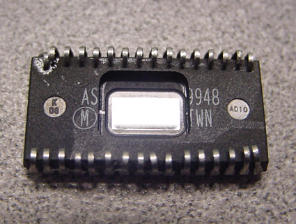
Reverse Engineering Chip ATmega640PV Locked Flash
We can reverse engineering chip ATMEGA640PV locked flash, please view the chip ATMEGA640PV features for your reference:
In ATmega640PV four Port B pins – PB2, PB3, PB4, and PB5 – have alternative functions as inputs for the ADC. If some Port B pins are configured as outputs, it is essential that these do not switch when a conversion is in progress.
This might corrupt the result of the conversion. During Power-down mode and ADC Noise Reduction mode, the Schmitt triggers of the digital inputs are disconnected on these pins if reverse engineering chip locked flash.
This allows an analog input voltage close to VCC/2 to be present during Power-down without causing excessive power consumption. The Port B pins with alternate functions are shown in Table 1 on page 4.
When the pins PB4..0 are used for the alternate function, the DDRB and PORTB registers have to be set according to the alternate function description. When PB5 is used as external reset pin, the values in the corresponding DDRB and PORTB bit are ignored after Reverse Engineering Chip ATmega640PV Locked Flash.
The Port B Input Pins address (PINB) is not a register, and this address enables access to the physical value on each Port B pin. When reading PORTB, the PORTB Data Latch is read, and when reading PINB, the logical values present on the pins are read.
The lower five pins in Port B are equal when used as digital I/O pins. PBn, general I/O pin: The DDBn bit in the DDRB register selects the direction of this pin if Reverse Engineering Chip ATmega640PV Locked Flash.
If DDBn is set (one), PBn is configured as an output pin. If DDBn is cleared (zero), PBn is configured as an input pin. If PORTBn is set (one) when the pin is configured as an input pin, the MOS pull-up resistor is activated.
To switch the pull-up resistor off, the PORTBn has to be cleared (zero) or the pin has to be configured as an output pin. Pull-ups for all ports can be disabled also by setting PUD-bit in the MCUCR register.
Timing Attack Application
Timing attacks can be applied to microcontrollers whose security protection is based on passwords, or to access control systems that use cards or keys with fixed serial numbers, for example, Dallas iButton products. The common mistake in such systems is the way the serial number of the entered key is verified against the database. Very often the system checks each byte of the key against one entry in the database and stops as soon as an incorrect byte is found. Then it switches to the next entry in the database until it reaches the end. So the attacker can easily measure the time between the input of the last key and the request for another key and figure out how many coincidences were found. With a relatively small number of attempts, he will be able to find one of the matching keys.
Break IC ATmega640A Secured Flash
We can break IC ATMEGA640A secured flash, please view the IC ATMEGA640A features for your reference:
If differential channels are selected, the differential gain stage amplifies the voltage difference between the selected input pair by the selected gain factor, 1x or 20x, according to the setting of the MUX2..0 bits in ADMUX..
This amplified value then becomes the analog input to the ADC. If single-ended channels are used, the gain amplifier is bypassed altogether.
If ADC2 is selected as both the positive and negative input to the differential gain amplifier (ADC2 – ADC2), the remaining offset in the gain stage and conversion circuitry can be measured directly as the result of the conversion before Break IC ATmega640A Secured Flash.
This figure can be subtracted from subsequent conversions with the same gain setting to reduce offset error to below 1 LSB. The ADC can operate in two modes – Single Conversion and Free Running after break IC secured flash.
In Single Conversion mode, each conversion will have to be initiated by the user. In Free Running mode, the ADC is constantly sampling and updating the ADC Data Register. The ADFR bit in ADCSR selects between the two available modes when Break IC ATmega640A Secured Flash.
The ADC is enabled by setting the ADC Enable bit, ADEN in ADCSR. Voltage reference and input channel selections will not go into effect until ADEN is set. The ADC does not consume power when ADEN is cleared, so it is recommended to switch off the ADC before entering Power-saving sleep modes if break IC secured flash.
A conversion is started by writing a logical “1” to the ADC Start Conversion bit, ADSC. This bit stays high as long as the conversion is in progress and will be set to zero by hardware when the conversion is completed.
If a different data channel is selected while a conversion is in progress, the ADC will finish the current conversion before performing the channel change.
The ADC generates a 10-bit result, which is presented in the ADC data registers, ADCH and ADCL. By default, the result is presented right-adjusted, but can optionally be presented left-adjusted by setting the ADLAR bit in ADMUX after BREAK IC.
Prevent Timing IC Attack
To prevent Timing IC attack the techniques used for blinding signatures can be used. The general idea is to prevent the attacker knowing the input to the modular exponentiation operation by mixing the input with a chosen random value.
Decrypt Locked Microcontroller PIC24FJ16GA002 Software
We can decrypt locked Microcontroller PIC24FJ16GA002 software, please view the locked Microcontroller PIC24FJ16GA002 features for your reference:
If the result is left-adjusted and no more than 8-bit precision is required, it is sufficient to read ADCH. Otherwise, ADCL must be read first, then ADCH, to ensure that the content of the data registers belongs to the same conversion.
Once ADCL is read, ADC access to data registers is blocked. This means that if ADCL has been read, and a conversion completes before ADCH is read, neither register is updated and the result from the conversion is lost.
When ADCH is read, ADC access to the ADCH and ADCL registers is re-enabled. The ADC has its own interrupt, which can be triggered when a conversion completes before decrypt locked Microcontroller PIC24FJ16GA002 software.
When ADC access to the data registers is prohibited between reading of ADCH and ADCL, the interrupt will trigger even if the result is lost. The successive approximation circuitry requires an input clock frequency between 50 kHz and 200 kHz.
Using a higher input frequency will affect the conversion accuracy, see “ADC Characteristics” on page 50. The ADC module contains a prescaler, which divides the system clock to an acceptable ADC clock frequency.
The ADPSn bits in ADCSR are used to generate a proper ADC clock input frequency from any CK frequency above 100 kHz. The prescaler starts counting from the moment the ADC is switched on by setting the ADEN bit in ADCSR if decrypt locked Microcontroller PIC24FJ16GA002 software.
The prescaler keeps running for as long as the ADEN bit is set, and is continuously reset when ADEN is low. When initiating a conversion by setting the ADSC bit in ADCSR, the conversion starts at the following rising edge of the ADC clock cycle.
If differential channels are selected, the conversion will only start at every other rising edge of the ADC clock cycle after ADEN was set after RECOVER MCU.
Necessary information before timing attack
To conduct the attack one needs to collect a set of messages, together with their processing time, e.g. question-answer delay. Many cryptographic algorithms were found to be vulnerable to timing attacks. The main reason why this happens is in the software implementation of each algorithm. That includes performance optimisation to bypass unnecessary branching and conditional operations, cache memory usage, non-fixed time processor instructions such as multiplication and division, and a wide variety of other causes. As a result performance characteristics typically depend on both the encryption key and the input data.
Break Secured MCU ATmega88PA Program
We can break secured mcu ATMEGA88PA program, please view the secured mcu ATMEGA88PA features for your reference:
When writing serial data to the ATtiny15L, data is clocked on the rising edge of SCK. When reading data from the ATtiny15L, data is clocked on the falling edge of SCK. See Figure 34, Figure 35, and Table 28 for timing details.
To program and verify the ATtiny15L in the Serial Programming mode, the following sequence is recommended (See 4-byte instruction formats in Table 27):
Power-up sequence:
Apply power between VCC and GND while RESET and SCK are set to “0 ”. If the programmer cannot guarantee that SCK is held low during Power-up, RESET must be given a positive pulse of at least two MCU cycles duration after SCK has been set to “0” if Break Secured MCU ATmega88PA Program.
Wait for at least 20 ms and enable serial programming by sending the Programming Enable serial instruction to the MOSI (PB0) pin. Refer to the above section for minimum low and high periods for the serial clock input SCK.
The serial programming instructions will not work if the communication is out of synchronization. When in sync, the second byte ($53) will echo back when issuing the third byte of the Programming Enable instruction.
Whether the echo is correct or not, all four bytes of the instruction must be transmitted. If the $53 did not echo back, give SCK a positive pulse and issue a new Programming Enable instruction. If the $53 is not seen within 32 attempts, there is no functional device connected when Break Secured MCU ATmega88PA Program.
If a Chip Erase is performed (must be done to erase the Flash), wait tWD_ERASE after the instruction, give RESET a positive pulse, and start over from step 2. See Table 29 on page 63 for tWD_ERASE value.
The Flash or program array is programmed one byte at a time by supplying the address and data together with the appropriate write instruction. An program memory location is first automatically erased before new data is written. Use data polling to detect when the next byte in the Flash or program can be written before Break Secured MCU ATmega88PA Program.
If polling is not used, wait tWD_PROG_FL or tWD_PROG_EE, respectively, before transmitting the next instruction. See Table 30 on page 63 for the tWD_PROG_FL and tWD_PROG_EE values. In an erased device, no $FFs in the data file(s) need to be programmed after BREAK IC.
Any memory location can be verified by using the Read instruction, which returns the content at the selected address at the serial output MISO (PB1) pin.
At the end of the programming session, RESET can be set high to commence normal operation.
Power-off sequence (if needed):
Set RESET to “1”.
Turn VCC power off.
Recover The System Secret Key
Some security-related operations a semiconductor chip performs can take a different time to compete depending on the values of the input data and the secret key. Careful timing measurement and analysis may allow recovery of the system’s secret key. This idea was first published in the scientific literature in 1996. Then later these attacks were successfully performed on an actual smartcard implementation of the RSA signature.
Restricting access to information on memory programming
Another simple trick many semiconductor manufacturers use is restricting access to information on memory programming. This is normally used for smartcards, but on some microcontrollers such information is not publicly available as well. This is not a reliable and practical way of making the design secure. Of course it works well with smartcards where all the customers are obliged to sign a non-disclosure agreement with the chip manufacturer. But microcontrollers, with very few exceptions, can be programmed with universal programmers that are widely available from different companies around the world. Even if the programming specification is not documented, all the necessary waveforms can be easily extracted in a few hours with using any low cost oscilloscope, because all the signals are normally applied with less than 1 MHz frequency. If the microcontroller is not supported by a particular universal programmer, it is always possible to buy the development kit directly from the manufacturer and obtain all the necessary protocols from it directly.
Reverse Engineering IC ATmega88PV Locked Flash
We can reverse engineering IC ATMEGA88PV locked flash, please view the IC ATMEGA88PV features for your reference:
When a byte is being programmed into the Flash or EEPROM, reading the address location being programmed will give the value $FF. At the time the device is ready for a new byte, the programmed value will read correctly.
This is used to determine when the next byte can be written.
This will not work for the value $FF so when programming this value, the user will have to wait for at least tWD_PROG_FL before programming the next Flash byte, or tWD_PROG_EE before the next EEPROM byte if Reverse Engineering IC ATMEGA88PV Locked Flash.
As a chip-erased device contains $FF in all locations, programming of addresses that are meant to contain $FF can be skipped. This does not apply if the EEPROM is reprogrammed without chip-erasing the device.
In that case, data polling cannot be used for the value $FF and the user will have to wait at least tWD_PROG_EE before programming the next byte. See Table 30 for tWD_PROG_FL and tWD_PROG_EE values.
Stresses beyond those listed under “Absolute Maximum Ratings” may cause permanent damage to the device. This is a stress rating only and functional operation of the device at these or other conditions beyond those indicated in the operational sections of this specification is not implied when Reverse Engineering IC ATMEGA88PV Locked Flash.
Exposure to absolute maximum rating conditions for extended periods may affect device reliability.
Note:
“Max” means the highest value where the pin is guaranteed to be read as low if reverse engineering IC locked flash.
“Min” means the lowest value where the pin is guaranteed to be read as high.
Although each I/O port can sink more than the test conditions (20 mA at VCC = 5V, 10 mA at VCC = 3V) under steady state conditions (non-transient), the following must be observed before reverse engineering IC locked flash:
1] The sum of all IOL, for all ports, should not exceed 100 mA. If IOL exceeds the test condition, VOL may exceed the related specification. Pins are not guaranteed to sink current greater than the listed test conditions.
Although each I/O port can source more than the test conditions (3 mA at VCC = 5V, 1.5 mA at VCC = 3V) under steady state conditions (non-transient), the following must be observed when reverse engineering IC locked flash:
1] The sum of all IOH, for all ports, should not exceed 100 mA. If IOH exceeds the test condition, VOH may exceed the related specification. Pins are not guaranteed to source current greater than the listed test condition if Reverse Engineering IC ATMEGA88PV Locked Flash.