 Unlock ARM Microcontroller STM32F070RCT6 Secured Flash Memory
 January 12th, 2021 |
  Author:
 The STM32F070RCT6 is a versatile ARM microcontroller widely adopted in modern embedded electronic products that demand reliable processing, efficient power consumption, and compact integration. Based on the ARM Cortex architecture, this MCU is commonly found in industrial automation systems, smart instrumentation, consumer electronics, energy management devices, communication equipment, and advanced control platforms. One of its strengths is the integration of internal flash memory and peripheral resources that allow manufacturers to store operational firmware, application program logic, configuration data, and system parameters directly inside the device. To preserve intellectual property and protect product integrity, these resources are often configured as protected, locked, secured, or encrypted, making long-term maintenance and migration increasingly difficult once original development resources become unavailable.
External interrupt/event controller (EXTI)
The external interrupt/event controller consists of 23 edge-detector lines used to generate interrupt/event requests. Each line can be independently configured to select the trigger event (rising edge, falling edge, both) and can be masked independently. A pending register maintains the status of the interrupt requests. The EXTI can detect an external line with a pulse width shorter than the Internal APB2 clock period. Up to 140 GPIOs can be connected to the 16 external interrupt lines.
Hizmetimiz; erişilebilir ikili verilerin, hexadecimal dosyaların ve yapılandırma verilerinin yapılandırılmış biçimde çıkarılması ve yeniden oluşturulmasını destekler; böylece erişilemeyen ARM STM32F070RCT6 MCU içeriği düzenli mühendislik kaynaklarına dönüştürülür.
Gelişmiş laboratuvar analizleri ve kontrollü yarı iletken değerlendirme yöntemleri aracılığıyla, uygun yetkilendirme bulunduğu durumlarda ARM STM32F070RCT6 mikrodenetleyicisinin gömülü bellek koruma çalışmaları, mimari çözümleme ve geçmişe ait flash ile EEPROM içeriklerinin geri kazanımını içeren projeleri destekliyoruz.
Ürün sürekliliği gerektiren müşteriler için, geri kazanılmış ARM STM32F070RCT6 mikroişlemci firmware’leri uyumluluk analizini, kontrollü kopya doğrulamasını ve uzun vadeli ürün destek planlamasını destekleyebilir.
Clocks and startup
On reset the 16 MHz internal RC oscillator is selected as the default CPU clock. The 16 MHz internal RC oscillator is factory-trimmed to offer 1% accuracy. The application can then select as system clock either the RC oscillator or an external 4-26 MHz clock source. This clock is monitored for failure. If failure is detected, the system automatically switches back to the internal RC oscillator and a software interrupt is generated (if enable). Similarly, full interrupt management of the PLL clock entry is available when necessary (for example if an indirectly used external oscillator fails). The advanced clock controller clocks the core and all peripherals using a single crystal or oscillator. In particular, the ethernet and USB OTG FS peripherals can be clocked by the system clock.
Nasza usługa wspiera uporządkowaną ekstrakcję i rekonstrukcję dostępnych danych binarnych, plików szesnastkowych i danych konfiguracyjnych, przekształcając niedostępną zawartość MCU ARM STM32F070RCT6 w uporządkowane zasoby inżynieryjne.
Dzięki zaawansowanym analizom laboratoryjnym i kontrolowanym metodom oceny półprzewodników wspieramy projekty związane z zachowaniem pamięci wbudowanej, analizą architektury oraz odzyskiwaniem historycznych zawartości pamięci Flash i EEPROM mikrokontrolera ARM STM32F070RCT6, tam gdzie istnieją odpowiednie uprawnienia.
Dla klientów wymagających ciągłości produktu odzyskane firmware mikroprocesora ARM STM32F070RCT6 mogą wspierać analizę kompatybilności, kontrolowaną walidację duplikacji oraz długoterminowe planowanie wsparcia produktu.
Our “Unlock ARM Microcontroller STM32F070RCT6 Secured Flash Memory” service focuses on helping customers regain access to their own valuable engineering assets through lawful recovery, preservation, and analysis workflows. Rather than replacing proven hardware platforms, organizations often seek to retrieve historical firmware archives, preserve operational program files, and recover critical source code references that support maintenance and lifecycle extension. Our service supports structured extraction and reconstruction of available binary, heximal, and configuration data, transforming inaccessible device content into organized engineering resources. Through advanced laboratory analysis and controlled semiconductor evaluation methods, we support projects involving embedded memory preservation, architecture decode, and recovery of historical flash and EEPROM contents where appropriate authorization exists. For customers requiring product continuity, recovered assets may support compatibility analysis, controlled duplicate validation, and long-term product support planning.
Наша послуга підтримує структуроване вилучення та реконструкцію доступних бінарних, шістнадцяткових і конфігураційних даних, перетворюючи недоступний вміст MCU ARM STM32F070RCT6 на впорядковані інженерні ресурси.
Завдяки передовому лабораторному аналізу та контрольованим методам дослідження напівпровідників ми підтримуємо проєкти зі збереження вбудованої пам’яті, декодування архітектури та відновлення історичного вмісту Flash і EEPROM мікроконтролера ARM STM32F070RCT6 за наявності відповідного дозволу.
Для клієнтів, яким необхідна безперервність продукту, відновлені прошивки мікропроцесора ARM STM32F070RCT6 можуть підтримувати аналіз сумісності, контрольовану перевірку дублювання та довгострокове планування підтримки продукту.
From a technical perspective, our methodology emphasizes analysis, validation, and preservation rather than destructive experimentation. Depending on device condition and project scope, workflows may include physical inspection, controlled package evaluation, and non-invasive assessment techniques designed to understand internal storage organization. In selected cases, specialized laboratory procedures may be used to examine device structures and assist with data retrieval and archive reconstruction. Extracted binary files are organized and interpreted to recover meaningful firmware structures, helping reconstruct historical program behavior and supporting engineering documentation. Where customers require continuity planning, recovered information can assist with system modernization, controlled clone verification, configuration comparison, and migration of legacy embedded environments while maintaining operational consistency.
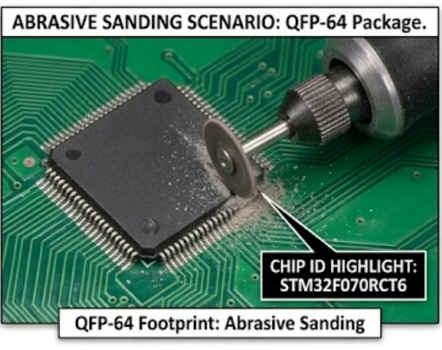
Naše služba podporuje strukturovanou extrakci a rekonstrukci dostupných binárních, hexadecimálních a konfiguračních dat a převádí nepřístupný obsah MCU ARM STM32F070RCT6 na organizované technické zdroje.
Pomocí pokročilé laboratorní analýzy a řízených metod hodnocení polovodičů podporujeme projekty zaměřené na uchování vestavěné paměti, dekódování architektury a obnovu historického obsahu pamětí Flash a EEPROM mikrokontroléru ARM STM32F070RCT6 tam, kde existuje odpovídající oprávnění.
Pro zákazníky vyžadující kontinuitu produktů mohou obnovené firmwary mikroprocesoru ARM STM32F070RCT6 podpořit analýzu kompatibility, řízené ověřování duplikace a dlouhodobé plánování podpory produktů.
For end users, recovering information from STM32F070RCT6 secured flash memory can create significant long-term value. Manufacturers can preserve legacy platforms, reduce redevelopment effort, maintain compatibility across product generations, and improve support for installed systems. Access to historical firmware, archived data, and structured memory records allows engineering teams to document existing products and extend service life without unnecessary redesign. By combining deep experience in ARM architectures with disciplined recovery and decode processes, our service provides a dependable pathway for preserving critical technical assets and maintaining continuity across complex embedded systems.
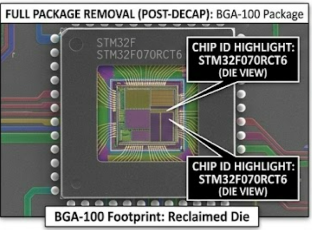
Нашата услуга поддържа структурирано извличане и реконструкция на налични бинарни, шестнадесетични и конфигурационни данни, като преобразува недостъпното съдържание на ARM STM32F070RCT6 MCU в организирани инженерни ресурси.
Чрез усъвършенстван лабораторен анализ и контролирани методи за оценка на полупроводници подпомагаме проекти, свързани със съхраняване на вградена памет, декодиране на архитектура и възстановяване на историческо съдържание от Flash и EEPROM паметта на микроконтролера ARM STM32F070RCT6, когато съществува съответното разрешение.
За клиенти, които изискват непрекъснатост на продукта, възстановените фърмуери на микропроцесора ARM STM32F070RCT6 могат да подпомогнат анализ на съвместимостта, контролирано валидиране на дублиране и дългосрочно планиране на продуктовата поддръжка.
 Posted in
Microprocessor ST72F324BJ Program Flash Memory Unlocking
Microprocessor ST72F324BJ Program Flash Memory Unlocking will take the advantage of focus ion beam to remove the fuse bit embedded and pull embedded firmware out from mcu st72f324bj memory, after a few moment later these extracted heximal can be copied to new st72f324bj for micrcontroller cloning;
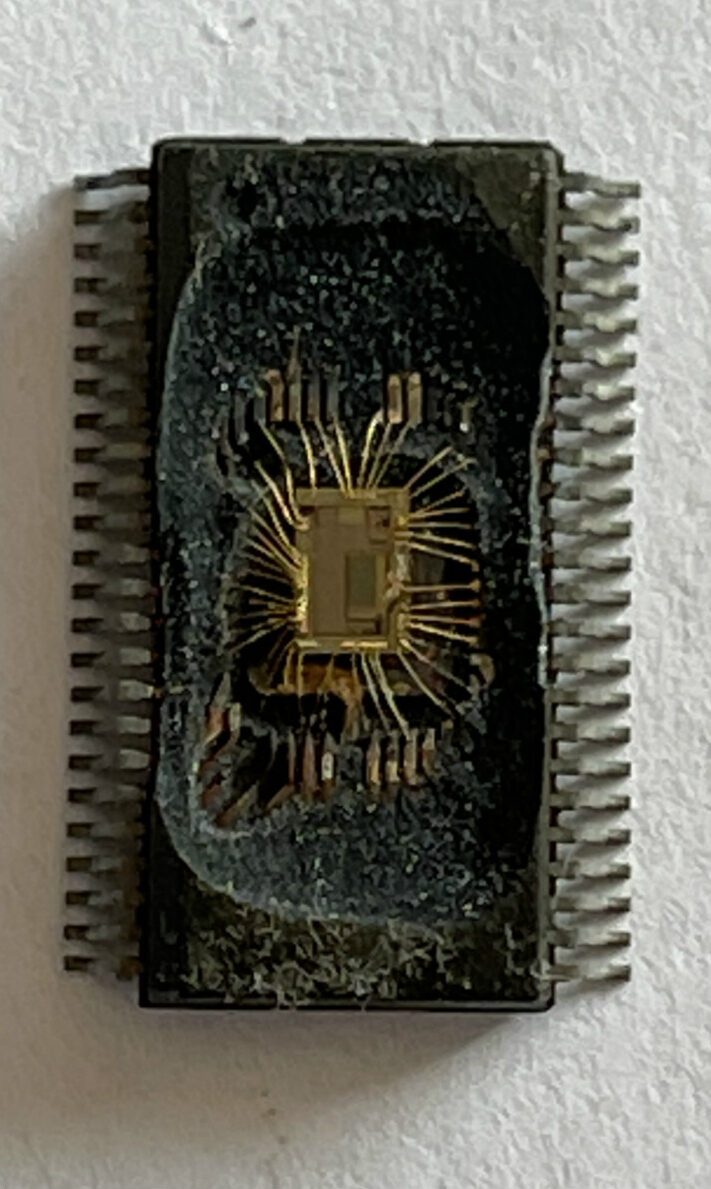
The ST7 dual voltage High Density Flash (HDFlash) is a non-volatile memory that can be electrically erased as a single block or by individu- al sectors and programmed on a Byte-by-Byte ba- sis using an external VPP supply.
The HDFlash devices can be programmed and erased off-board (plugged in a programming tool) or on-board using ICP (In-Circuit Programming) or IAP (In-Application Programming). The array matrix organisation allows each sector to be erased and reprogrammed without affecting other sectors.
Read-out protection, when selected, provides a protection against Program Memory content ex- traction and against write access to Flash memo- ry. Even if no protection can be considered as to- tally unbreakable, the feature provides a very high level of protection for a general purpose microcon- troller.
In flash devices, this protection is removed by re- programming the option. In this case, the entire program memory is first automatically erased and the device can be reprogrammed.
Read-out protection selection depends on the de- vice type:
- In Flash devices it is enabled and removed through the FMP_R bit in the option byte.
In ROM devices it is enabled by mask option specified in the Option List.
Crack ST72F321M9 Secured Microcontroller
Crack ST72F321M9 Secured Microcontroller and pull the embedded firmware from st72f321m9 locked flash memory, copy heximal file into new microprocessor st72f321m9 memory;
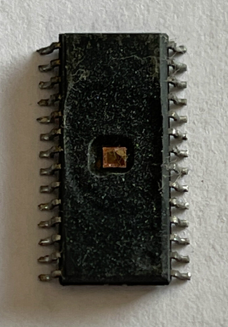
the MCU is capable of addressing 64K bytes of memories and I/O registers. The available memory locations consist of 128 bytes of register locations, up to 2Kbytes of RAM and up to 60Kbytes of user program memory when st72f321bk mcu flash memory program decryption. The RAM space includes up to 256 bytes for the stack from 0100h to 01FFh.
The highest address bytes contain the user reset and interrupt vectors.
IMPORTANT: Memory locations marked as “Re- served” must never be accessed. Accessing a re- seved area can have unpredictable effects on the device.
Related Documentation
AN 985: Executing Code in ST7 RAM
The ST7 dual voltage High Density Flash (HDFlash) is a non-volatile memory that can be electrically erased as a single block or by individu- al sectors and programmed on a Byte-by-Byte ba- sis using an external VPP supply.
The HDFlash devices can be programmed and erased off-board (plugged in a programming tool) or on-board using ICP (In-Circuit Programming) or IAP (In-Application Programming) even in the process of decoding mcu st72f321r9 locked memory file. The array matrix organisation allows each sector to be erased and reprogrammed without affecting other sectors.
Extract Microcontroller ST72F321BAR9T6 Flash Memory Source Code
Extract Microcontroller ST72F321BAR9T6 Flash Memory Source Code needs to use focus ion beam to remove its security fuse bit which will refers to pull embedded firmware from st72f321ba flash memory, and then copy flash firmware in the format of heximal to new st72f321ba mcu chip;
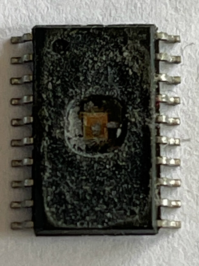
The ST7 dual voltage High Density Flash (HDFlash) is a non-volatile memory that can be electrically erased as a single block or by individu- al sectors and programmed on a Byte-by-Byte ba- sis using an external VPP supply.
The HDFlash devices can be programmed and erased off-board (plugged in a programming tool) or on-board using ICP (In-Circuit Programming) or IAP (In-Application Programming). The array matrix organisation allows each sector to be erased and reprogrammed without affecting other sectors when breaking st72f321ar ic chip memory protection.
Three Flash programming modes:
Insertion in a programming tool. In this mode, all sectors including option bytes can be pro- grammed or erased.
ICP (In-Circuit Programming). In this mode, all sectors including option bytes can be pro- grammed or erased without removing the de- vice from the application board.
IAP (In-Application Programming) In this mode, all sectors except Sector 0, can be pro- grammed or erased without removing the device from the application board and while the application is running in the process of st72f321bk microprocessor flash memory program decryption.
ICT (In-Circuit Testing) for downloading and executing user application test patterns in RAM
Read-out protection
Register Access Security System (RASS) to prevent accidental programming or erasing
Encrypted MCU STM8L052R8 Flash Heximal Decoding
The stm8l052r8 is a low-power mcu from stmicro, designed for embedded applications where efficient energy consumption, dependable control, and compact integration are important. This microcontroller can be found in smart instruments, industrial monitoring equipment, metering systems, battery-powered devices, consumer electronics, sensor controllers, access systems, and other products requiring reliable embedded control. Its integrated storage resources allow application firmware, configuration data, calibration parameters, and program information to remain inside the device.
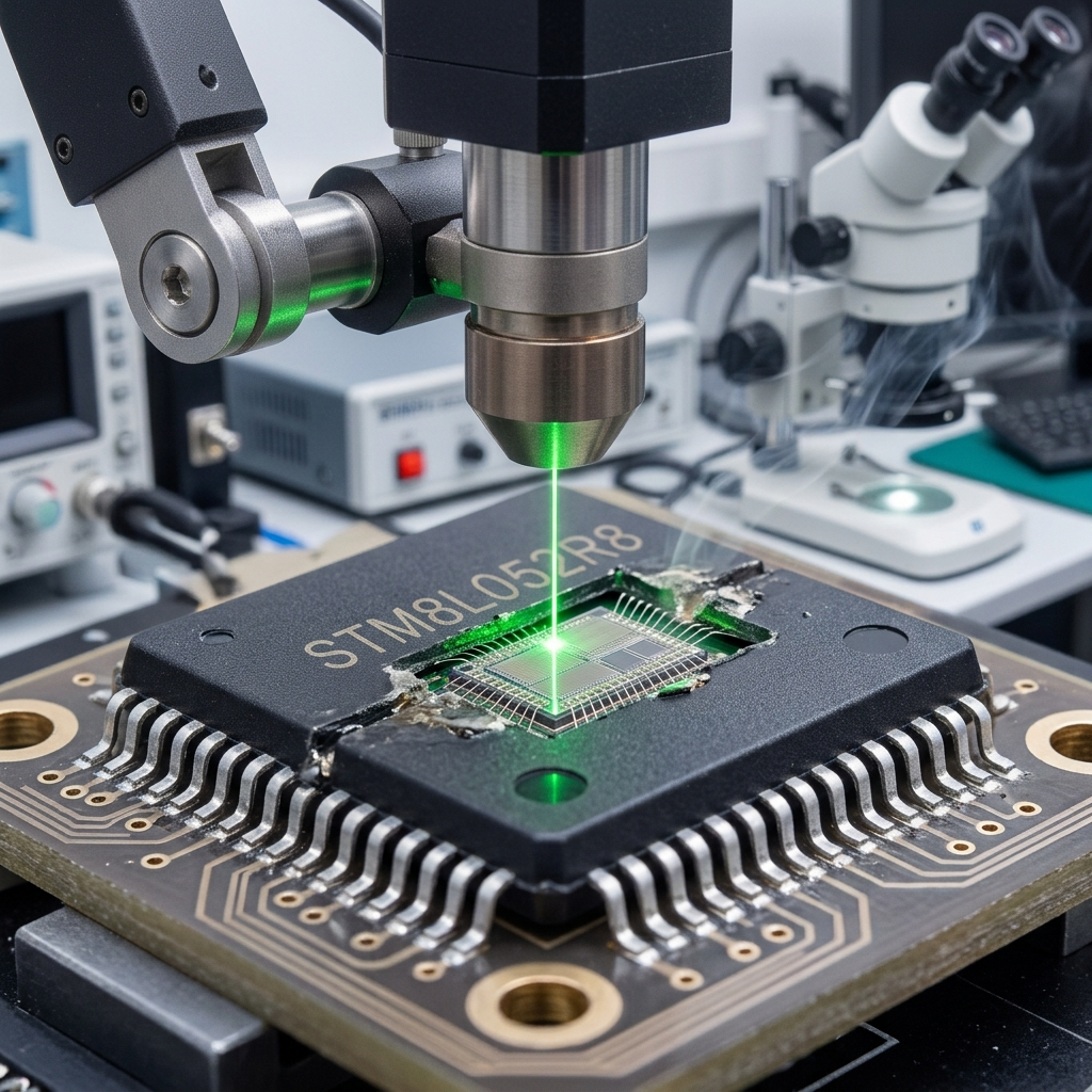
For engineering teams supporting long-life products, these resources can become extremely valuable when original development projects are no longer available. A manufacturer may have the physical product but lack its original source code, binary, heximal, or engineering archive. Furthermore, firmware may be stored in protected, locked, secured, or encrypted form. Our “encrypted mcu stm8l052r8 flash heximal decoding” service addresses these situations through professional analysis, recovery, and preservation of authorized embedded software assets.
The device has an integrated ZEROPOWER power-on reset (POR)/power-down reset (PDR). For the device sales types without the “D” option (see Section 11: Ordering information), it is coupled with a brownout reset (BOR) circuitry. It that case the device operates between 1.8 and 3.6 V, BOR is always active and ensures proper operation starting from 1.8 V.
Our engineers begin by evaluating the target stm8l052r8, its physical condition, surrounding circuitry, and available technical documentation. The objective is to determine what flash, eeprom, and memory information can be recovered and how that information relates to the original embedded application. Depending on the device condition and project authorization, advanced laboratory investigation may be considered, including carefully controlled decapsulate analysis where conventional examination cannot provide sufficient information. Available firmware, binary, and heximal records can then be examined and decoded into structured engineering data, file, and archive resources.

When customers describe the requirement as encrypted flash decryption, attack, break, or hack, our professional approach remains focused on authorized recovery rather than supplying instructions for defeating security protections. Recovery feasibility depends on the specific architecture and protection implementation, so every protected, locked, or encrypted device requires individual assessment. Where technically feasible, recovered information can be used to retrieve historical program resources, support controlled clone evaluation, duplicate development, compatibility testing, maintenance, or reconstruction of missing engineering documentation.
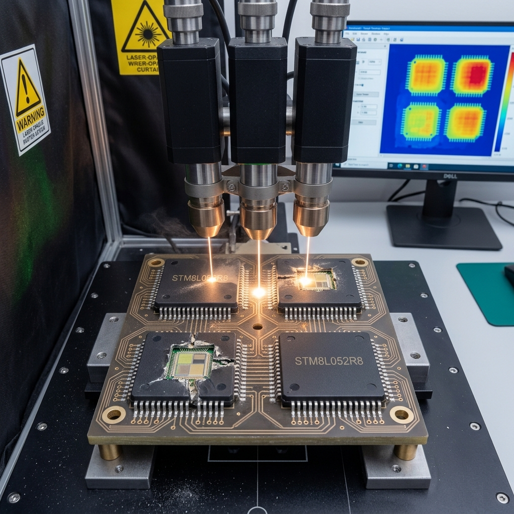
After the 1.8 V BOR threshold is reached, the option byte loading process starts, either to confirm or modify default thresholds, or to disable BOR permanently (in which case, the VDD min. value at power-down is 1.65 V) in order to recover embedded data ee-prom content from stm8s005k6 microcontroller.
Five BOR thresholds are available through option bytes, starting from 1.8 V to 3 V. To reduce the power consumption in Halt mode, it is possible to automatically switch off the internal reference voltage (and consequently the BOR) in Halt mode as the consequence of stm8s207s8 microprocessor reverse engineering. The device remains in reset state when VDD is below a specified threshold, VPOR/PDR or VBOR, without the need for any external reset circuit.
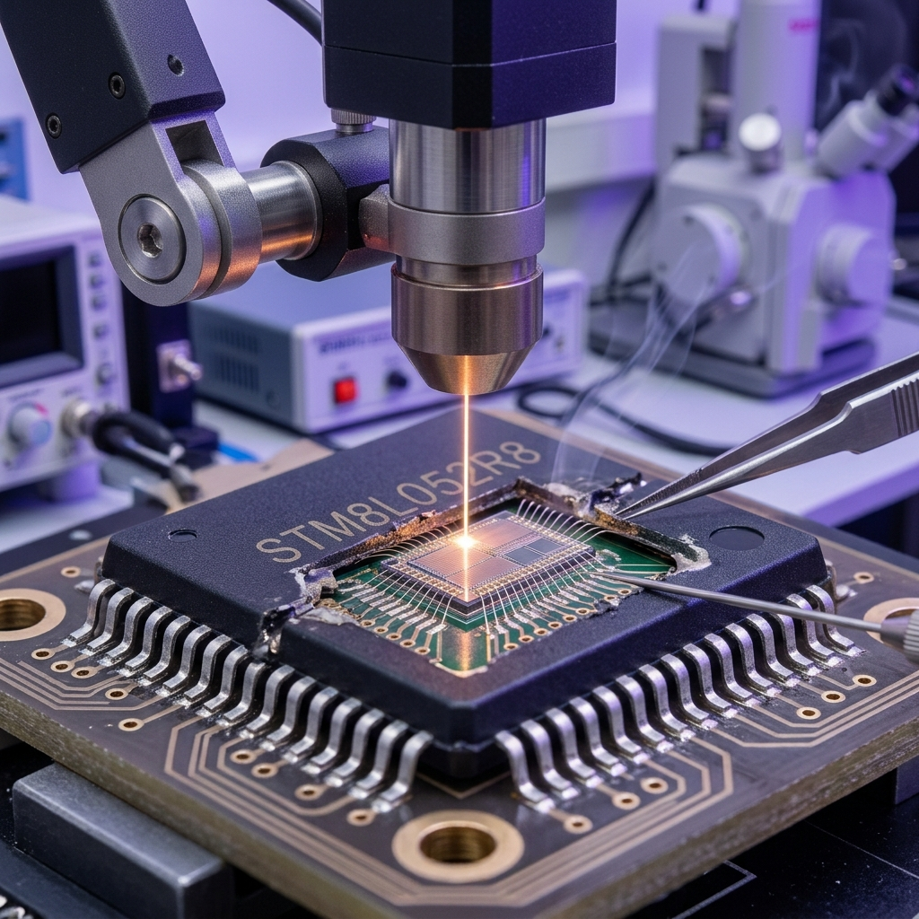
An important part of heximal decoding is recognizing that a recovered image does not necessarily contain the original developer source code. Compiled firmware generally consists of machine-readable instructions and data structures, requiring additional engineering interpretation before its function can be understood. Our specialists can correlate available binary information with PCB connections, peripheral behavior, communication interfaces, timing characteristics, and system responses to establish a clearer picture of the embedded application.
The microprocessor architecture, memory organization, configuration parameters, and firmware behavior are considered together rather than analyzed independently. Where appropriate, semiconductor-level decapsulate investigation can complement software analysis and provide additional technical evidence. The resulting engineering package may include validated firmware information, organized heximal or binary files, memory observations, program documentation, and technical archive materials that can serve as references for future development.
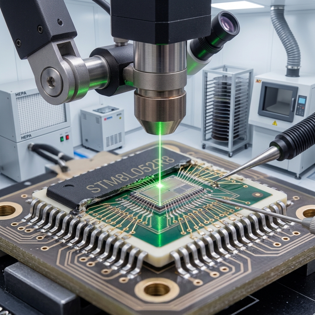
For manufacturers, repair organizations, and authorized engineering teams, recovering stm8l052r8 firmware can provide meaningful lifecycle advantages. Historical firmware, data, and program resources can reduce redevelopment work, support obsolete equipment, improve troubleshooting, and provide a foundation for hardware modernization. Companies may use recovered engineering information to develop replacement boards, migrate established functions to newer devices, document legacy products, or preserve valuable intellectual property.
Rather than abandoning a mature product because its original software environment has disappeared, an organization can investigate the existing mcu and determine which embedded resources remain available. By combining stmicro device expertise, firmware analysis, memory investigation, and structured heximal decoding, our service helps transform inaccessible embedded information into practical engineering resources for maintenance, restoration, compatibility analysis, and long-term product continuity.
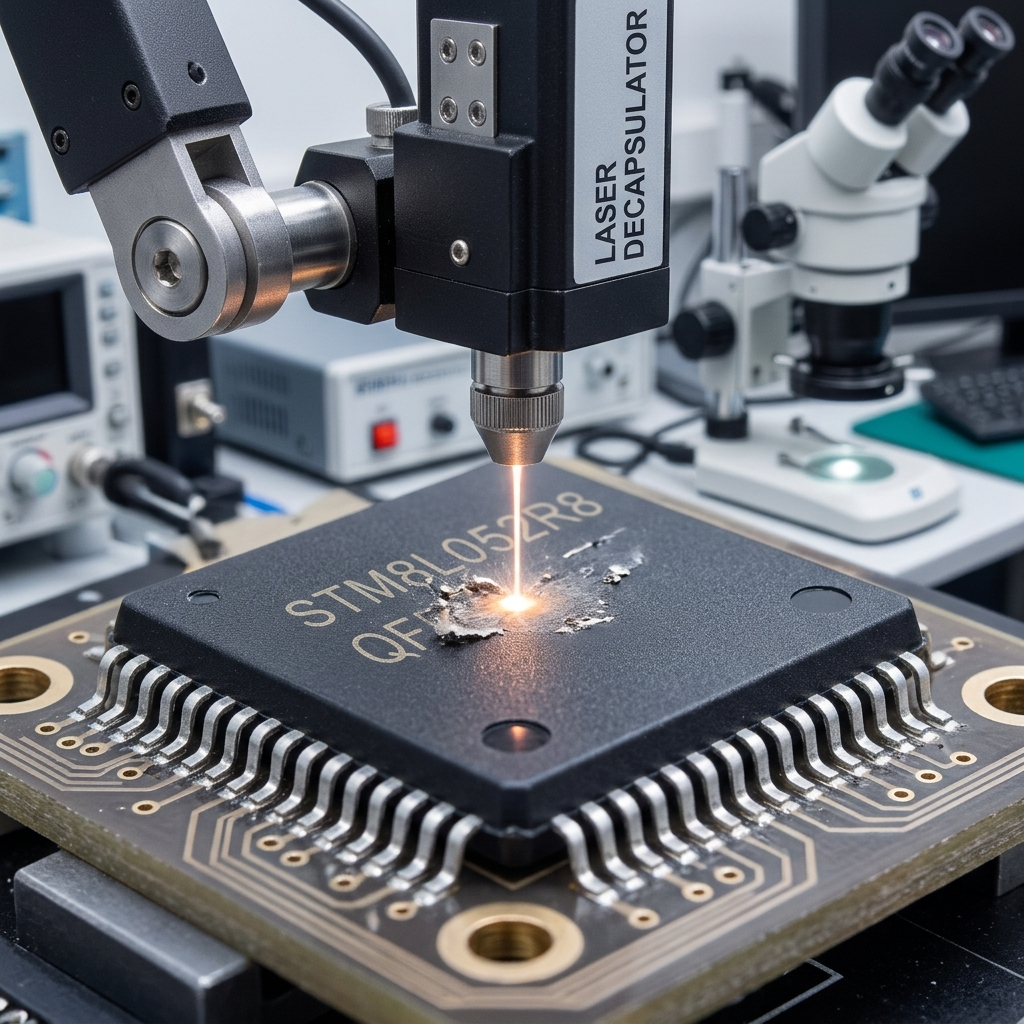
STMicrocontroller STM8L052C6T6 Locked Flash Memory Decryption
The stm8l052c6t6 is a compact low-power mcu from stmicro designed for embedded products where energy efficiency, reliable control, and long operating life are important. Its capabilities make this microcontroller suitable for applications including industrial monitoring, smart meters, battery-powered instruments, consumer electronics, access-control equipment, sensor nodes, portable measurement devices, and specialized control modules.
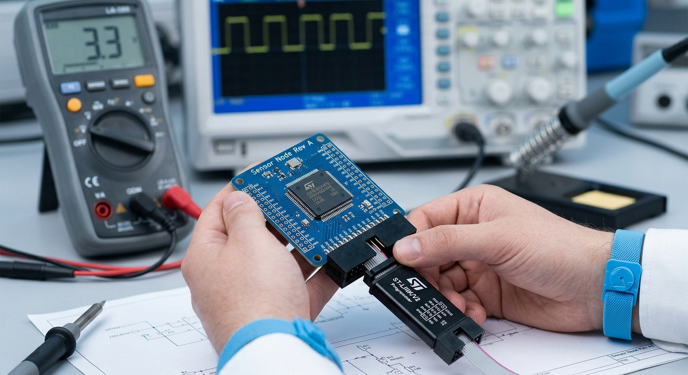
Within these products, the microprocessor can execute application logic while internal flash, eeprom, and memory resources preserve firmware, configuration data, calibration values, and program information. For manufacturers, this embedded information can represent years of engineering investment. However, original source code, development projects, binary, heximal, and engineering archive files may become unavailable as products age.
At the same time, internal storage can be configured as protected, locked, secured, or otherwise encrypted, creating a significant challenge when an organization needs to maintain an existing product. Our “stmicrocontroller stm8l052c6t6 locked flash memory decryption” service is designed to address authorized firmware preservation and engineering recovery requirements involving this type of embedded system.
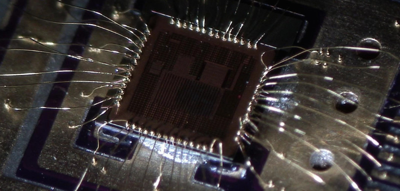
The high-density and medium+ density STM8L15xx6/8x devices feature a nested vectored interrupt controller:
Nested interrupts with 3 software priority levels
32 interrupt vectors with hardware priority
Up to 40 external interrupt sources on 11 vectors
Trap and reset interrupts
The device requires a 1.65 V to 3.6 V operating supply voltage (VDD). The external power supply pins must be connected as follows:
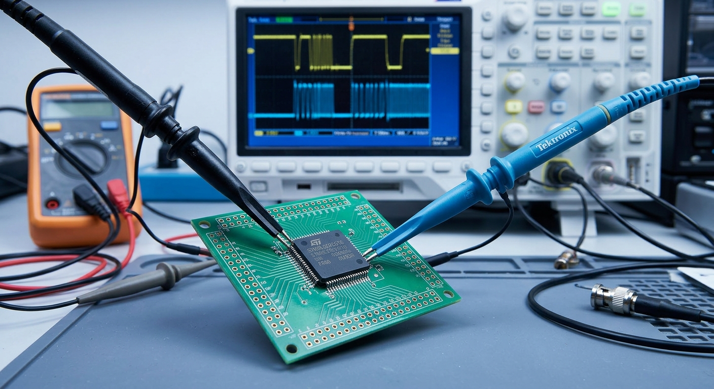
Our service begins with a detailed assessment of the target stm8l052c6t6, its circuit environment, physical condition, and available engineering documentation. Rather than assuming that every locked device can simply be attacked, breaken, or hacked, our engineers first determine the architecture and establish what information can realistically be recovered. Depending on the device and project requirements, controlled semiconductor investigation may be considered, including specialized decapsulate analysis where appropriate and authorized. Available flash, eeprom, and memory information can then be evaluated to determine whether useful firmware, binary, heximal, or configuration data remains accessible. Advanced analysis can retrieve relevant information and decode it into organized file and archive resources for engineering evaluation.
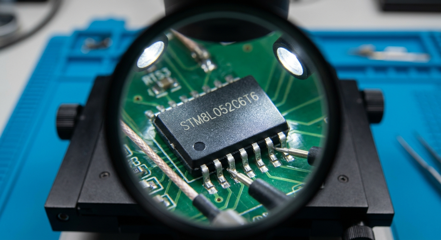
When the customer describes the requirement as locked flash memory decryption, the practical objective is to recover and interpret customer-owned embedded resources rather than provide unauthorized access techniques. Where technically feasible, recovered program information may support controlled clone evaluation, duplicate development, compatibility verification, product repair, or reconstruction of missing documentation. Each protected, locked, or secured device is assessed individually because recovery feasibility depends on the semiconductor architecture and implemented protection mechanism.
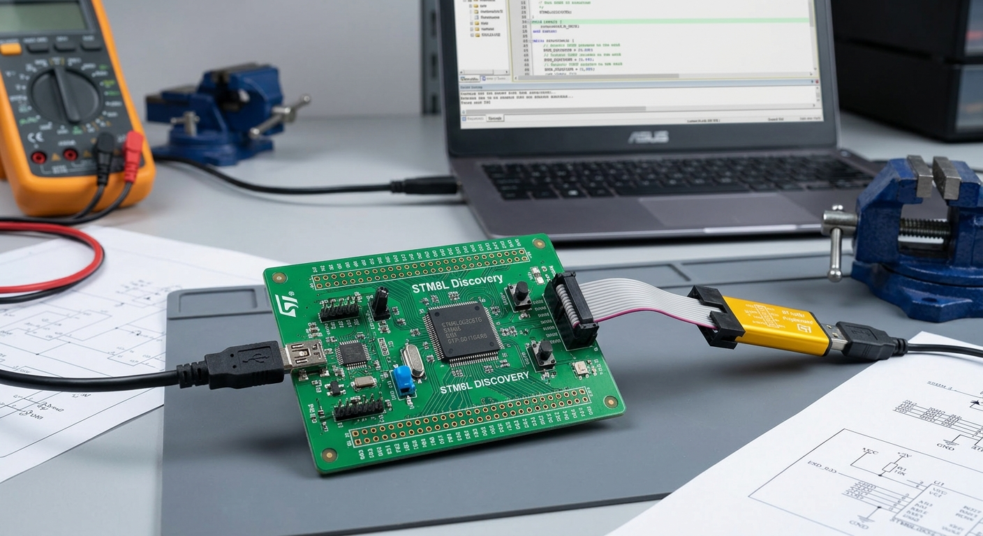
The engineering value of this process extends beyond obtaining a raw memory image. Compiled firmware normally consists of machine-level binary information rather than the developer’s original source code, so professional analysis is required to interpret its functional structure. Engineers can correlate recovered data with PCB connections, peripheral behavior, communication interfaces, timing characteristics, and other system functions to build a more complete understanding of the original product.
Where suitable, laboratory-level decapsulate investigation can complement conventional firmware analysis and help clarify inaccessible internal structures. The resulting technical package may include validated firmware information, organized binary or heximal files, memory observations, program documentation, and engineering archive records. This approach is particularly valuable when an obsolete product must remain operational but its original development environment, programmer configuration, or source files have disappeared.
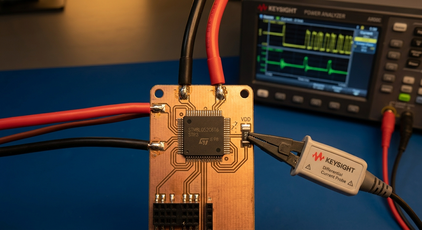
For equipment manufacturers, maintenance organizations, and authorized product owners, professional recovery of stm8l052c6t6 flash information can reduce redevelopment costs and extend the service life of established products. Recovered firmware, program, and data resources can assist with troubleshooting, replacement-board development, product migration, documentation reconstruction, and future modernization.
Instead of recreating a mature embedded system entirely from the beginning, engineering teams can use information recovered from an existing mcu as a technical reference for continued development. Our service combines embedded-system expertise, stmicro device analysis, memory investigation, and firmware reconstruction to help customers preserve valuable engineering knowledge contained within existing hardware and maintain continuity across long-life electronic products.
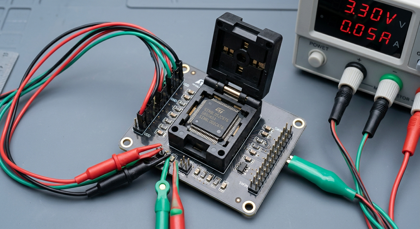
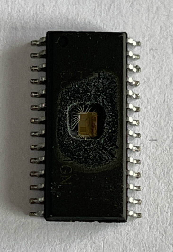
Duplicate DSP TMS320F28055PNT Microcontroller Binary
The TMS320F28055PNT is a digital signal controller from Texas Instruments’ C2000 family, designed for embedded systems that require fast real-time processing, accurate control, and integrated peripheral resources. As a DSP-oriented microcontroller, it is particularly suitable for applications where control algorithms, signal processing, feedback monitoring, and precise timing need to operate together within a dedicated electronic system.
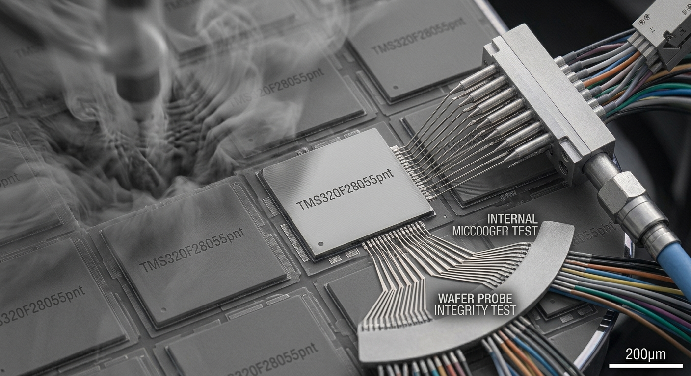
Its capabilities make it applicable to motor drives, industrial automation, digital power supplies, solar and renewable-energy equipment, inverters, power conversion systems, energy-management equipment, and other industrial control platforms. In these applications, the programmed controller can contain essential operating logic that determines how the equipment responds to sensors, power stages, motors, communications, and other hardware, making preservation of its binary information important when maintaining established products.
To designate the stages in the product development cycle, TI assigns prefixes to the part numbers of all TMS320™ MCU devices and support tools. Each TMS320 MCU commercial family member has one of three prefixes: TMX, TMP, or TMS (for example, TMS320F28069). Texas Instruments recommends two of three possible prefix designators for its support tools: TMDX and TMDS. These prefixes represent evolutionary stages of product development from engineering prototypes (with TMX for devices and TMDX for tools) to fully qualified production devices/tools (with TMS for devices and TMDS for tools).
Device development evolutionary flow:
When an electronic controller has been operating successfully for years, the original development environment may no longer be available even though the programmed TMS320F28055PNT remains functional. Missing source code, firmware projects, engineering documentation, software backups, or archived production files can create difficulties when a controller needs to be repaired or reproduced. A protective, secured, encrypted, or locked device can add another layer of difficulty by preventing conventional access to its internal program memory. For authorized equipment owners and engineers, recovering the available firmware or binary information can support replacement-board development, discontinued-product maintenance, controller duplication, troubleshooting, functional comparison, and long-term preservation. In particular, an accessible binary image can provide a valuable reference when the objective is to reproduce an existing controller without having to recreate the original embedded application entirely from the beginning.
TMP Final silicon die that conforms to the device’s electrical specifications but has not completed quality and reliability verification
TMS Fully qualified production device Support tool development evolutionary flow:
For a TMS32F28055PNT binary recovery project, engineers can first inspect the target hardware, identify the processor and its programming or debugging interfaces, and evaluate its memory organization and protection configuration. Depending on the device condition and authorized objective, technical methods can be investigated to determine whether firmware, source code, data, software, memory, archive, flash, or eeprom information can be retrieved, decoded, duplicated, or cloned.

If a protective, secured, encrypted, or locked configuration restricts normal readout, specialists may evaluate appropriate approaches to break or attack the relevant access restriction. Where conventional interface methods cannot provide sufficient information, advanced semiconductor analysis may include controlled decapsulation of the microcontroller, microprocessor, MCU, chip, or IC. The practical result depends on the specific protection condition, physical state, memory contents, available interfaces, and recovery requirements of the target TMS32F28055PNT; therefore, the feasibility of producing a usable binary from another TMS32F28055PNT must be assessed individually, while any work involving a third TMS32F28055PNT should likewise be based on its actual device condition rather than a universal recovery assumption.

Our TMS320F28055PNT binary duplication and firmware recovery service helps authorized manufacturers, equipment owners, repair companies, and engineering teams preserve important embedded software from existing control systems. We can examine the target board, identify the installed DSP controller, investigate available programming and debugging paths, and evaluate memory and protection conditions before selecting a suitable recovery strategy.
Where technically feasible, our service can assist with obtaining recoverable firmware or binary information and preparing it for authorized replacement-controller programming, product restoration, redesign, engineering analysis, or maintenance. This is particularly useful when the original source-code archive has disappeared but a working or partially functional controller remains available. By combining device identification, hardware investigation, memory analysis, firmware examination, and specialized recovery techniques, we help customers preserve valuable binary information and support the continued operation or reproduction of established electronic control equipment.

Reverse Engineering Texas Instrument TMS320F28054PNQ Flash Memory
The TMS320F28054PNQ is a digital signal controller in Texas Instruments’ C2000™ family, developed for demanding real-time control applications that require fast computation, precise timing, and integrated peripheral functions. Based on a control-oriented architecture, the device combines processing resources with memory and peripheral functions intended for applications such as motor control, digital power conversion, renewable-energy equipment, industrial automation, power supplies, inverters, and other embedded control systems.
Its integrated control resources allow engineers to implement functions such as waveform generation, feedback monitoring, communications, and real-time control algorithms within a dedicated electronic controller. For industrial equipment, the processor can therefore become a key component whose embedded Flash program determines important operating characteristics of the finished product.
The TI Reference Design Library is a robust reference design library spanning analog, embedded processor, and connectivity. Created by TI experts to help you jump start your system design, all reference designs include schematic or block diagrams, BOMs, and design files to speed your time to market. Search and download designs at the Select TI reference designs page.
Digitally Controlled Non-Isolated DC/DC Buck Converter Reference Design
This design implements a non-isolated DC/DC buck converter that is digitally controlled using a C2000 microcontroller. The main purpose of this design is to evaluate the powerSUITE Digital Power Software tools. The design consists of two separate boards: 1) Digital Power BoosterPack™ Plug-in Module and
2) C2000 F28069M LaunchPad™ Development Kit or C2000 F28377S LaunchPad Development Kit. 672W Highly Integrated Reference Design for Automotive Bidirectional 48V-12V Converter Today’s automotive power consumption is 3KW, which will increase to 10KW in the next 5 years. A 12-V battery is unable to provide that much power. The 48-12V bidirectional convertor provides a high-power requirement solution with two phases, each capable of running 28 A. This solution allows bidirectional current control of both phases using a C2000 control stick and firmware OCP and OVP. The 48-12V bidirectional converter removes the voltage conditioner need and distributes loads more evenly. The 48-V battery is used to power high-torque motors and other high-power components, such as A/C compressors and EPS, with no change to 12-V battery loads.
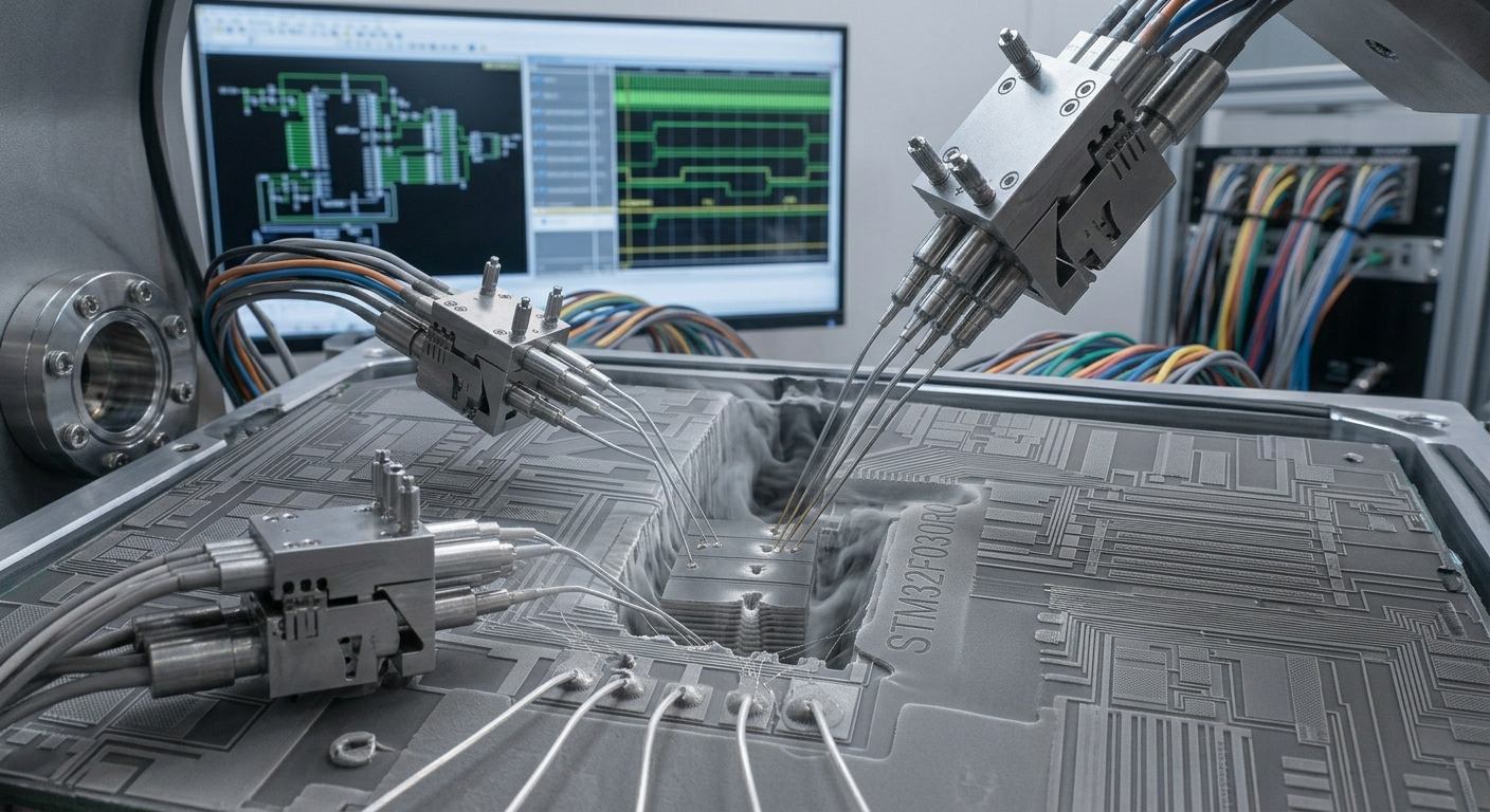
The disappearance of an original firmware project can become a serious issue when equipment has already entered long-term production or remains in service. source code, firmware backups, software archives, engineering files, and other development documentation may be unavailable after years of product maintenance, staff changes, or discontinued development environments. Meanwhile, the original TMS320F28054PNQ may still contain the program required to operate a functioning controller.
If its internal memory is protective, secured, encrypted, or locked, ordinary programming procedures may not provide the information required for repair or reproduction. Authorized Flash memory recovery can consequently help engineers investigate legacy equipment, restore damaged controllers, develop replacement boards, preserve discontinued designs, or analyze an existing implementation when the original software archive is no longer accessible.
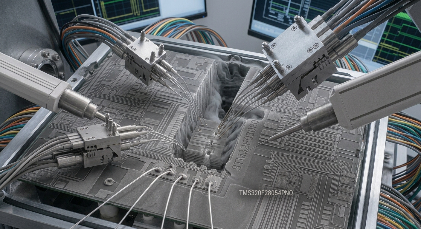
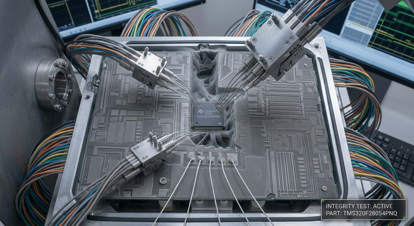
For a TMS32F28054 reverse-engineering project, the first stage can involve identifying the processor, examining the target circuit, checking available programming or debugging interfaces, and evaluating the memory and protection configuration. Depending on the device condition and authorized recovery objective, specialists can investigate whether firmware, source code, data, software, memory, archive, flash, or eeprom information can be retrieved, decoded, duplicated, or cloned. When a protective, secured, encrypted, or locked configuration restricts standard access, suitable technical approaches may be considered to break or attack the applicable access restriction.
If interface-based methods cannot provide sufficient information, advanced semiconductor analysis may involve controlled decapsulation and examination of the microcontroller, microprocessor, MCU, chip, or IC. The achievable result for each TMS32F28054 depends on its actual protection status, physical condition, memory architecture, interface accessibility, and the required recovery scope, while a complete or partial recovery for another TMS32F28054 should likewise be determined through individual technical assessment rather than assumed in advance.
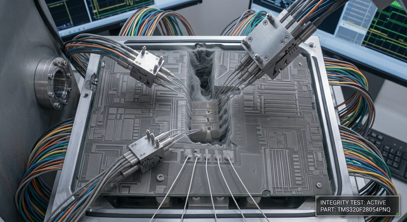
Our TMS320F28054PNQ Flash memory and firmware recovery service is designed to help authorized end users, equipment manufacturers, repair organizations, and engineering teams preserve valuable embedded software from existing electronic systems. We can inspect the target hardware, identify the processor and available interfaces, assess the memory and protection condition, and determine a technically appropriate recovery strategy. Where feasible, the service can assist with recovering usable firmware images, Flash contents, configuration information, or other embedded data for authorized repair, restoration, redesign, replacement-controller development, and engineering analysis.
This can be particularly important for industrial products whose original development files are no longer available but whose installed controllers continue to contain essential operating software. By combining hardware examination, memory analysis, firmware investigation, and specialized semiconductor recovery techniques, we help customers obtain valuable information from legacy control systems and support the continued maintenance of established electronic products.
Decode ST CPU ST72F321R9 Processor Locked Memory File
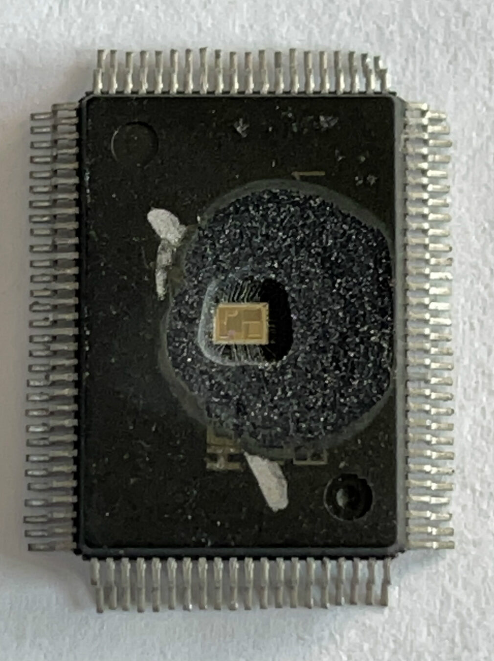
Decode ST CPU ST72F321R9 Processor Locked Memory File needs to use laser cutting to remove the security fuse bit of microcontroller, and then copy embedded flash firmware from mcu st72f321r9;
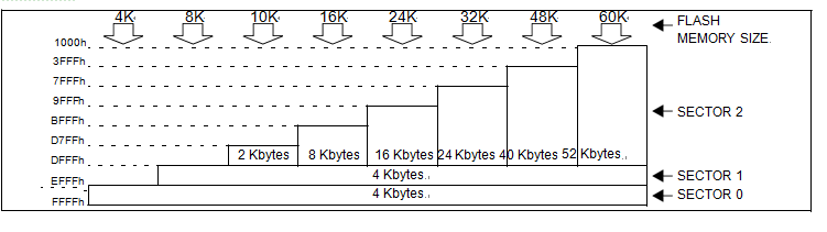
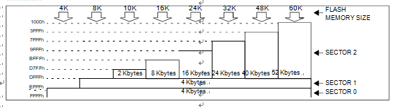
The Flash memory is organised in sectors and can be used for both code and data storage.
Depending on the overall Flash memory size in the micro-controller device, there are up to three user sectors (see below Table). Each of these sectors can be erased independently to avoid unnecessary erasing of the whole Flash memory when only a partial erasing is required after breaking st72f32ak1 mcu flash memory protection.
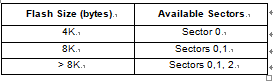
The first two sectors have a fixed size of 4 Kbytes (see below Figure). They are mapped in the upper part of the ST7 addressing space so the reset and in- terrupt vectors are located in Sector 0 (F000h- FFFFh).
3.5.1 Power supply schemes
- VDD = 2.4 to 3.6 V: external power supply for I/Os and the internal regulator. Provided externally through VDD pins.
- VDDA = from VDD to 3.6 V: external analog power supply for ADC, Reset blocks, RCs and PLL. The VDDA voltage level must be always greater or equal to the VDD voltage level and must be provided first.
Decrypt ST72F321BK MCU Flash Memory Program
Decrypt ST72F321BK MCU Flash Memory Program is a process to pull the embedded firmware from st72f321bk mcu flash memory and then copy the heximal to new microcontroller;
The ST7 dual voltage High Density Flash (HDFlash) is a non-volatile memory that can be electrically erased as a single block or by individu- al sectors and programmed on a Byte-by-Byte ba- sis using an external VPP supply.
The HDFlash devices can be programmed and erased off-board (plugged in a programming tool) or on-board using ICP (In-Circuit Programming) or IAP (In-Application Programming) which can be applied for breaking mcu st72f321j9 flash memory.
The array matrix organisation allows each sector to be erased and reprogrammed without affecting other sectors.
- Three Flash programming modes:
- Insertion in a programming tool. In this mode, all sectors including option bytes can be pro- grammed or erased.
- ICP (In-Circuit Programming). In this mode, all sectors including option bytes can be pro- grammed or erased without removing the de- vice from the application board.
- IAP (In-Application Programming) In this mode, all sectors except Sector 0, can be pro- grammed or erased without removing the de- vice from the application board and while the application is running.
- ICT (In-Circuit Testing) for downloading and executing user application test patterns in RAM when attacking st72f321ar mcu protected flash memory
- Read-out protection
- Register Access Security System (RASS) to prevent accidental programming or erasing