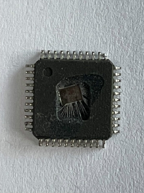
 Break ST72F321J9 Microcontroller Flash/ROM Memory
Break ST72F321J9 Microcontroller Flash/ROM Memory and extract embedded data from secured flash controlled by microprocessor ST72F321J9, and then crack secured mcu st72f321j9 security fuse bit;
PIN DESCRIPTION (Cont’d)
For external pin connection guidelines, refer to See “ELECTRICAL CHARACTERISTICS” on page 113.
Legend / Abbreviations for Table 1:
Type: I = input, O = output, S = supply
Input level: A = Dedicated analog input In/Output level: C = CMOS 0.3VDD/0.7VDD
CT= CMOS 0.3VDD/0.7VDD with input trigger Output level:
HS = 20mA high sink (on N-buffer only)
Port and control configuration:
- Input:
- float = floating, wpu = weak pull-up, int = interrupt 1), ana = analog ports
- Output: OD = open drain 2), PP = push-pull
Refer to “I/O PORTS” on page 42 for more details on the software configuration of the I/O ports.
The RESET configuration of each pin is shown in bold. This configuration is valid as long as the device is in reset state.
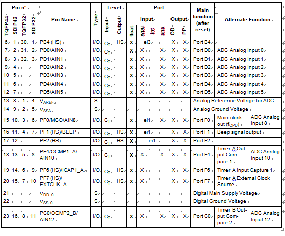
- In the interrupt input column, “eiX” defines the associated external interrupt vector. If the weak pull-up column (wpu) is merged with the interrupt column (int) when breaking st72f32ak1 microcontroller flash memory, then the I/O configuration is pull-up interrupt input, else the configuration is floating interrupt input.
- In the open drain output column, “T” defines a true open drain I/O (P-Buffer and protection diode to VDD are not implemented). See See “I/O PORTS” on page 42. and Section 12.8 I/O PORT PIN CHARACTER- ISTICS for more details.
- OSC1 and OSC2 pins connect a crystal/ceramic resonator, or an external source to the on-chip oscil- lator; see Section 1 INTRODUCTION and Section 12.5 CLOCK AND TIMING CHARACTERISTICS for more details.
- On the chip, each I/O port has 8 pads. Pads that are not bonded to external pins are in input pull-up configuration after reset and restore st72f32ak2 mcu encrypted flash heximal. The configuration of these pads must be kept at reset state to avoid added current consumption.