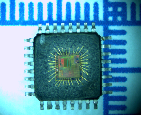
 ST Microcomputer ST72F340K2 Flash Program Memory Unlocking
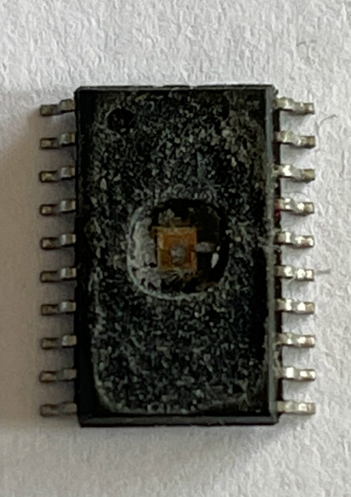
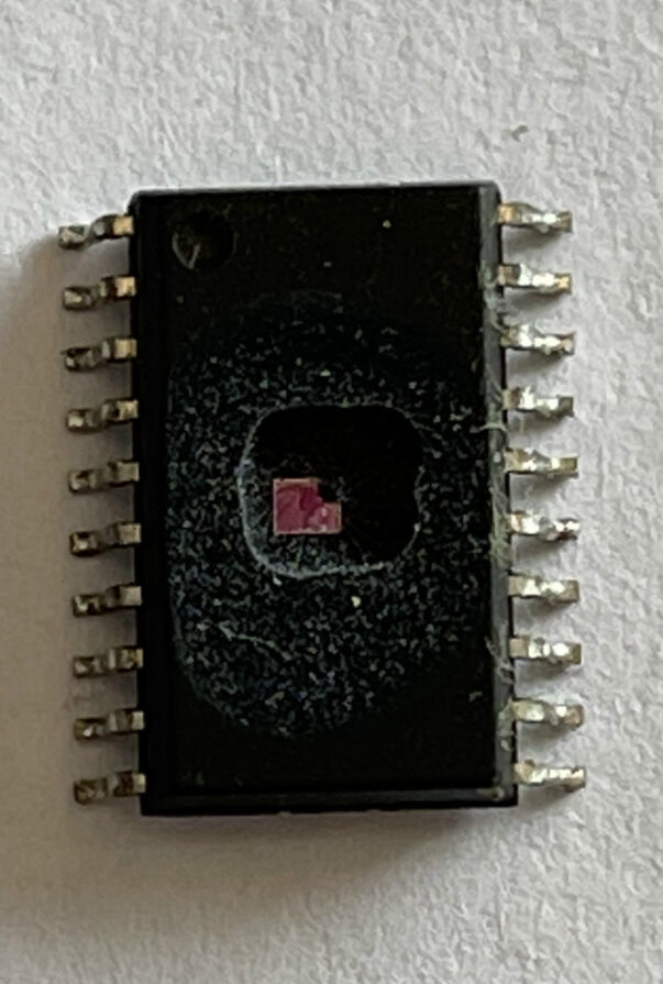
ST Microcomputer ST72F340K2 Flash Program Memory Unlocking needs to disable the fuse bit of tamper resistance system and readout embedded firmware from Microcontroller, pull extracted heximal to new st72f340k2 microprocessor flash memory;
To perform ICP the microcontroller must be switched to ICC (In-Circuit Communication) mode by an external controller or programming tool.
Depending on the ICP code downloaded in RAM, Flash memory programming can be fully customized (number of bytes to program, program locations, or selection serial communication interface for downloading) when copy embedded binary firmware to new microcontroller st72f325s6.
When using an STMicroelectronics or third-party programming tool that supports ICP and the specific microcontroller device, the user needs only to implement the ICP hardware interface on the application board (see below Figure). For more details on the pin locations, refer to the device pinout description.
This mode uses a BootLoader program previously stored in Sector 0 by the user (in ICP mode or by plugging the device in a programming tool). This mode is fully controlled by user software in the process of cloning st72f325k4 secured microcontroller flash memory content. This allows it to be adapted to the user application, (us- er-defined strategy for entering programming mode, choice of communications protocol used to fetch the data to be stored, etc.).
NXP Locked Microcontroller SPC5604PGF1VLQ6 Flash Data Duplication
NXP Locked Microcontroller SPC5604PGF1VLQ6 Flash Data Duplication needs to crack spc5604pgf1vl mcu protective system and extract embedded flash binary from microcomputer’s memory:
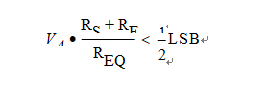
In fact a current sink contributor is represented by the charge sharing effects with the sampling capacitance: being CS and Cp2 substantially two switched capacitances, with a frequency equal to the conversion rate of the ADC, it can be seen as a resistive path to ground when recover spc5603bk microcomputer flash file.
For instance, assuming a conversion rate of 1 MHz, with CS+Cp2 equal to 3 pF, a resistance of 330 kW is obtained (REQ = 1 / (fc × (CS+Cp2)), where fc represents the conversion rate at the considered channel). To minimize the error induced by the voltage partitioning between this resistance (sampled voltage on CS+Cp2) and the sum of RS + RF, the external circuit must be designed to respect the below Equation:
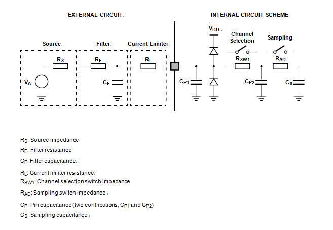
A second aspect involving the capacitance network shall be considered. Assuming the three capacitances CF, CP1 and CP2 are initially charged at the source voltage VA (refer to the equivalent circuit in Figure 13): A charge sharing phenomenon is installed when the sampling phase is started (A/D switch close).
NXP Microcontroller SPC5604BK0CLQ6 Flash Memory Content Replicating
NXP Microcontroller SPC5604BK0CLQ6 Flash Memory Content Replicating needs to unlock microprocessor spc5604bk0cl security fuse bit and then copy embedded data from MCU flash memory;
In the following analysis, the input circuit corresponding to the precise channels is considered.
To preserve the accuracy of the A/D converter, it is necessary that analog input pins have low AC impedance. Placing a capacitor with good high frequency characteristics at the input pin of the device can be effective: the capacitor should be as large as possible, ideally infinite especially in the process of copy spc5602pef01m secured mcu flash binary code.
This capacitor contributes to attenuating the noise present on the input pin; furthermore, it sources charge during the sampling phase, when the analog signal source is a high-impedance source.
A real filter can typically be obtained by using a series resistance with a capacitor on the input pin (simple RC filter). The RC filtering may be limited according to the value of source impedance of the transducer or circuit supplying the analog signal to be measured only after the spc5602 microcomputer encrypted flash memory data being cloning.
The filter at the input pins must be designed taking into account the dynamic characteristics of the input signal (bandwidth) and the equivalent input impedance of the ADC itself.

Freescale SPC5603CK0CLL6 Microcontroller Flash Content Restoration
Freescale SPC5603CK0CLL6 Microcontroller Flash Content Restoration is a process starting from decapsulate silicon package of microcontroller to remove the first layer of protection, and use MCU cracking technique to disable the protection over the microprocessor spc5603ck0 flash memory, and extract embedded binary file from microcomputer flash memory;
- eMIOS: instance: 0 ON (16 channels on PA[0]–PA[11] and PC[12]–PC[15]) with PWM 20 kHz, instance: 1 clock gated. DSPI: instance: 0 (clocked but no communication). RTC/API ON.PIT ON. STM ON. ADC ON but no conversion except 2 analog watchdogs.
- Only for the “P” classification: No clock, FIRC (16 MHz) off, SIRC (128 kHz) on, PLL off, HPVreg off, ULPVreg/LPVreg on. All possible peripherals off and clock gated. Flash in power down mode can be used to recover microcomputer spc5603bk flash binary file.
- 3 When going from RUN to STOP mode and the core consumption is > 6 mA, it is normal operation for the main regulator module to be kept on by the on-chip current monitoring circuit. This is most likely to occur with junction temperatures exceeding 125 °C and under these circumstances when readout spc5601df1 microcontroller on chip flash memory content, it is possible for the current to initially exceed the maximum STOP specification by up to 2 mA. After entering stop, the application junction temperature will reduce to the ambient level and the main regulator will be automatically switched off when the load current is below 6 mA.
- Only for the “P” classification: ULPVreg on, HP/LPVreg off, 16 KB SRAM on, device configured for minimum consumption, all possible modules switched off.
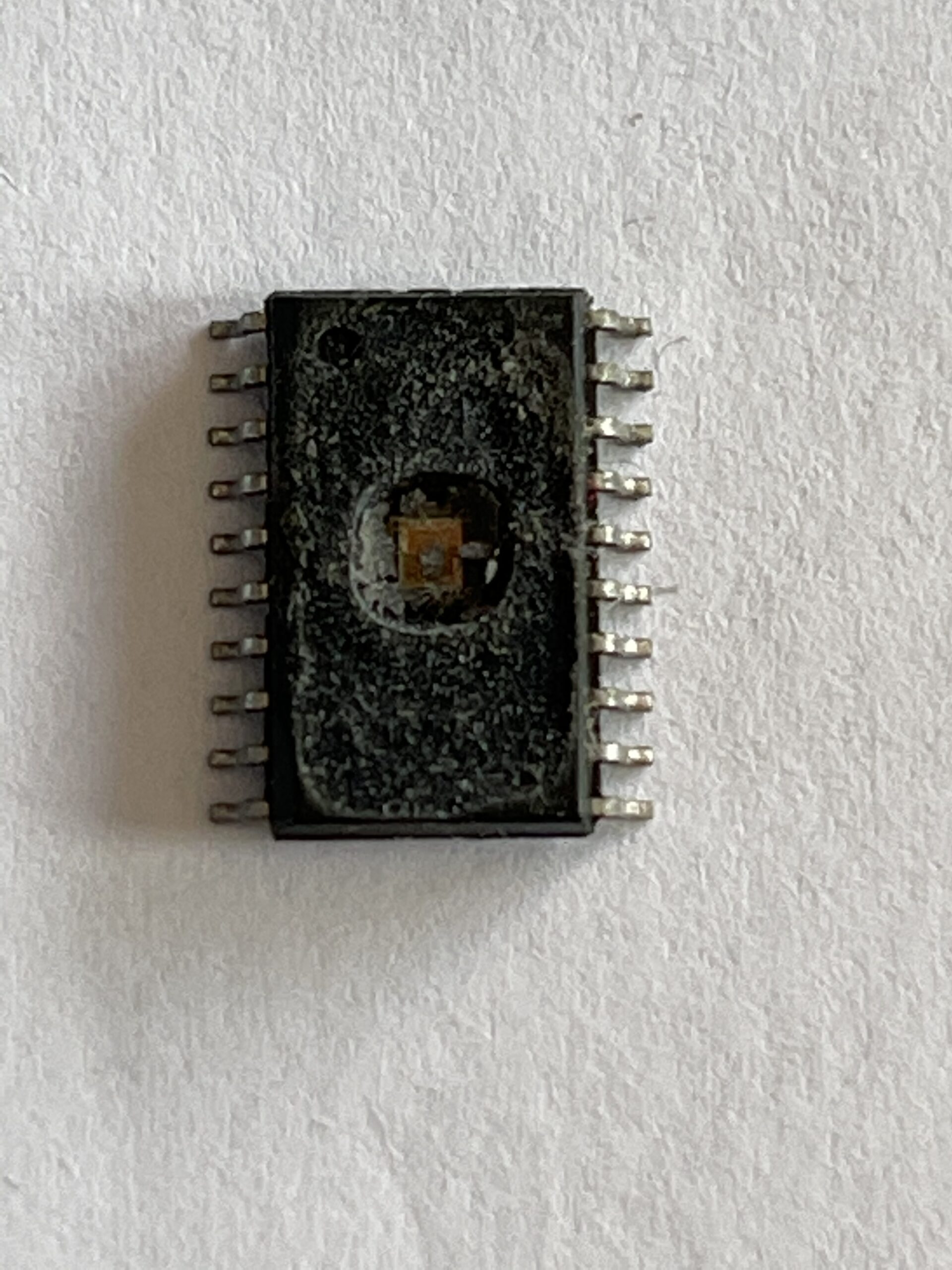
Recover NXP SPC5603BK0CLQ4R Microcomputer Flash File
Recover NXP SPC5603BK0CLQ4R Microcomputer Flash File needs to crack mcu spc5603bk0cl protective system and copy the binary file to new microcontroller spc5603bk samples;
- VDD = 3.3 V ± 10% / 5.0 V ± 10%, TA = -40 to 125 °C, unless otherwise specified
- Running consumption does not include I/Os toggling which is highly dependent on the application. The given value is thought to be a worst case value with all peripherals running, and code fetched from code flash while modify
operation ongoing on data flash. Notice that this value can be significantly reduced by application: switch off not used peripherals (default), reduce peripheral frequency through internal prescaler, fetch from RAM most used functions, use low power mode when copy nxp secured mcu spc5602pef flash binary file.
- Higher current may be sinked by device during power-up and standby exit. Please refer to in-rush average current on Table 23.
- RUN current measured with typical application with accesses on both flash memory and SRAM.
- Only for the “P” classification: Code fetched from SRAM: serial IPs CAN and LIN in loop-back mode, DSPI as Master, PLL as system clock (3 × Multiplier) peripherals on (eMIOS/CTU/ADC) and running at maximum frequency, periodic SW/WDG timer reset enabled.
Data flash power down. Code flash in low power. SIRC (128 kHz) and FIRC (16 MHz) on. 10 MHz XTAL clock. FlexCAN: 0 ON (clocked but no reception or transmission). LINFlex: instances: 0, 1, 2 ON (clocked but no reception or transmission), instance: 3 clocks gated in the process of cloning spc5602df1v encrypted mcu flash code.
Freescale Encrypted MCU SPC5602DF1VLH4R Flash Data Cloning
Freescale Encrypted MCU SPC5602DF1VLH4R Flash Data Cloning means the embedded firmware from original Microcontroller spc5602df1 will be unlocked and extract the binary file directly from opened microprocessor;
The device provides four main I/O pad types depending on the associated alternate functions:
Slow pads—These pads are the most common pads, providing a good compromise between transition time and low electromagnetic emission.
Medium pads—These pads provide transition fast enough for the serial communication channels with controlled current to reduce electromagnetic emission when copying spc5602pef0m1 secured mcu flash binary.
Input only pads—These pads are associated to ADC channels (ADC_P[X]) providing low input leakage.
Medium pads can use slow configuration to reduce electromagnetic emission except for PC[1], that is medium only, at the cost of reducing AC performance in order to reading out spc5601df1m1 microcontroller flash content.
TABLE : I/O input DC electrical characteristics
| Symbol | C | Parameter | Conditions1 | Value | Unit | ||||
| Min | Typ | Max | |||||||
| VIH | SR | P | Input high level CMOS (Schmitt Trigger) | — | 0.65VDD | — | VDD+0.4 | V | |
| VIL | SR | P | Input low level CMOS (Schmitt Trigger) | — | -0.4 | — | 0.35VDD | V | |
| VHYS | CC | C | Input hysteresis CMOS (Schmitt Trigger) | — | 0.1VDD | — | — | V | |
| ILKG | CC | D | Digital input leakage | No injection on adjacent pin | TA = -40 °C | — | 2 | 200 | nA |
| D | TA = 25 °C | — | 2 | 200 | |||||
| D | TA = 85 °C | — | 5 | 300 | |||||
| D | TA = 105 °C | — | 12 | 500 | |||||
| P | TA = 125 °C | — | 70 | 1000 | |||||
| WFI2 | SR | P | Digital input filtered pulse | — | — | — | 40 | ns | |
| (2) WNFI | SR | P | Digital input not filtered pulse | — | 1000 | — | — | ns |
VDD = 3.3 V ± 10% / 5.0 V ± 10%, TA = -40 to 125 °C, unless otherwise specified
2 In the range from 40 to 1000 ns, pulses can be filtered or not filtered, according to operating temperature and voltage.
| Symbol | C | Parameter | Conditions1 | Value | Unit | ||||
| Min | Typ | Max | |||||||
| |IWPU| | CC | P | Weak pull-up current absolute value | VIN = VIL, VDD = 5.0 V ± 10% | PAD3V5V = 0 | 10 | — | 150 | µA |
| C | PAD3V5V = 12 | 10 | — | 250 | |||||
| P | VIN = VIL, VDD = 3.3 V ± 10% | PAD3V5V = 1 | 10 | — | 150 | ||||
| |IWPD| | CC | P | Weak pull-down current absolute value | VIN = VIH, VDD = 5.0 V ± 10% | PAD3V5V = 0 | 10 | — | 150 | µA |
| C | PAD3V5V = 1(2) | 10 | — | 250 | |||||
| P | VIN = VIH, VDD = 3.3 V ± 10% | PAD3V5V = 1 | 10 | — | 150 |
- VDD = 3.3 V ± 10% / 5.0 V ± 10%, TA = -40 to 125 °C, unless otherwise specified.
- 2 The configuration PAD3V5 = 1 when VDD = 5 V is only a transient configuration during power-up. All pads but RESET are configured in input or in high impedance state.
NXP Secured MCU SPC5602PEF0MLH6 Flash Binary Copying
NXP Secured MCU SPC5602PEF0MLH6 Flash Binary Copying needs to crack nxp locked microprocessor security fuse bit by focus ion beam and then extract embedded firmware from micro-controller’s flash memory;
The electrical parameters shown in this supplement are guaranteed by various methods. To give the customer a better understanding, the classifications listed in below Table are used and the parameters are tagged accordingly in the tables where appropriate.
| Classification tag | Tag description |
| P | Those parameters are guaranteed during production testing on each individual device. |
| C | Those parameters are achieved by the design characterization by measuring a statistically relevant sample size across process variations. |
| T | Those parameters are achieved by design characterization on a small sample size from typical devices under typical conditions unless otherwise noted. All values shown in the typical column are within this category. |
| D | Those parameters are derived mainly from simulations. |
Bit values in the Non-Volatile User Options (NVUSRO) Register control portions of the device configuration, namely electrical parameters such as high voltage supply and oscillator margin to readout the embedded flash content from microprocessor spc5601df1, as well as digital functionality (watchdog enable/disable after reset). For a detailed description of the NVUSRO register, please refer to the device reference manual.
The DC electrical characteristics are dependent on the PAD3V5V bit value. Table 7 shows how NVUSRO[PAD3V5V] controls the device configuration.
Table 7. PAD3V5V field description
| Value1 | Description |
| 0 | High voltage supply is 5.0 V |
| 1 | High voltage supply is 3.3 V |
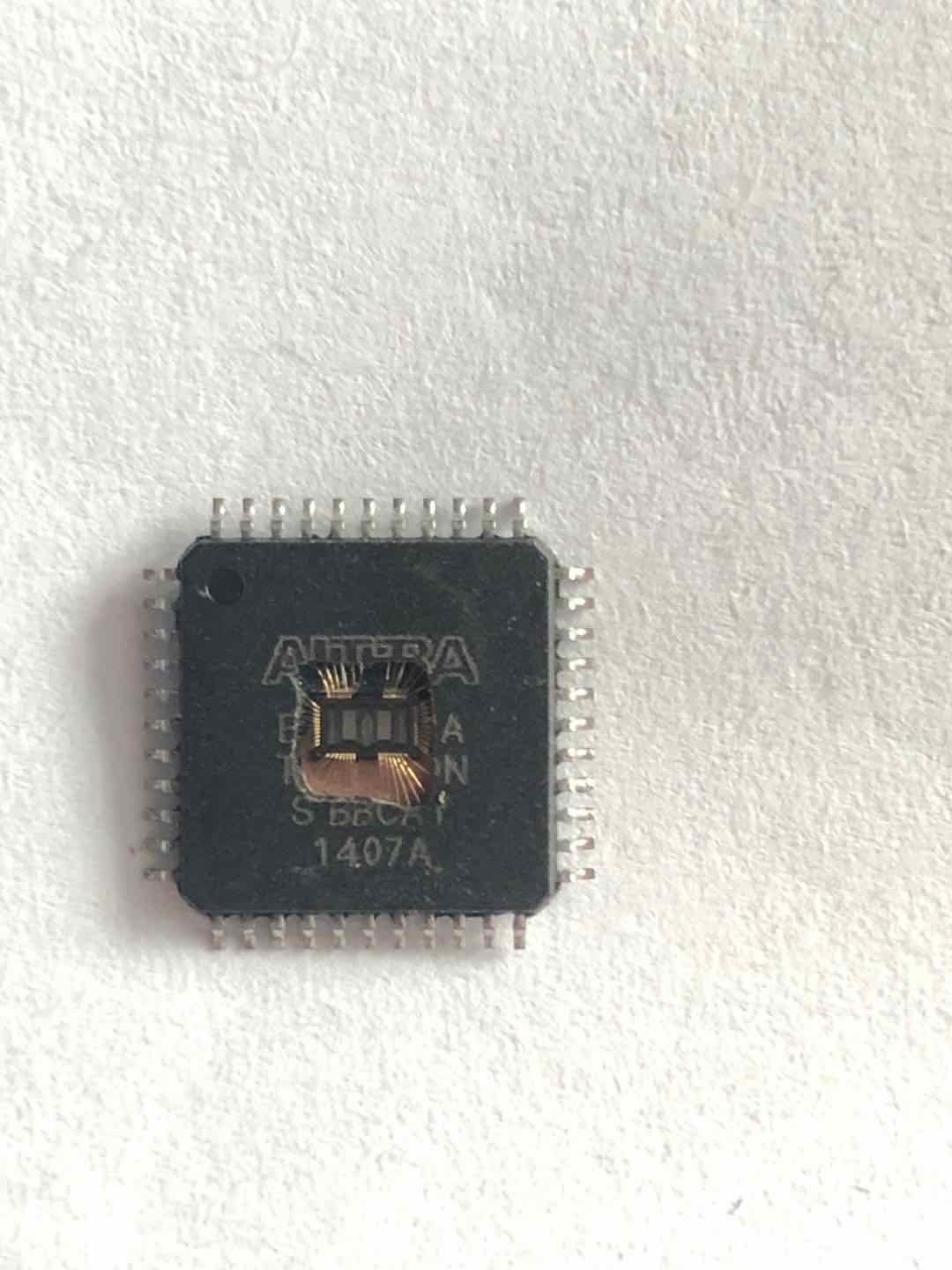
NXP Automobile 32 Bit Microprocessor SPC5601PEF Flash Data Extraction
NXP Automobile 32 Bit Microprocessor SPC5601PEF Flash Data Extraction is a process to unlock system on chip secured microcontroller locking bits, and copy extracted firmware from both code flash and data flash to new NXP MCU;
Up to 79 configurable general purpose pins supporting input and output operations (package dependent)
Real Time Counter (RTC) with clock source from 128 kHz or 16 MHz internal RC oscillator supporting autonomous wakeup with 1 ms resolution with max timeout of 2 seconds
Up to 4 periodic interrupt timers (PIT) with 32-bit counter resolution
1 System Timer Module (STM)
Nexus development interface (NDI) per IEEE-ISTO 5001-2003 Class 1 standard
Device/board boundary Scan testing supported with per Joint Test Action Group (JTAG) of IEEE (IEEE 1149.1)
On-chip voltage regulator (VREG) for regulation of input supply for all internal levels.
These 32-bit automotive microcontrollers are a family of system-on-chip (SoC) devices designed to be central to the development of the next wave of central vehicle body controller, smart junction box, front module, peripheral body, door control and seat control applications.
This family is one of a series of next-generation integrated automotive microcontrollers based on the Power Architecture technology and designed specifically for embedded applications especially for cracking microcontroller locked bit by focus ion beam.
The advanced and cost-efficient e200z0h host processor core of this automotive controller family complies with the Power Architecture technology and only implements the VLE (variable-length encoding) APU (auxiliary processing unit), providing improved code density.
It operates at speeds of up to 48 MHz and offers high performance processing optimized for low power consumption. It capitalizes on the available development infrastructure of current Power Architecture devices and is supported with software drivers, operating systems and configuration code to assist with the user’s implementations after reverse engineering mcu embedded heximal from flash memory.
The device platform has a single level of memory hierarchy and can support a wide range of on-chip static random access memory (SRAM) and internal flash memory.
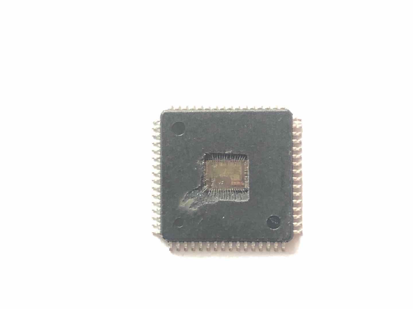
Readout Freescale SPC5601DF1MLL4 Microcontroller on chip Flash Content
Readout Freescale SPC5601DF1MLL4 Microcontroller on chip Flash Content needs to disable the tamper resistance of 32-BIT MCU SPC5601DF1M through breaking microcontroller, and then dump the embedded firmware from CPU flash memory.
Single issue, 32-bit CPU core complex (e200z0h)
Compliant with the Power Architecture® embedded category
Includes an instruction set enhancement allowing variable length encoding (VLE) for code size footprint reduction. With the optional encoding of mixed 16-bit and 32-bit instructions, it is possible to achieve significant code size footprint reduction.
Up to 256 KB on-chip Code Flash supported with Flash controller and ECC
64 KB on-chip Data Flash with ECC
Up to 16 KB on-chip SRAM with ECC
Interrupt controller (INTC) with multiple interrupt vectors, including 20 external interrupt sources and 18 external interrupt/wakeup sources
Frequency modulated phase-locked loop (FMPLL)
Crossbar switch architecture for concurrent access to peripherals, Flash, or SRAM from multiple bus masters by recover freescale mcu flash memory program;
Boot assist module (BAM) supports internal Flash programming via a serial link (CAN or SCI)
Timer supports input/output channels providing a range of 16-bit input capture, output compare, and pulse width modulation functions (eMIOS-lite)
Up to 33 channel 12-bit analog-to-digital converter (ADC)
2 serial peripheral interface (DSPI) modules
3 serial communication interface (LINFlex) modules
LINFlex 1 and 2: Master capable
LINFlex 0: Master capable and slave capable; connected to eDMA
1 enhanced full CAN (FlexCAN) module with configurable buffers
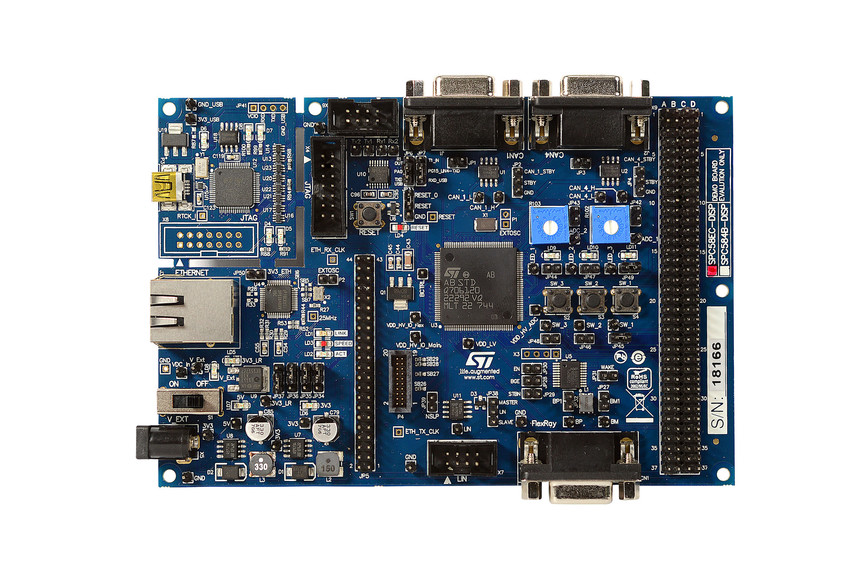
The STM32F030x4/x6/x8/xC microcontrollers include devices in four different packages ranging from 20 pins to 64 pins. Depending on the device chosen, different sets of peripherals are included. The description below provides an overview of the complete range of STM32F030x4/x6/x8/xC peripherals proposed. These features make the STM32F030x4/x6/x8/xC microcontrollers suitable for a wide range of applications such as application control and user interfaces, handheld equipment, A/V receivers and digital TV, PC peripherals, gaming and GPS platforms, industrial applications, PLCs, inverters, printers, scanners, alarm systems, video intercoms, and HVACs.
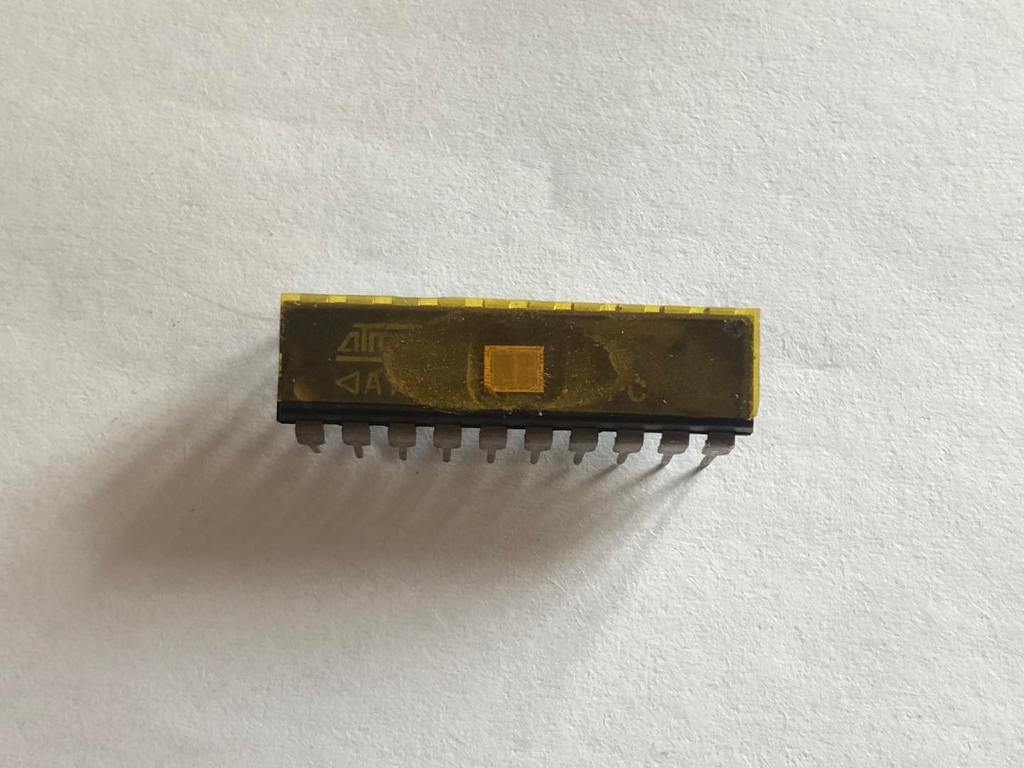
Readout STM ST72F325R9 Microcomputer Flash Memory Software
Readout STM ST72F325R9 Microcomputer Flash Memory Software needs to unlock st72f325r9 secured microprocessor tamper resistance system and copy extracted firmware to new MCU which can provide the exact functions as original Microcontroller;
- If the ICCCLK or ICCDATA pins are only used as outputs in the application, no signal isolation is necessary. As soon as the Programming Tool is plugged to the board, even if an ICC session is not in progress, the ICCCLK and ICCDATA pins are not available for the application.
- If they are used as inputs by the application, isolation such as a serial resistor has to implemented in case another de- vice forces the signal. Refer to the Programming Tool documentation for recommended resistor values when break st32f321k9 mcu flash and ROM memory protection.
- During the ICC session, the programming tool must control the RESET pin. This can lead to conflicts between the programming tool and the application reset circuit if it drives more than 5mA at high level (push pull output or pull-up resistor<1K).
- A schottky diode can be used to isolate the appli- cation RESET circuit in this case. When using a classical RC network with R>1K or a reset management IC with open drain output and pull-up resistor>1K, no additional components are needed. In all cases the user must ensure that no external reset is generated by the application during the ICC session.
- The use of Pin 7 of the ICC connector depends on the Programming Tool architecture. This pin must be connected when using most ST Program- ming Tools (it is used to monitor the application power supply). Please refer to the Programming Tool manual after unlocking st32f324bj microprocessor program flash memory.
Pin 9 has to be connected to the OSC1 or OS-CIN pin of the ST7 when the clock is not available in the application or if the selected clock option is not programmed in the option byte. ST7 devices with multi-oscillator capability need to have OSC2 grounded in this case.