 Recover MCU ATmega644PA Flash
 December 11th, 2010 |
  Author:
 Recover MCU ATmega644PA Flash memory content after crack microcontroller ATmega644PA protection and extract code from microprocessor ATmega644PA memory.
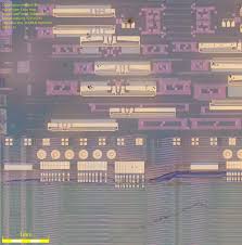
When the BOD is enabled, and VCC decreases to a value below the trigger level (VBOT- in Figure 29), the Brown-out Reset is immediately activated. When VCC increases above the trigger level (VBOT+ in Figure 29), the delay counter starts the MCU after the Time- out period tTOUT has expired if recover mcu pic18f452 program.
The BOD circuit will only detect a drop in VCC if the voltage stays below the trigger level for longer than tBOD given in Table 23. When the Watchdog times out, it will generate a short reset pulse of one CK cycle duration.
On the falling edge of this pulse, the delay timer starts counting the Time-out period tTOUT. See “Watchdog Timer” on page 56. for details on operation of the Watchdog Timer after break chip pic12cr509a flash.
ATmega644PA features an internal bandgap reference. This reference is used for Brown-out Detection, and it can be used as an input to the Analog Comparator or the ADC.
The voltage reference has a start-up time that may influence the way it should be used. The start-up time is given in Table 26. To save power, the reference is not always turned The reference is on during the following situations if attack dsp mcu tms320f241pg heximal:
When the BOD is enabled (by programming the BODLEVEL [2..0] Fuse).
When the bandgap reference is connected to the Analog Comparator (by setting the ACBG bit in ACSR) before recover mcu flash. When the ADC is enabled.
Thus, when the BOD is not enabled, after setting the ACBG bit or enabling the ADC, the user must always allow the reference to start up before the output from the Analog Comparator or ADC is used.
To reduce power consumption in Power-down mode, the user can avoid the three conditions above to ensure that the reference is turned off before entering Power-down mode when recover mcu flash. ATmega644PA has an Enhanced Watchdog Timer (WDT). The main features are:
Clocked from separate On-chip Oscillator
3 Operating modes
– Interrupt
– System Reset
– Interrupt and System Reset
 Posted in Recover Chip |
  Tags: recover mcu protected archive, recover mcu protected code, recover mcu protected content, recover mcu protected data, recover mcu protected eeprom, recover mcu protected file, recover mcu protected firmware, recover mcu protected information, recover mcu protected memory, recover mcu protected program |
  Comments Closed
Reverse Engineering IC ATmega644A Firmware
Reverse Engineering IC ATmega644A and clone ATmega644A microcontroller firmware from embedded flash and eeprom memory;
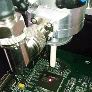
If the On-chip debug system is enabled by the OCDEN Fuse and the chip enters sleep mode, the main clock source is enabled, and hence, always consumes power. In the deeper sleep modes, this will contribute significantly to the total current consumption.
There are three alternative ways to disable the OCD system: Disable the OCDEN Fuse. Disable the JTAGEN Fuse. Write one to the JTD bit in MCUCR.
During reset, all I/O Registers are set to their initial values, and the program starts execution from the Reset Vector. The instruction placed at the Reset Vector must be a JMP – Absolute Jump – instruction to the reset handling routine.
If the program never enables an interrupt source, the Interrupt Vectors are not used, and regular program firmware can be placed at these locations. This is also the case if the Reset Vector is in the Application section while the Interrupt Vectors are in the Boot section or vice versa before attack microcontroller mc68hc705p6 bin.
The circuit diagram in Figure 25 shows the reset logic. Table 23 defines the electrical parameters of the reset circuitry. The I/O ports of the AVR are immediately reset to their initial state when a reset source goes active. This does not require any clock source to be running if attack chip st62t00cb6 firmware.
After all reset sources have gone inactive, a delay counter is invoked, stretching the internal reset. This allows the power to reach a stable level before normal operation starts. The time-out period of the delay counter is defined by the user through the SUT and CKSEL Fuses. The different selections for the delay period are presented in “Clock Sources”.
The ATmega644 has five sources of reset: Power-on Reset. The MCU is reset when the supply voltage is below the Power-on Reset threshold (VPOT). External Reset. The MCU is reset when a low level is present on the RESET pin for longer than the minimum pulse length before copy mcu pic18f2480 program.
Watchdog Reset. The MCU is reset when the Watchdog Timer period expires and the Watchdog is enabled. Brown-out Reset. The MCU is reset when the supply voltage VCC is below the Brown-out Reset threshold (VBOT) and the Brown-out Detector is enabled.
JTAG AVR Reset. The MCU is reset as long as there is a logic one in the Reset Register, one of the scan chains of the JTAG system. Refer to the section “IEEE 1149.1 (JTAG) Boundary-scan” on page 301 for details.
A Power-on Reset (POR) pulse is generated by an On-chip detection circuit. The detection level is defined in Table 23. The POR is activated whenever VCC is below the detection level. The POR circuit can be used to trigger the start-up Reset, as well as to detect a failure in supply voltage.
A Power-on Reset (POR) circuit ensures that the device is reset from Power-on. Reaching the Power-on Reset threshold voltage invokes the delay counter, which determines how long the device is kept in RESET after VCC rise. The RESET signal is activated again, without any delay, when VCC decreases below the detection level.
An External Reset is generated by a low level on the RESET pin. Reset pulses longer than the minimum pulse width (see Table 23) will generate a reset, even if the clock is not running. Shorter pulses are not guaranteed to generate a reset. When the applied signal reaches the Reset Threshold Voltage – VRST – on its positive edge, the delay counter starts the MCU after the Time-out period – tTOUT – has expired.
ATmega644 has an On-chip Brown-out Detection (BOD) circuit for monitoring the VCC level during operation by comparing it to a fixed trigger level. The trigger level for the BOD can be selected by the BODLEVEL Fuses. The trigger level has a hysteresis to ensure spike free Brown-out Detection. The hysteresis on the detection level should be interpreted as VBOT+ = VBOT + VHYST/2 and VBOT- = VBOT – VHYST/2.
Posted in Reverse Engineer Microcontroller |
Tags: reverse engineering ic protected archive, reverse engineering IC protected binary, reverse engineering ic protected code, reverse engineering IC protected content, reverse engineering IC protected data, reverse engineering ic protected eeprom, reverse engineering IC protected file, reverse engineering ic protected firmware, reverse engineering IC protected heximal, reverse engineering ic protected information, reverse engineering ic protected memory, reverse engineering ic protected program |
Comments Closed
Recover MCU ATmega644 Code
Recover MCU ATmega644 Code from secured program memory, the code of ATmega644 will be extracted by cracking ATmega644 security fuse bit;
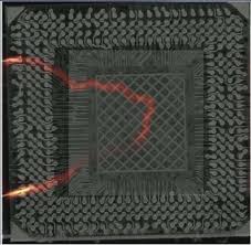
There are several issues to consider when trying to minimize the power consumption in an AVR controlled system. In general, sleep modes should be used as much as possible, and the sleep mode should be selected so that as few as possible of the device’s functions are operating when Recover Mcu.
All functions not needed should be disabled. In particular, the following modules may need special consideration when trying to achieve the lowest possible power consumption.
If enabled, the ADC will be enabled in all sleep modes. To save power, the ADC should be disabled before entering any sleep mode. When the ADC is turned off and on again, the next conversion will be an extended conversion. Refer to “Analog to Digital Converter” on page 274 for details on ADC operation before break IC SST89E58RD2 software.
When entering Idle mode, the Analog Comparator should be disabled if not used. When entering ADC Noise Reduction mode, the Analog Comparator should be disabled. In other sleep modes, the Analog Comparator is automatically disabled after Recover MCU dspic30f6013a firmware.
However, if the Analog Comparator is set up to use the Internal Voltage Reference as input, the Analog Comparator should be disabled in all sleep modes. Otherwise, the Internal Voltage Reference will be enabled, independent of sleep mode. Refer to “Analog Comparator” on page 271 for details on how to configure the Analog Comparator.
If the Brown-out Detector is not needed by the application, this module should be turned off. If the Brown-out Detector is enabled by the BODLEVEL Fuses, it will be enabled in all sleep modes, and hence, always consume power. In the deeper sleep modes, this will contribute significantly to the total current consumption when break Mcu at89c5131a bin.
Refer to “Brown-out Detection” on page 59 for details on how to configure the Brown-out Detector.
The Internal Voltage Reference will be enabled when needed by the Brown-out Detection, the Analog Comparator or the ADC. If these modules are disabled as described in the sections above, the internal voltage reference will be disabled and it will not be consuming power.
When turned on again, the user must allow the reference to start up before the output is used. If the reference is kept on in sleep mode, the output can be used immediately. Refer to “Internal Voltage Reference” on page 62 for details on the start-up time.
If the Watchdog Timer is not needed in the application, the module should be turned off. If the Watchdog Timer is enabled, it will be enabled in all sleep modes, and hence, always consume power. In the deeper sleep modes, this will contribute significantly to the total current consumption. Refer to “Interrupts” on page 69 for details on how to configure the Watchdog Timer.
When entering a sleep mode, all port pins should be configured to use minimum power. The most important is then to ensure that no pins drive resistive loads. In sleep modes where both the I/O clock (clkI/O) and the ADC clock (clkADC) are stopped, the input buffers of the device will be disabled.
This ensures that no power is consumed by the input logic when not needed. In some cases, the input logic is needed for detecting wake-up conditions, and it will then be enabled. Refer to the section “Digital Input Enable and Sleep Modes” on page 85 for details on which pins are enabled.
If the input buffer is enabled and the input signal is left floating or have an analog signal level close to VCC/2, the input buffer will use excessive power. For analog input pins, the digital input buffer should be disabled at all times. An analog signal level close to VCC/2 on an input pin can cause significant current even in active mode.
Digital input buffers can be disabled by writing to the Digital Input Disable Registers (DIDR2, DIDR1 and DIDR0). Refer to “Digital Input Disable Register 2 – DIDR2” on page 293, “Digital Input Disable Register 1 – DIDR1” on page 273 and “Digital Input Disable Register 0 – DIDR0” on page 293 for details.
Posted in Reverse Engineer Microcontroller |
Tags: recover mcu protected archive, recover mcu protected bin, recover mcu protected code, recover mcu protected content, recover mcu protected data, recover mcu protected eeprom, recover mcu protected file, recover mcu protected firmware, recover mcu protected hex, recover mcu protected information, recover mcu protected memory, recover mcu protected program |
Comments Closed
Extract Chip ATmega324PA Code
Extract Chip ATmega324PA Code from embedded program memory after unlock chip atmega324pa.
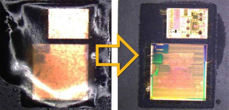
Bit 7 – PRTWI: Power Reduction TWI
Writing a logic one to this bit shuts down the TWI by stopping the clock to the module. When waking up the TWI again, the TWI should be re initialized to ensure proper operation.
Bit 6 – PRTIM2: Power Reduction Timer/Counter2
Writing a logic one to this bit shuts down the Timer/Counter2 module in synchronous mode (AS2 is 0). When the Timer/Counter2 is enabled, operation will continue like before the shutdown if recover mcu atmega164pa code.
Bit 5 – PRTIM0: Power Reduction Timer/Counter0
Writing a logic one to this bit shuts down the Timer/Counter0 module. When the Timer/Counter0 is enabled, operation will continue like before the shutdown.
Bit 4 – Res: Reserved bit
This bit is reserved bit and will always read as zero.
Bit 3 – PRTIM1: Power Reduction Timer/Counter1
Writing a logic one to this bit shuts down the Timer/Counter1 module. When the Timer/Counter1 is enabled, operation will continue like before the shutdown after reverse engineering chip atmega324 code.
Bit 2 – PRSPI: Power Reduction Serial Peripheral Interface
Writing a logic one to this bit shuts down the Serial Peripheral Interface by stopping the clock to the module. When waking up the SPI again, the SPI should be re initialized to ensure proper operation.
Bit 1 – PRUSART0: Power Reduction USART0
Writing a logic one to this bit shuts down the USART0 by stopping the clock to the module. When waking up the USART0 again, the USART0 should be re initialized to ensure proper operation.
Bit 0 – PRADC: Power Reduction ADC
Writing a logic one to this bit shuts down the ADC. The ADC must be disabled before shut down. The analog comparator cannot use the ADC input MUX when the ADC is shut down.
Bit 7..6 – Res: Reserved bits
These bits are reserved and will always read as zero.
Bit 5 – PRTIM5: Power Reduction Timer/Counter5
Writing a logic one to this bit shuts down the Timer/Counter5 module. When the Timer/Counter5 is enabled, operation will continue like before the shutdown if break microcontroller atmega324a bin.
Bit 4 – PRTIM4: Power Reduction Timer/Counter4
Writing a logic one to this bit shuts down the Timer/Counter4 module. When the Timer/Counter4 is enabled, operation will continue like before the shutdown.
Bit 3 – PRTIM3: Power Reduction Timer/Counter3
Writing a logic one to this bit shuts down the Timer/Counter3 module. When the Timer/Counter3 is enabled, operation will continue like before the shutdown.
Bit 2 – PRUSART3: Power Reduction USART3
Writing a logic one to this bit shuts down the USART3 by stopping the clock to the module. When waking up the USART3 again, the USART3 should be re initialized to ensure proper operation.
Bit 1 – PRUSART2: Power Reduction USART2
Writing a logic one to this bit shuts down the USART2 by stopping the clock to the module. When waking up the USART2 again, the USART2 should be re initialized to ensure proper operation.
Bit 0 – PRUSART1: Power Reduction USART1
Writing a logic one to this bit shuts down the USART1 by stopping the clock to the module. When waking up the USART1 again, the USART1 should be re initialized to ensure proper operation.
Posted in Recover Chip |
Tags: extract chip protected archive, extract chip protected binary, extract chip protected code, extract chip protected content, extract chip protected data, extract chip protected eeprom, extract chip protected file, extract chip protected firmware, extract chip protected heximal, extract chip protected information, extract chip protected memory, extract chip protected program |
Comments Closed
Break Microcontroller ATmega324A Binary
Break Microcontroller ATmega324A tamper resistance system and extract embedded binary from atmega324A and decrypt ATmega324A code to c level language;
When the SM2..0 bits are written to 010, the SLEEP instruction makes the MICROCONTROLLER enter Power-down mode. In this mode, the external Oscillator is stopped, while the external interrupts, the 2-wire Serial Interface, and the Watchdog continue operating (if enabled).
Only an External Reset, a Watchdog Reset, a Brown-out Reset, 2-wire Serial Interface address match, an external level interrupt on INT7:4, an external interrupt on INT3:0, or a pin change interrupt can wake up the MICROCONTROLLER. This sleep mode basically halts all generated clocks, allowing operation of asynchronous modules only if attack microcontroller pic18f66k90 heximal.
Note that if a level triggered interrupt is used for wake-up from Power-down mode, the changed level must be held for some time to wake up the MICROCONTROLLER. Refer to “External Interrupts” on page 75 for details.
When waking up from Power-down mode, there is a delay from the wake-up condition occurs until the wake-up becomes effective. This allows the clock to restart and become stable after having been stopped. The wake-up period is defined by the same CKSEL Fuses that define the Reset Time-out period, as described in “Clock Sources” on page 40.
When the SM2..0 bits are written to 011, the SLEEP instruction makes the MICROCONTROLLER enter Power-save mode. This mode is identical to Power-down, with one exception if copy PIC18F458 MICROCONTROLLER binary:
If Timer/Counter2 is enabled, it will keep running during sleep. The device can wake up from either Timer Overflow or Output Compare event from Timer/Counter2 if the corresponding Timer/Counter2 interrupt enable bits are set in TIMSK2, and the Global Interrupt Enable bit in SREG is set.
If Timer/Counter2 is not running, Power-down mode is recommended instead of Power-save mode.
The Timer/Counter2 can be clocked both synchronously and asynchronously in Power-save mode. If the Timer/Counter2 is not using the asynchronous clock, the Timer/Counter Oscillator is stopped during sleep. If the Timer/Counter2 is not using the synchronous clock, the clock source is stopped during sleep. Note that even if the synchronous clock is running in Power-save, this clock is only available for the Timer/Counter2.
When the SM2..0 bits are 110 and an external crystal/resonator clock option is selected, the SLEEP instruction makes the MICROCONTROLLER enter Standby mode. This mode is identical to Power-down with the exception that the Oscillator is kept running. From Standby mode, the device wakes up in six clock cycles after Break MICROCONTROLLER.
When the SM2..0 bits are 111 and an external crystal/resonator clock option is selected, the SLEEP instruction makes the MICROCONTROLLER enter Extended Standby mode. This mode is identical to Power-save mode with the exception that the Oscillator is kept running.
From Extended Standby mode, the device wakes up in six clock cycles. The Power Reduction Register, PRR, provides a method to stop the clock to individual peripherals to reduce power consumption. The current state of the peripheral is frozen and the I/O registers can not be read or written.
Resources used by the peripheral when stopping the clock will remain occupied, hence the peripheral should in most cases be disabled before stopping the clock. Waking up a module, which is done by clearing the bit in PRR, puts the module in the same state as before shutdown.
Module shutdown can be used in Idle mode and Active mode to significantly reduce the overall power consumption. See “Supply Current of IO modules” on page 381 for examples. In all other sleep modes, the clock is already stopped.
Posted in Reverse Engineer Microcontroller |
Tags: break microcontroller protected archive, break microcontroller protected code, break microcontroller protected content, break microcontroller protected data, break microcontroller protected eeprom, break microcontroller protected file, break microcontroller protected firmware, break microcontroller protected information, break microcontroller protected memory, break microcontroller protected program |
Comments Closed
Reverse Engineering IC ATmega324PV Code
Reverse Engineering IC ATmega324PV to locate the fuse bit of MCU and crack ATmega324PV for embedded memory code extraction from microcontroller ATmega324PV;
These bits define the division factor between the selected clock source and the internal system clock. These bits can be written run-time to vary the clock frequency to suit the application requirements.
As the divider divides the master clock input to the MCU, the speed of all synchronous peripherals is reduced when a division factor is used. The division factors are given in Table 20.
The CKDIV8 Fuse determines the initial value of the CLKPS bits. If CKDIV8 is unprogrammed, the CLKPS bits will be reset to “0000”.
If CKDIV8 is programmed, CLKPS bits are reset to “0011”, giving a division factor of 8 at start up. This feature should be used if the selected clock source has a higher frequency than the maximum frequency of the device at the present operating conditions after Recover chip c8051f340 firmware.
Note that any value can be written to the CLKPS bits regardless of the CKDIV8 Fuse setting. The Application software must ensure that a sufficient division factor is chosen if the selected clock source has a higher frequency than the maximum frequency of the device at the present operating conditions. The device is shipped with the CKDIV8 Fuse programmed.
Sleep modes enable the application to shut down unused modules in the MCU, thereby saving power. The AVR provides various sleep modes allowing the user to tailor the power consumption to the application’s requirements after break mcu dspic30f4011 hex.
To enter any of the five sleep modes, the SE bit in SMCR must be written to logic one and a SLEEP instruction must be executed. The SM2, SM1, and SM0 bits in the SMCR Register select which sleep mode (Idle, ADC Noise Reduction, Power-down, Power- save, or Standby) will be activated by the SLEEP instruction
The MCU is then halted for four cycles in addition to the start-up time, executes the interrupt routine, and resumes execution from the instruction following SLEEP. The contents of the Register File and SRAM are unaltered when the device wakes up from sleep. If a reset occurs during sleep mode, the MCU wakes up and executes from the Reset Vector.
Posted in Reverse Engineer Microcontroller |
Tags: reverse mcu protected archive, reverse mcu protected bin, reverse mcu protected code, reverse mcu protected content, reverse mcu protected data, reverse mcu protected eeprom, reverse mcu protected file, reverse mcu protected firmware, reverse mcu protected flash, reverse mcu protected hex, reverse mcu protected information, reverse mcu protected memory, reverse mcu protected program |
Comments Closed
Recovery MCU ATmega324V Code
Recovery MCU ATmega324V Code from flash memory, the microcontroller ATmega324V code extraction will be carried out after MCU ATmega324V cracking;
The device can utilize a 32.768 kHz watch crystal as clock source by a dedicated Low Frequency Crystal Oscillator. The crystal should be connected as shown in Figure 22.
When this Oscillator is selected, start-up times are determined by the SUT Fuses and CKSEL0 as shown in Table 13 before break PIC16F716 MCU Heximal.
The calibrated internal RC Oscillator by default provides a 8.0 MHz clock. The frequency is nominal value at 3V and 25°C. The device is shipped with the CKDIV8 Fuse programmed.
See “System Clock Prescaler” on page 48 for more details. This clock may be selected as the system clock by programming the CKSEL Fuses as shown in Table when copy pic16f886 Mcu firmware
If selected, it will operate with no external components. During reset, hardware loads the calibration byte into the OSCCAL Register and thereby automatically calibrates the RC Oscillator. At 3V and 25°C, this calibration gives a frequency of 8 MHz ± 1%.
The oscillator can be calibrated to any frequency in the range 7.3 – 8.1 MHz within ±1% accuracy, by changing the OSCCAL register.
When this Oscillator is used as the mcu clock, the Watchdog Oscillator will still be used for the Watchdog Timer and for the Reset Time-out. For more information on the pre-programmed calibration value, see the section “Calibration Byte” on page 338 before attack atmega162 Mcu flash.
The device is shipped with this option selected.
The frequency ranges are preliminary values. Actual values are TBD.
If 8 MHz frequency exceeds the specification of the device (depends on VCC); The CKDIV8 Fuse can be programmed in order to divide the internal frequency by 8. When this Oscillator is selected, start-up times are determined by the SUT Fuses.
The Oscillator Calibration Register is used to trim the Calibrated Internal RC Oscillator to remove process variations from the oscillator frequency. The factory-calibrated value is automatically written to this register during mcu reset, giving an oscillator frequency of 8.0 MHz at 25°C. The application software can write this register to change the oscillator frequency.
The oscillator can be calibrated to any frequency in the range 7.3 – 8.1 MHz within ±1% accuracy. Calibration outside that range is not guaranteed.
Note that this oscillator is used to time EEPROM and Flash write accesses, and these write times will be affected accordingly. If the EEPROM or Flash are written, do not calibrate to more than 8.8 MHz. Otherwise, the EEPROM or Flash write may fail.
The CAL7 bit determines the range of operation for the oscillator. Setting this bit to 0 gives the lowest frequency range, setting this bit to 1 gives the highest frequency range.
The two frequency ranges are overlapping, in other words a setting of OSCCAL = 0x7F gives a higher frequency than OSCCAL = 0x80.
The CAL6..0 bits are used to tune the frequency within the selected range. A setting of 0x00 gives the lowest frequency in that range, and a setting of 0x7F gives the highest frequency in the range. Incrementing CAL6..0 by 1 will give a frequency increment of less than 2% in the frequency range 7.3 – 8.1 MHz.
Posted in Recover Chip |
Tags: recovery mcu protected archive, recovery mcu protected bin, recovery mcu protected code, recovery mcu protected content, recovery mcu protected data, recovery mcu protected eeprom, recovery mcu protected file, recovery mcu protected firmware, recovery mcu protected hex, recovery mcu protected information, recovery mcu protected memory, recovery mcu protected program |
Comments Closed
Reverse Engineering Chip ATmega324 Code
Reverse Engineering Chip ATmega324 and extract ATmega324 mcu Code from embedded flash memory and eeprom memory, microcontroller ATmega324 can be unlocked;
The device can utilize a 32.768 kHz watch crystal as clock source by a dedicated Low Frequency Crystal Oscillator. The crystal should be connected as shown in Figure 22.
When this Oscillator is selected, start-up times are determined by the SUT Fuses and CKSEL0 as shown in Table 13. The calibrated internal RC Oscillator by default provides a 8.0 MHz clock. The frequency is nominal value at 3V and 25°C. The device is shipped with the CKDIV8 Fuse programmed.
See “System Clock Prescaler” on page 48 for more details. This clock may be selected as the system clock by programming the CKSEL Fuses as shown in Table If selected, it will operate with no external components before Recover IC AT89C4051 hex.
During reset, hardware loads the calibration byte into the OSCCAL Register and thereby automatically calibrates the RC Oscillator. At 3V and 25°C, this calibration gives a frequency of 8 MHz ± 1%.
The oscillator can be calibrated to any frequency in the range 7.3 – 8.1 MHz within ±1% accuracy, by changing the OSCCAL register. When this Oscillator is used as the chip clock, the Watchdog Oscillator will still be used for the Watchdog Timer and for the Reset Time-out. For more information on the pre-programmed calibration value, see the section “Calibration Byte” on page 338 before Recover microcontroller 430G2452 heximal.
The device is shipped with this option selected.
The frequency ranges are preliminary values. Actual values are TBD.
If 8 MHz frequency exceeds the specification of the device (depends on VCC), the CKDIV8 Fuse can be programmed in order to divide the internal frequency by 8. When this Oscillator is selected, start-up times are determined by the SUT Fuses as shown in Table 15 on page 46.
The Oscillator Calibration Register is used to trim the Calibrated Internal RC Oscillator to remove process variations from the oscillator frequency before break chip LPC2132FBD64 firmware.
The factory-calibrated value is automatically written to this register during chip reset, giving an oscillator frequency of 8.0 MHz at 25°C. The application software can write this register to change the oscillator frequency.
The oscillator can be calibrated to any frequency in the range 7.3 – 8.1 MHz within ±1% accuracy. Calibration outside that range is not guaranteed.
Note that this oscillator is used to time EEPROM and Flash write accesses, and these write times will be affected accordingly. If the EEPROM or Flash are written, do not calibrate to more than 8.8 MHz. Otherwise, the EEPROM or Flash write may fail.
The CAL7 bit determines the range of operation for the oscillator. Setting this bit to 0 gives the lowest frequency range, setting this bit to 1 gives the highest frequency range. The two frequency ranges are overlapping, in other words a setting of OSCCAL = 0x7F gives a higher frequency than OSCCAL = 0x80.
The CAL6..0 bits are used to tune the frequency within the selected range. A setting of 0x00 gives the lowest frequency in that range, and a setting of 0x7F gives the highest frequency in the range. Incrementing CAL6..0 by 1 will give a frequency increment of less than 2% in the frequency range 7.3 – 8.1 MHz.
The 128 kHz internal Oscillator is a low power Oscillator providing a clock of 128 kHz. The frequency is nominal at 3V and 25°C. This clock may be select as the system clock by programming the CKSEL Fuses to “11” as shown in Table 16.
When applying an external clock, it is required to avoid sudden changes in the applied clock frequency to ensure stable operation of the MCU. A variation in frequency of more than 2% from one clock cycle to the next can lead to unpredictable behavior.
If changes of more than 2% is required, ensure that the MCU is kept in Reset during the changes. Note that the System Clock Prescaler can be used to implement run-time changes of the internal clock frequency while still ensuring stable operation. Refer to “System Clock Prescaler” on page 48 for details.
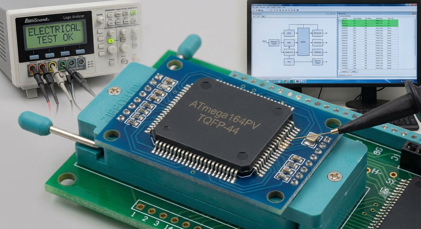
Break Microcontroller ATmega164PV Code
The ATmega164PV microcontroller has been widely adopted in long-life electronic products that require stable performance, efficient power usage, and dependable control capability. This device is commonly integrated into industrial automation equipment, smart control modules, instrumentation platforms, medical electronics, communication interfaces, environmental monitoring devices, and consumer products. Its architecture supports flexible embedded application development while storing operational firmware, configuration data, and application program functions within internal flash, eeprom, and non-volatile memory resources. In many commercial deployments, manufacturers implement protective, protected, locked, secured, or encrypted configurations to preserve proprietary design assets and reduce unauthorized duplication. As products age and original development records become unavailable, recovering historical binary, heximal, source code, or archived engineering files becomes increasingly important for maintenance and lifecycle continuity.
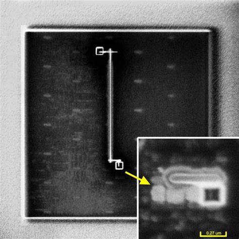
The frequency ranges are preliminary values. Actual values are TBD.
This option should not be used with crystals, only with ceramic resonators.
Our “Break Microcontroller ATmega164PV Code” service is designed for authorized recovery and reconstruction of valuable engineering assets from existing embedded hardware. The objective is not to compromise active products but to help customers retrieve historical firmware, reconstruct lost program structures, and preserve inaccessible technical documentation. Through structured laboratory workflows and device evaluation processes, our team supports projects involving memory assessment, data recovery, and high-level decode of historical firmware structures.
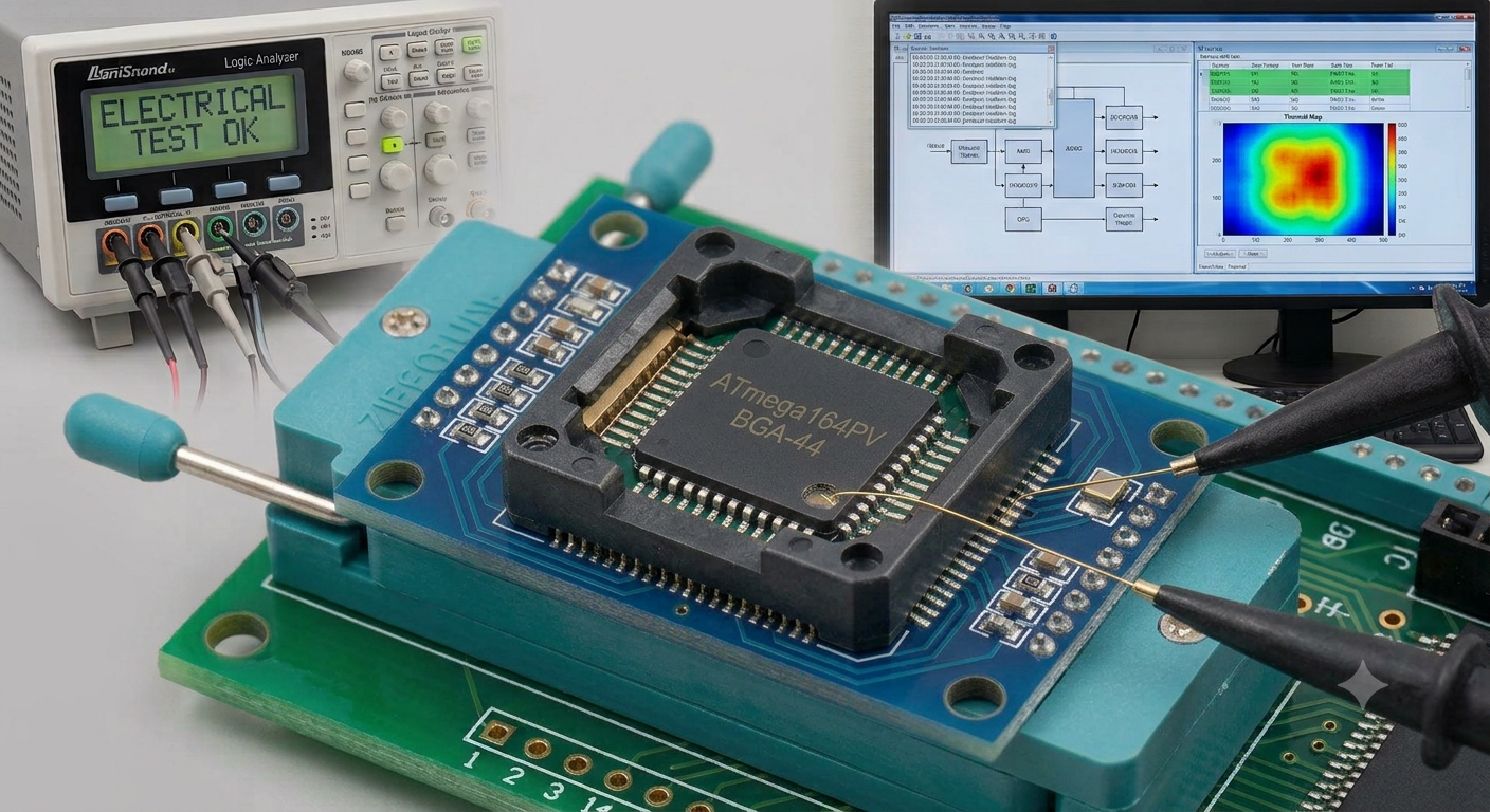
Depending on project scope and authorization, controlled inspection methods may be used to evaluate storage organization and recover available binary and heximal records from internal flash and eeprom regions. Extracted information is reorganized into engineering-ready file and archive outputs that assist customers in maintaining legacy systems, preparing controlled clone references, validating compatibility, or supporting limited duplicate production programs.
These options are intended for use with ceramic resonators and will ensure frequency stability at start-up. They can also be used with crystals when not operating close to the maximum frequency of the device, and if frequency stability at start-up is not important for the application.
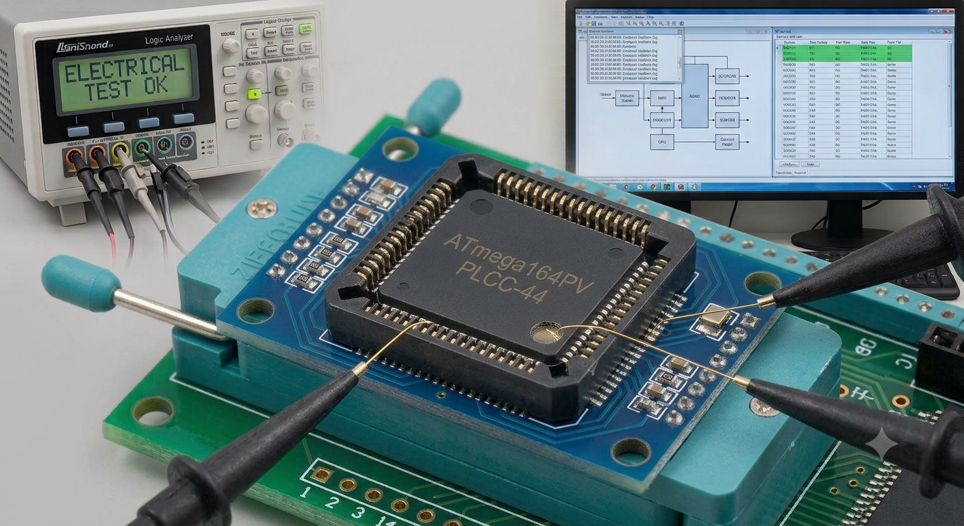
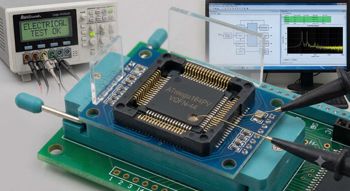
The technical workflow combines preservation methodology with disciplined engineering analysis. Device behavior is documented and internal structures are evaluated to reconstruct meaningful source code references and recover operational firmware relationships. Specialized analysis may support interpretation of archived data and reconstruction of historical program logic while preserving consistency with the original hardware environment. Where appropriate and legally authorized, controlled package examination and limited decapsulate procedures may assist interpretation of inaccessible memory structures and organization of recovered binary files. Rather than attempting to attack, break, or hack active security controls, the process prioritizes controlled recovery, validation, and documentation of engineering assets. Structured decode procedures help transform fragmented archives into usable outputs that support product continuity and long-term technical management.
This Crystal Oscillator is a full swing oscillator, with rail-to-rail swing on the XTAL2 output. This is useful for driving other clock inputs and in noisy environments. The current consumption is higher than the “Low Power Crystal Oscillator” on page 41. Note that the Full Swing Crystal Oscillator will only operate for Vcc = 2.7 – 5.5 volts.
C1 and C2 should always be equal for both crystals and resonators. The optimal value of the capacitors depends on the crystal or resonator in use, the amount of stray capacitance, and the electromagnetic noise of the environment. Some initial guidelines for choosing capacitors for use with crystals are given in Table 12. For ceramic resonators, the capacitor values given by the manufacturer should be used.
If 8 MHz frequency exceeds the specification of the device (depends on VCC), the CKDIV8 Fuse can be programmed in order to divide the internal frequency by 8. It must be ensured that the resulting divided clock meets the frequency specification of the device. These options should only be used when not operating close to the maximum frequency of the device, and only if frequency stability at start-up is not important for the application. These options are not suitable for crystals. These options are intended for use with ceramic resonators and will ensure frequency stability at start-up. They can also be used with crystals when not operating close to the maximum frequency of the device, and if frequency stability at start-up is not important for the application.
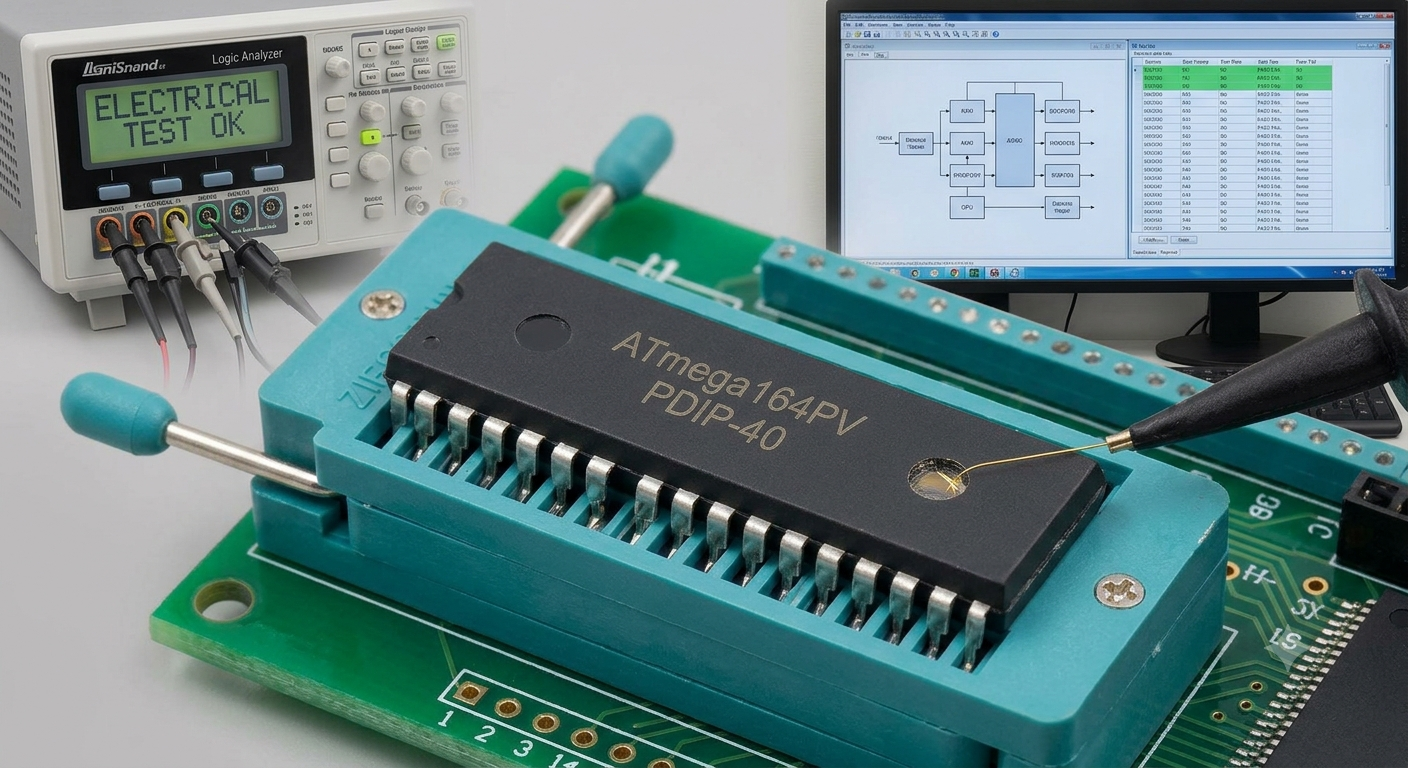
For end users, recovering ATmega164PV code can significantly reduce redevelopment effort and preserve proven designs already deployed in the field. Access to historical firmware, organized data archives, and reconstructed source code enables maintenance teams to support existing installations, modernize platforms, and extend product service life. Engineering groups can reuse validated program behavior, document historical architecture, and maintain operational compatibility without restarting development from the beginning. By combining embedded expertise with responsible recovery practices, our service helps customers transform inaccessible device content into reusable engineering knowledge and maintain continuity across critical electronic systems.
Reverse Engineering IC ATmega164V Code
Reverse Engineering IC ATmega164V Code and extract MCU ATmega164V heximal from embedded program memory and data memory, clone ATmega164V code to new microcontroller.
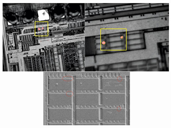
The device is shipped with internal RC oscillator at 8.0MHz and with the fuse CKDIV8 programmed, resulting in 1.0MHz system clock. The startup time is set to maximum and time-out period enabled.
(CKSEL = “0010”, SUT = “10”, CKDIV8 = “0”). The default setting ensures that all users can make their desired clock source setting using any available programming interface if Recover IC STM32F107RCT6 code.
Any clock source needs a sufficient VCC to start oscillating and a minimum number of oscillating cycles before it can be considered stable.
To ensure sufficient VCC, the device issues an internal reset with a time-out delay (tTOUT) after the device reset is released by all other reset sources. “On-chip Debug System” on page 56 describes the start conditions for the internal reset if copy microcontroller PIC16F684 firmware.
The delay (tTOUT) is timed from the Watchdog Oscillator and the number of cycles in the delay is set by the SUTx and CKSELx fuse bits. The selectable delays are shown in Table 8. The frequency of the Watchdog Oscillator is voltage dependent as shown in “ATmega164 Typical Characteristics – Preliminary Data”.
Main purpose of the delay is to keep the AVR in reset until it is supplied with minimum Vcc. The delay will not monitor the actual voltage and it will be required to select a delay longer than the Vcc rise time. If this is not possible, an internal or external Brown-Out Detection circuit should be used after Recover chip pic16f913 binary.
A BOD circuit will ensure sufficient Vcc before it releases the reset, and the time-out delay can be disabled. Disabling the time-out delay without utilizing a Brown-Out Detection circuit is not recommended.
The oscillator is required to oscillate for a minimum number of cycles before the clock is considered stable. An internal ripple counter monitors the oscillator output clock, and keeps the internal reset active for a given number of clock cycles. The reset is then released and the device will start to execute.
The recommended oscillator start-up time is dependent on the clock type, and varies from 6 cycles for an externally applied clock to 32K cycles for a low frequency crystal.
The start-up sequence for the clock includes both the time-out delay and the start-up time when the device starts up from reset. When starting up from Power-save or Power down mode, Vcc is assumed to be at a sufficient level and only the start-up time is included.
Pins XTAL1 and XTAL2 are input and output, respectively, of an inverting amplifier which can be configured for use as an On-chip Oscillator, as shown in Figure 22. Either a quartz crystal or a ceramic resonator may be used.
This Crystal Oscillator is a low power oscillator, with reduced voltage swing on the XTAL2 output. It gives the lowest power consumption, but is not capable of driving other clock inputs, and may be more susceptible to noise in noisy environments. In these cases, refer to the “Full Swing Crystal Oscillator” on page 43.
C1 and C2 should always be equal for both crystals and resonators. The optimal value of the capacitors depends on the crystal or resonator in use, the amount of stray capacitance, and the electromagnetic noise of the environment. Some initial guidelines for choosing capacitors for use with crystals are given in Table 9. For ceramic resonators, the capacitor values given by the manufacturer should be used.
Posted in Recover Chip |
Tags: reverse engineering ic protected archive, reverse engineering ic protected bin, reverse engineering ic protected code, reverse engineering IC protected content, reverse engineering IC protected data, reverse engineering ic protected eeprom, reverse engineering IC protected file, reverse engineering ic protected firmware, reverse engineering ic protected hex, reverse engineering ic protected information, reverse engineering ic protected memory, reverse engineering ic protected program |
Comments Closed