 Extract Wiring Diagram from Existing Circuit Board
 July 31st, 2012 |
 Author:
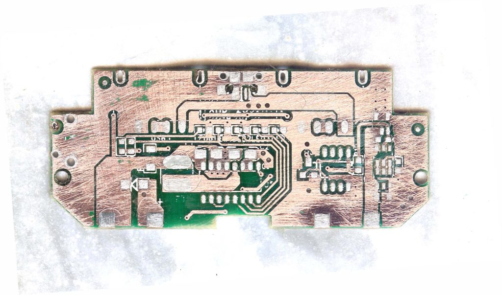
Extract Wiring Diagram from Existing Circuit Board is able to help engineer to reproduce the printed circuit board which hasn’t been produced for a long time;
Checking and Optimization:
Whole process of extract wiring diagram from circuit board finish only after checking and testing done and approve pass, for nominal value of those distribution parameter sensitive components of circuit board need to check and optimizing, according to circuit board design, compare the extracted wiring diagram with circuit board design file to ensure the accuracy and completeness.
Extract Circuit Diagram from Existing PCB Board
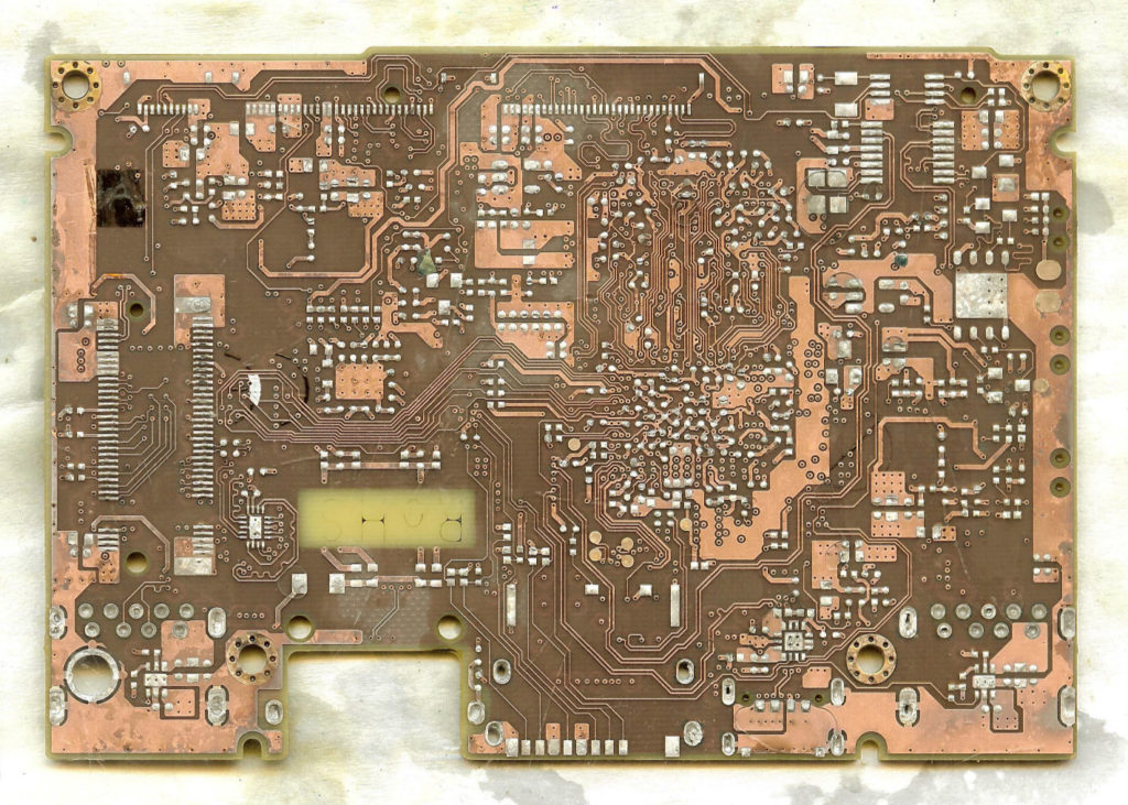
Extract Circuit Diagram from Existing PCB Board and use these documents for PCB reproduction, circuit diagram normally include layout drawing, Gerber file, BOM list and schematic;
Master the basic framework, take the similar PCB Board as reference when extract circuit board wiring diagram:
For those basic formats of electronic PCB Board circuit diagram drawing, engineer should understand them very thoroughly, because they can help to draw some simple and typical circuit unit directly, but also form electronic circuit framework.
From other side, please remember that same kind of electronic product can be similar to a certain extent, engineer should accumulate more experience and can take them as reference to restore schematic diagram from printed circuit board.
 Posted in PCB Clone |
 Tags: extract circuit diagram, extract circuit schematic, extract schematic diagram, Extract wiring diagram, extract wiring schematic |
 Comments Closed
Identify the circuit board track layout
Identify the circuit board track pattern dissipation and layout circuit board track pattern logically:
For distinguish of ground plane, power supply circuit and signal circuit, also require engineer to have related power supply, circuit connection, circuit board layout and PCB Reverse Engineering knowledge. How to distinguish these different kinds of circuit can rely on component connection situation, copper thickness and feature of electronic product.
During the process of PCB layout & PCB Clone, in order to avoid the cross line, large bulks of ground signal can be applied on the ground plane, different circuit can use different colors to help distinguish one another, also specified symbol can use on specified components, can even separate unit circuit and draw them. And finally can integrate them together.
Extract schematic diagram from Existing PWB
Orient the RIGHT part:
This right part as a standard one can be viewed as the main part before the PWB schematic diagram being extracted, according to these standard part’s lead can to great extend ensure the accuracy of schematic diagram extraction of PWB.
In view of engineer, it isn’t too much trouble for them to locate standard part, generally, they can choose those parts which play the main role in the functional module, they usually have more leads and bigger size which could be helpful for drawing, such as integrate circuit, transformer and crystal.
Reverse Engineering Circuit Diagram from Existing PCB Card
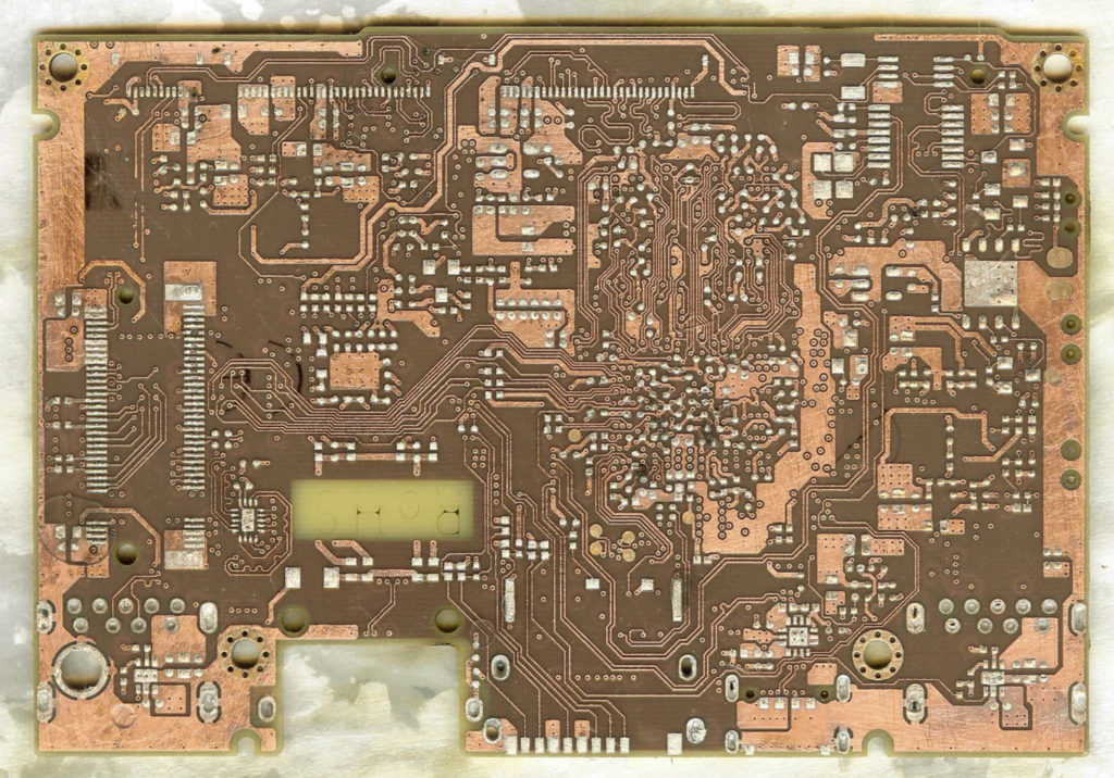
Reverse Engineering Circuit Diagram from Existing PCB Card will help designer to re-manufacture the circuit board according to restored schematic diagram.
Carve out different zones according to functions:
During the process of reverse engineering PCB board wiring diagram, carve up different zones according to module function can greatly help engineers to avoid some unnecessary troubles, improve efficiency of drawing. Generally speaking, the components of PCB card which work for same functions can be centralized, which can bring more convenience evidence.
However, carve up functional module isn’t at random. It requires engineers to have better knowledge of printed circuit board layout optimization project.
First of all, find out the core part of the single functional unit, and then through this core part can find out other components, finally form a function subarea. Establishment of function subarea is the basement of PCB card circuit diagram compilation. Additional, during this process, those designators of components in sequence can also help you locate the function subarea sooner.
PCB Redesign
The Problem why the PCB Redesign occurs is because the original Printed circuit board layout drawing and gerber file need to be modified which can be fulfilled by extract wiring diagram of circuit board;
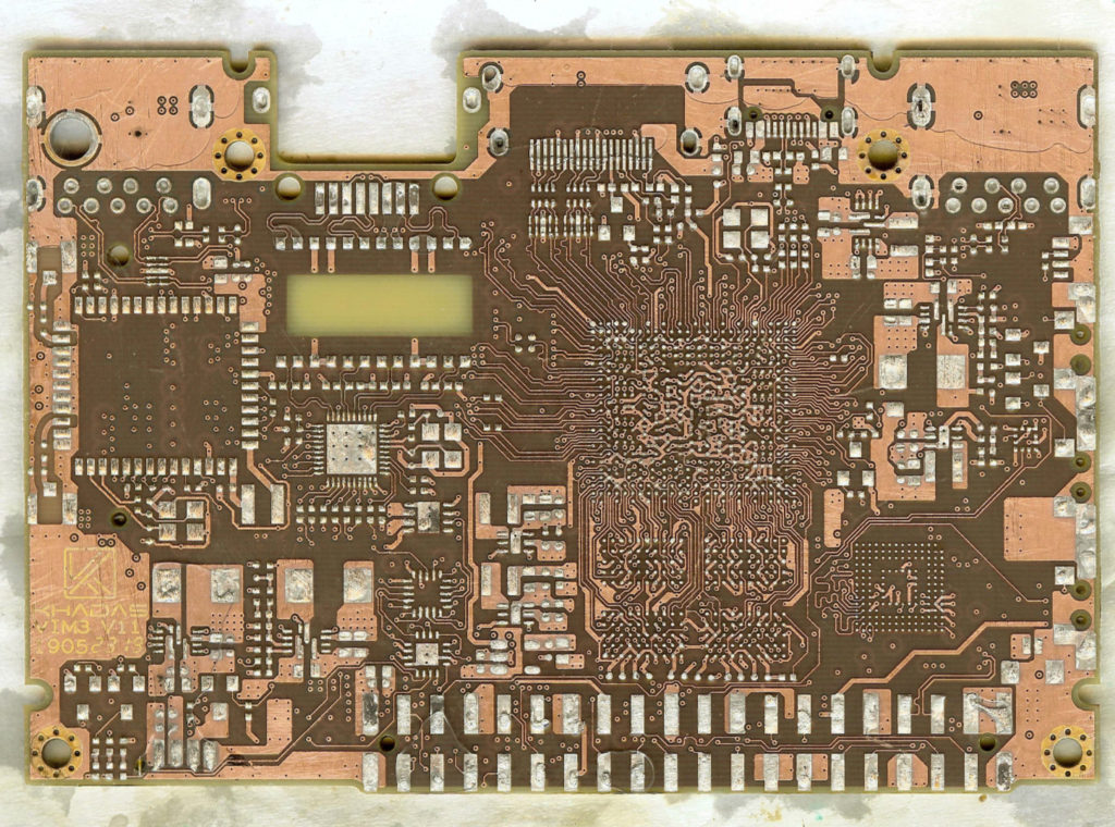
Do you have legacy circuit board layouts that were created with an obsolete CAD system? Many times these layouts are still being used to maintain current products or as replacement parts for older products. Do you frequently have to redesign PCB board layouts for a better emc performance? Do you have to transfer these layouts from one manufacturing platform to another? Are you looking at a complete PCB drawing recreation to facilitate this?
The Solution which PCB Redesign can bring:
As an alternate solution to PCB reverse engineering or Gerber modification is to “Reverse Engineering” the Gerber files into an intelligent format that can be read by today’s PCB CAD systems. This process takes the Gerber artwork, builds intelligence and electrical nets and ends in a complete CAD database which ensures a pefect match with the original circuit layout.
Posted in PCB Clone |
Tags: circuit board redesign, circuit card redesign, double side pcb redesign, pcb board redesign, pcb card redesign, pcb plate redesign, pcb redesign, pcba redesign, printed circuit board redesign, pwb redesign |
Comments Closed
Recovery Chip PIC16F506 Firmware
Recovery Chip PIC16F506 Firmware from microcontroller memory, crack PIC16F506 MCU flash and eeprom to readout PIC16F506 MCU code;
Random recovery operations allow the master to access any memory location in a random manner. To perform this type of recovery operation, first the word address must be set. This is done by sending the word address to the device as part of a write operation.
What sets a microcontroller apart from other processors are special circuits to deal with the needs of real-time applications. The PIC16F506 family of microcontrollers has a host of such features intended to maximize system reliability, minimize cost through elimination of external components, provide power saving operating modes and offer code protection when Reverse engineering Chip pic18f248 binary firmware.
These features are:
Oscillator selection
Reset
– Power-On Reset (POR)
– Device Reset Timer (DRT)
– Wake-up from SLEEP on pin change
Watchdog Timer (WDT)
SLEEP
Code protection
ID locations
In-circuit Serial Programming
The PIC16F506 has a Watchdog Timer which can be shut off only through configuration bit WDTE. It runs off of its own RC oscillator for added reliability.
If using XT or LP selectable oscillator options, there is always an 18 ms (nominal) delay provided by the Device Reset Timer (DRT), intended to keep the chip in reset until the crystal oscillator is stable.
If using INTRC or EXTRC there is an 18 ms delay only on VDD power-up. With this timer on-chip, most applications need no external reset circuitry.
The SLEEP mode is designed to offer a very low current power-down mode. The user can wake-up from SLEEP through a change on input pins or through a Watchdog Timer time-out. Several oscillator options are also made available to allow the part to fit the application, including an internal 4 MHz oscillator. The EXTRC oscillator option saves system cost while the LP crystal option saves power.
A set of configuration bits are used to select various options. The PIC16F506 configuration word consists of 12 bits. Configuration bits can be programmed to select various device configurations. Two bits are for the selection of the oscillator type, one bit is the Watchdog Timer enable bit, and one bit is the MCLR enable bit.
Posted in Recover Chip |
Tags: recover protected chip bin, recover protected chip data, recover protected chip eeprom, recover protected chip file, recover protected chip firmware, recover protected chip flash, recover protected chip hex, recover protected chip memory, recover protected chip program, recover protected chip software |
Comments Closed
Introduction of Flexible Circuit Assembly
Flexible circuits offer some unique challenges to the assembly process. The assembly materials and processes for populating and interconnecting components to a flexible circuit range are essentially identical to those used for standard rigid or rigid flex pcb, but there are some twists required, as will be shown. The assembly processes range from very simple methods, such as manual component insertion and hand soldering (which requires little or no fixturing), to fully automated methods, which normally require specially developed, design-specific and dedicated fixtures.
How, then, does one choose an assembly process and method for flexible circuits? To begin appropriately, it is necessary to consider a number of important factors: What is the flexible circuit base material? What types of components will be used? How many assemblies will be built? These and other important questions must be addressed before one can adequately make the proper decisions regarding assembly. These seemingly simple matters can greatly influence the pcb assembly choice. For example, it is commonly assumed that polyester circuits cannot be used in applications where soldering is required. The reason for this assumption is that polyester films have a low melt point and will be grossly distorted by the tin-lead soldering process. However, when properly fixtured, soldering can be used for joining components to polyester. A number of major OEMs have been doing just that for many years. They have developed methods that provide proper shielding of the body of the polyester circuit in process. The distortion of the material can be localized to areas adjacent to the point of connection.
With the advent of the well-meant but misguided legislation mandating the use of lead-free solders, there will be significant challenges ahead, as lead-free solders have a roughly 30-40ºC higher melting temperature than traditional tin-lead solders. Sadly, it appears that traditional tin-lead solders are actually more environmentally friendly, so the law does double damage. One alternative is to use lower-temperature solders, or conductive adhesives can also be employed. The important thing is that manufacturers not limit themselves in their thinking and that they be open to alternative solutions. Following is a brief review of the key elements of flex circuit assembly.
PCB Circuit Board Electronics
Interconnect technology is expanding to include printed systems. As detailed in the iNEMI Organic and Printed Electronics Roadmap, there is a bounty of printed electronics technologies, such as “drop on demand,” Xerography, micropen, et al. It is not within the scope of this chapter to detail the principles, advantages, benefits, etc., of each technology; rather, it’s important for electronic packaging and interconnect designers to understand the salient features of printed electronics and digital fabrication technologies as well as the similarities and differences among conventional printed circuit technologies and processes.
Digital fabrication can be viewed as the creation of electro-optical-mechanical-thermal systems by means of either parallel or sequential additive processes, as controlled by a digital device. As with any technology, the designer should consider and take advantage of the technology’s features before applying it. In the case of digital fabrication, those features include adaptive, additive, roll-to-roll processes and the ability to fabricate on curved, conformal, curvilinear surfaces.
Most often, digital fabrication is accomplished in a roll-to-roll process, but panel-based digital fabrication is also possible. The revolutionary aspect of digital fabrication, as compared to conventional printed circuit board, is the ability to simultaneously create electronic and/or optical devices, electrical interconnects, mechanical structures, and thermal management systems. For example, using conventional technology and processes, a television remote control is produced by packaging and assembling tens to hundreds of electronic devices onto PCBs and subsequently assembling the PCBs, interconnect, LED, touchpad, etc., within a plastic housing. Digital fabrication would allow the entire system to be fabricated, layer-by-layer, in a fashion similar to that of stereolithography apparatus (SLA). Applying digital fabrication requires a transformation in thinking by electronic system designers: digital fabrication provides for the 2D and 3D design and fabrication of systems that are not limited to electrical interconnect and passive devices.
In digital fabrication, materials with the necessary electrical, mechanical, thermal, and optical properties to form the desired devices, systems, etc., are deposited onto a substrate. Polymer and plastic are the most common substrate materials, due to their compatibility with low-cost, high-through-put processing. However, rigid substrates can be used as well. The materials used in forming electronic devices and interconnect are, typically, conductive inks and dielectrics. Any material, however, that can be dispensed by the dispensing system (“print head” plus material control) can be used. The materials used in forming mechanical and thermal structures, likewise, are defined by the application and limited by the capabilities of the “print head” and material control system. To date, biological, organic, optical, and many types of functional materials have been printed.
Given that devices and structures are being “built-up,” layer-by-layer, there are key differences in the resulting device and feature attributes. For example, vias can be formed as filled or partially filled and can be conductive and/or nonconductive, electrically and/or thermally. Unlike conventional pcb circuit board technology and processes, digital fabrication can be used to produce vias of any geometry. Similarly, individual traces can be of any geometry and can be produced to effect sidewalls with attributes to support application needs. Conductors produced using conventional pcb manufacture technology have sidewalls that are tapered or orthogonal. Digital fabrication could be used to produce conductors with irregular sidewall features, as related to specific performance or mechanical applications. Furthermore, in digital fabrication, mechanical, thermal, and other features could be included in the construction of conductors.
Currently, the primary applications for printed electronics are OLEDs, and RFID. Photovoltaics are also an application for printed electronics, but this field is immature compared to OLEDs and RFID.
Transistors that operate in the tens of megahertz have been printed; recently, researchers at the University of Illinois (Rogers et al.) announced that they had printed silicon circuits on plastic that operate at switching speeds of 500 megahertz. As shown in Figure 27, there are demands for printed, stable, high-speed digital and high-fidelity analog devices; however, materials to produce devices other than low-speed, simple ones are lacking. Accordingly, other than novel devices produced in laboratories, printed electronics have not been used to produce the basic “building-block” high-speed digital or analog devices (e.g., FPGAs and operational amplifiers, respectively). These components are fundamental to systems comprised of analog devices.
Similarly, with respect to printing electrical interconnects, digital fabrication is in its infancy. Plated vias, a staple of the layer-to-layer interconnect found in conventional pcb circuit board technology, are nonexistent or crudely implemented in digital fabrication. Moreover, the electrical performance and reliability of vias and conductors are either not known or, with respect to characterization, known incompletely. It will be interesting to observe if and when the creation and maintenance of electronic and interconnect standards are realized.
Decrypt IC PIC16F505 Flash
Decrypt IC PIC16F505 Flash memory content, and then extract chip PIC16F505 code out and decode PIC16F505 mcu embedded firmware;
Since the device will not acknowledge during a write cycle, this can be used to determine when the cycle is complete (this feature can be used to maximize bus throughput).
Once the stop condition for a write command has been issued from the master, the device initiates the internally timed write cycle. ACK polling can be initiated immediately if break microcontroller pic12f617 binary.
This involves the master sending a start condition followed by the control byte for a write command (R/W = 0). If the device is still busy with the write cycle, then no ACK will be returned.
If no ACK is returned, then the start bit and control byte must be re-sent. If the cycle is complete, then the device will return the ACK and the master can then proceed with the next read or write command. See Figure 7-6 for flow diagram after break IC pic12hv615 heximal.
It contains an address counter that maintains the address of the last word accessed, internally incremented by one. Therefore, if the previous read access was to address n, the next current address read operation would access data from address n + 1.
Upon receipt of the slave address with the R/W bit set to one, the device issues an acknowledge and transmits the eight bit data word. The master will not acknowledge the transfer but does generate a stop condition and the device discontinues transmission.
Read operations are initiated in the same way as write operations with the exception that the R/W bit of the slave address is set to one. There are three basic types of read operations: current address read, random read and sequential read before recover mcu pic16hv616 eeprom.