 Restore Circuit Diagram from existing PCB Card
All the PCB card circuit diagrams we have restored are all proofreading by pcb card pattern network, all the component’s designation, part number and network name are all complete and easy to check. Also apply “relative centralization of components of functional module” onto module drawing method, it is readability can even equal to original designed circuit diagram after restoration. Customer can easily understand the original design idea of product, to capture some flash spot of high advanced design, moreover, customer’s unique idea can be integrate into it for launch the high advanced product after restore circuit diagram from pcb card service.
Restore Schematic Diagram from Existing Circuit Board
Restore Schematic Diagram from Existing Circuit Board can play an important effect when repairing printed circuit board in the absence of schematic diagram or related technical drawings from original Manufacturer;
Either analyzing Circuit Board principle and electronic product feature through PCB Card cloning, or as basement and technical support for Circuit Board design after PCB Restoration, extract wiring diagram from circuit board plays a very special role. Furthermore, it can also take an important effect during the process of product adjustment, repair and modification, restore schematic diagram from circuit board is critical part of our service catalogue. You just need to provide sample circuit board prototype, or circuit board layout file, we can recover schematic diagram from circuit board with 100% accuracy.
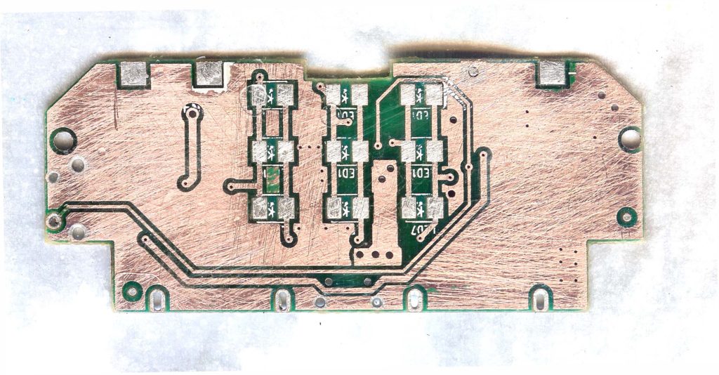
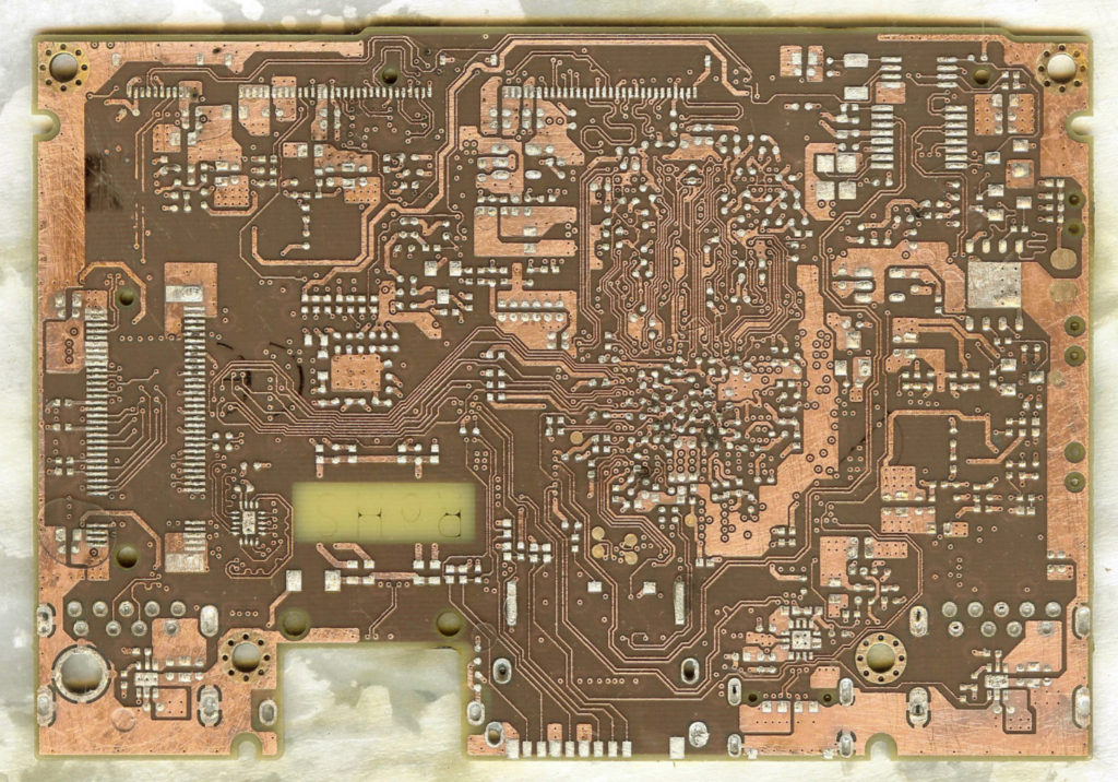
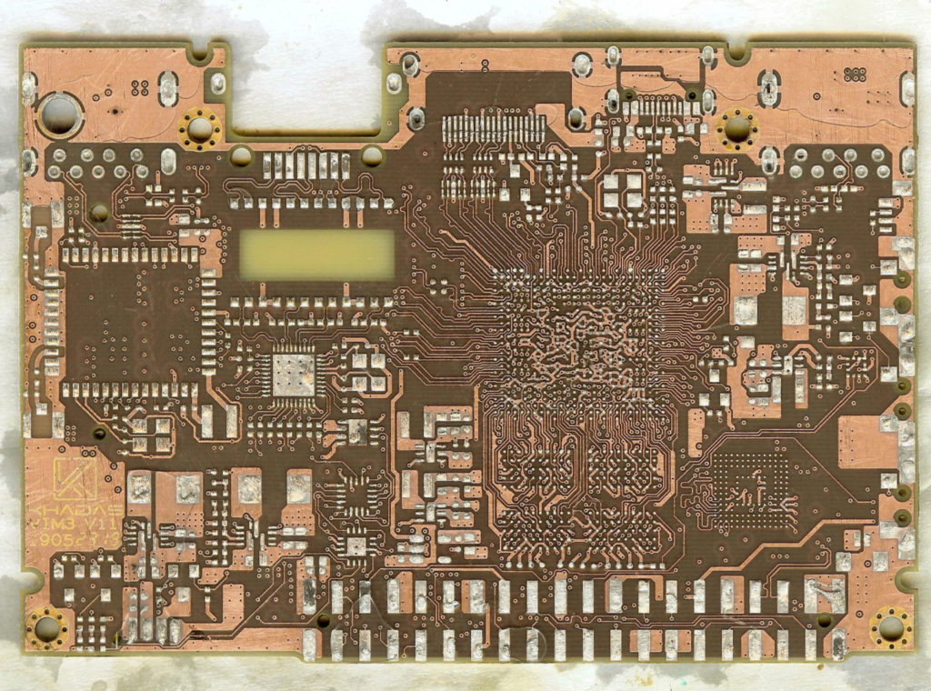
Reverse Engineering Wiring Diagram from existing PCB Board
Reverse Engineering Wiring Diagram from existing PCB Board starts from desolder all the electronic parts off the circuit card, as well as stripping off the solder resist mask over the top and bottom layer;
In the research of restoring schematic diagram from existing PCB Board, definition of Recreating existing PCB Board is regenerate PCB wiring diagram through PCB Board pattern file or directly draw it according to physical electronic PCB Board sample under the purpose of description of PCB Board principle and working environment.
Moreover, this wiring diagram from PCB Reverse engineering can also being used to analyze functional feature of electronic product.
Extract Wiring Diagram from Existing Circuit Board
Extract Wiring Diagram from Existing Circuit Board is able to help engineer to reproduce the printed circuit board which hasn’t been produced for a long time;
Checking and Optimization:
Whole process of extract wiring diagram from circuit board finish only after checking and testing done and approve pass, for nominal value of those distribution parameter sensitive components of circuit board need to check and optimizing, according to circuit board design, compare the extracted wiring diagram with circuit board design file to ensure the accuracy and completeness.
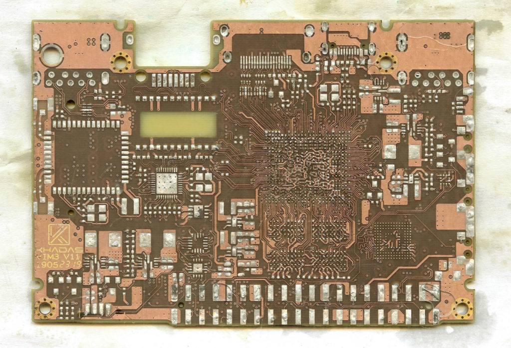
Extract Circuit Diagram from Existing PCB Board
Extract Circuit Diagram from Existing PCB Board and use these documents for PCB reproduction, circuit diagram normally include layout drawing, Gerber file, BOM list and schematic;
Master the basic framework, take the similar PCB Board as reference when extract circuit board wiring diagram:
For those basic formats of electronic PCB Board circuit diagram drawing, engineer should understand them very thoroughly, because they can help to draw some simple and typical circuit unit directly, but also form electronic circuit framework.
From other side, please remember that same kind of electronic product can be similar to a certain extent, engineer should accumulate more experience and can take them as reference to restore schematic diagram from printed circuit board.
Identify the circuit board track layout
Identify the circuit board track pattern dissipation and layout circuit board track pattern logically:
For distinguish of ground plane, power supply circuit and signal circuit, also require engineer to have related power supply, circuit connection, circuit board layout and PCB Reverse Engineering knowledge. How to distinguish these different kinds of circuit can rely on component connection situation, copper thickness and feature of electronic product.
During the process of PCB layout & PCB Clone, in order to avoid the cross line, large bulks of ground signal can be applied on the ground plane, different circuit can use different colors to help distinguish one another, also specified symbol can use on specified components, can even separate unit circuit and draw them. And finally can integrate them together.
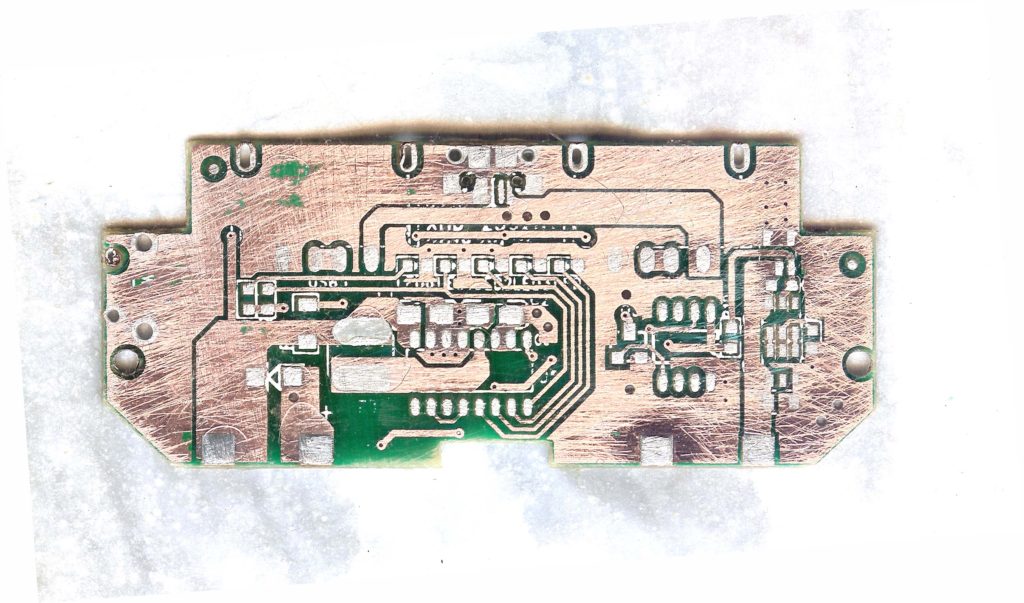
Extract schematic diagram from Existing PWB
Orient the RIGHT part:
This right part as a standard one can be viewed as the main part before the PWB schematic diagram being extracted, according to these standard part’s lead can to great extend ensure the accuracy of schematic diagram extraction of PWB.
In view of engineer, it isn’t too much trouble for them to locate standard part, generally, they can choose those parts which play the main role in the functional module, they usually have more leads and bigger size which could be helpful for drawing, such as integrate circuit, transformer and crystal.
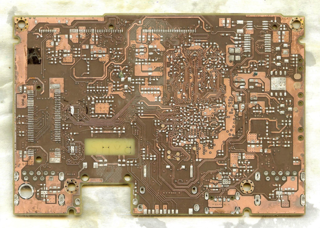
Reverse Engineering Circuit Diagram from Existing PCB Card
Reverse Engineering Circuit Diagram from Existing PCB Card will help designer to re-manufacture the circuit board according to restored schematic diagram.
Carve out different zones according to functions:
During the process of reverse engineering PCB board wiring diagram, carve up different zones according to module function can greatly help engineers to avoid some unnecessary troubles, improve efficiency of drawing. Generally speaking, the components of PCB card which work for same functions can be centralized, which can bring more convenience evidence.
However, carve up functional module isn’t at random. It requires engineers to have better knowledge of printed circuit board layout optimization project.
First of all, find out the core part of the single functional unit, and then through this core part can find out other components, finally form a function subarea. Establishment of function subarea is the basement of PCB card circuit diagram compilation. Additional, during this process, those designators of components in sequence can also help you locate the function subarea sooner.
PCB Redesign
The Problem why the PCB Redesign occurs is because the original Printed circuit board layout drawing and gerber file need to be modified which can be fulfilled by extract wiring diagram of circuit board;
Do you have legacy circuit board layouts that were created with an obsolete CAD system? Many times these layouts are still being used to maintain current products or as replacement parts for older products. Do you frequently have to redesign PCB board layouts for a better emc performance? Do you have to transfer these layouts from one manufacturing platform to another? Are you looking at a complete PCB drawing recreation to facilitate this?
The Solution which PCB Redesign can bring:
As an alternate solution to PCB reverse engineering or Gerber modification is to “Reverse Engineering” the Gerber files into an intelligent format that can be read by today’s PCB CAD systems. This process takes the Gerber artwork, builds intelligence and electrical nets and ends in a complete CAD database which ensures a pefect match with the original circuit layout.
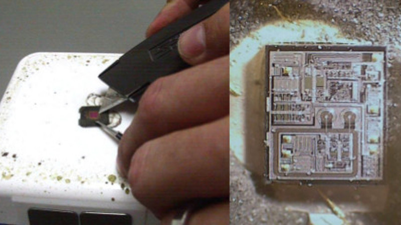
Recovery Chip PIC16F506 Firmware
Recovery Chip PIC16F506 Firmware from microcontroller memory, crack PIC16F506 MCU flash and eeprom to readout PIC16F506 MCU code;
Random recovery operations allow the master to access any memory location in a random manner. To perform this type of recovery operation, first the word address must be set. This is done by sending the word address to the device as part of a write operation.
What sets a microcontroller apart from other processors are special circuits to deal with the needs of real-time applications. The PIC16F506 family of microcontrollers has a host of such features intended to maximize system reliability, minimize cost through elimination of external components, provide power saving operating modes and offer code protection when Reverse engineering Chip pic18f248 binary firmware.
These features are:
Oscillator selection
Reset
– Power-On Reset (POR)
– Device Reset Timer (DRT)
– Wake-up from SLEEP on pin change
Watchdog Timer (WDT)
SLEEP
Code protection
ID locations
In-circuit Serial Programming
The PIC16F506 has a Watchdog Timer which can be shut off only through configuration bit WDTE. It runs off of its own RC oscillator for added reliability.
If using XT or LP selectable oscillator options, there is always an 18 ms (nominal) delay provided by the Device Reset Timer (DRT), intended to keep the chip in reset until the crystal oscillator is stable.
If using INTRC or EXTRC there is an 18 ms delay only on VDD power-up. With this timer on-chip, most applications need no external reset circuitry.
The SLEEP mode is designed to offer a very low current power-down mode. The user can wake-up from SLEEP through a change on input pins or through a Watchdog Timer time-out. Several oscillator options are also made available to allow the part to fit the application, including an internal 4 MHz oscillator. The EXTRC oscillator option saves system cost while the LP crystal option saves power.
A set of configuration bits are used to select various options. The PIC16F506 configuration word consists of 12 bits. Configuration bits can be programmed to select various device configurations. Two bits are for the selection of the oscillator type, one bit is the Watchdog Timer enable bit, and one bit is the MCLR enable bit.