Archive for the ‘PCB Clone’ Category
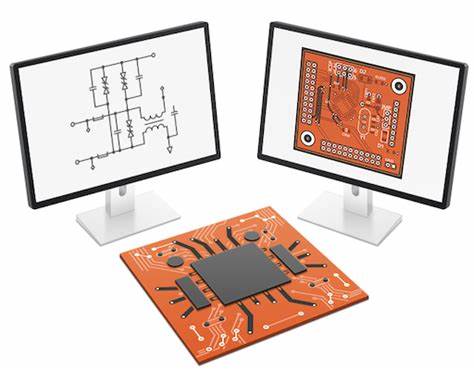
 Extract Circuit Diagram from Existing PCB Board
Extract Circuit Diagram from Existing PCB Board and use these documents for PCB reproduction, circuit diagram normally include layout drawing, Gerber file, BOM list and schematic;
Master the basic framework, take the similar PCB Board as reference when extract circuit board wiring diagram:
For those basic formats of electronic PCB Board circuit diagram drawing, engineer should understand them very thoroughly, because they can help to draw some simple and typical circuit unit directly, but also form electronic circuit framework.
From other side, please remember that same kind of electronic product can be similar to a certain extent, engineer should accumulate more experience and can take them as reference to restore schematic diagram from printed circuit board.
Extract schematic diagram from Existing PWB
Orient the RIGHT part:
This right part as a standard one can be viewed as the main part before the PWB schematic diagram being extracted, according to these standard part’s lead can to great extend ensure the accuracy of schematic diagram extraction of PWB.
In view of engineer, it isn’t too much trouble for them to locate standard part, generally, they can choose those parts which play the main role in the functional module, they usually have more leads and bigger size which could be helpful for drawing, such as integrate circuit, transformer and crystal.
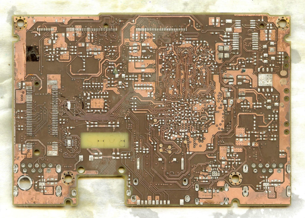
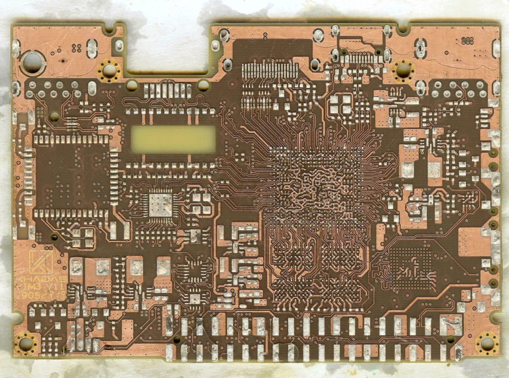
Reverse Engineering Circuit Diagram from Existing PCB Card
Reverse Engineering Circuit Diagram from Existing PCB Card will help designer to re-manufacture the circuit board according to restored schematic diagram.
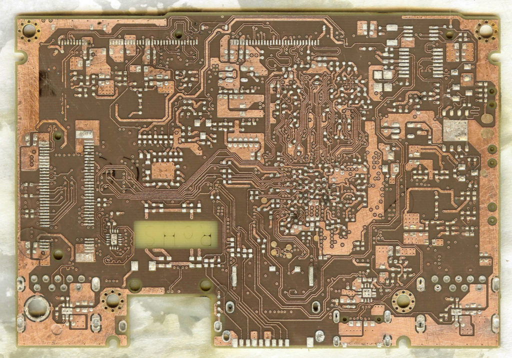
Carve out different zones according to functions:
During the process of reverse engineering PCB board wiring diagram, carve up different zones according to module function can greatly help engineers to avoid some unnecessary troubles, improve efficiency of drawing. Generally speaking, the components of PCB card which work for same functions can be centralized, which can bring more convenience evidence.
However, carve up functional module isn’t at random. It requires engineers to have better knowledge of printed circuit board layout optimization project.
First of all, find out the core part of the single functional unit, and then through this core part can find out other components, finally form a function subarea. Establishment of function subarea is the basement of PCB card circuit diagram compilation. Additional, during this process, those designators of components in sequence can also help you locate the function subarea sooner.
PCB Redesign
The Problem why the PCB Redesign occurs is because the original Printed circuit board layout drawing and gerber file need to be modified which can be fulfilled by extract wiring diagram of circuit board;
Do you have legacy circuit board layouts that were created with an obsolete CAD system? Many times these layouts are still being used to maintain current products or as replacement parts for older products. Do you frequently have to redesign PCB board layouts for a better emc performance? Do you have to transfer these layouts from one manufacturing platform to another? Are you looking at a complete PCB drawing recreation to facilitate this?
The Solution which PCB Redesign can bring:
As an alternate solution to PCB reverse engineering or Gerber modification is to “Reverse Engineering” the Gerber files into an intelligent format that can be read by today’s PCB CAD systems. This process takes the Gerber artwork, builds intelligence and electrical nets and ends in a complete CAD database which ensures a pefect match with the original circuit layout.
PCB Recreation Software Selection
How to judge if a PCB Recreation software is good or not, it is mainly depends on whether the function is complete or not, it is best to have all the work done within the software which will effectively increase the efficiency, include complete component library.
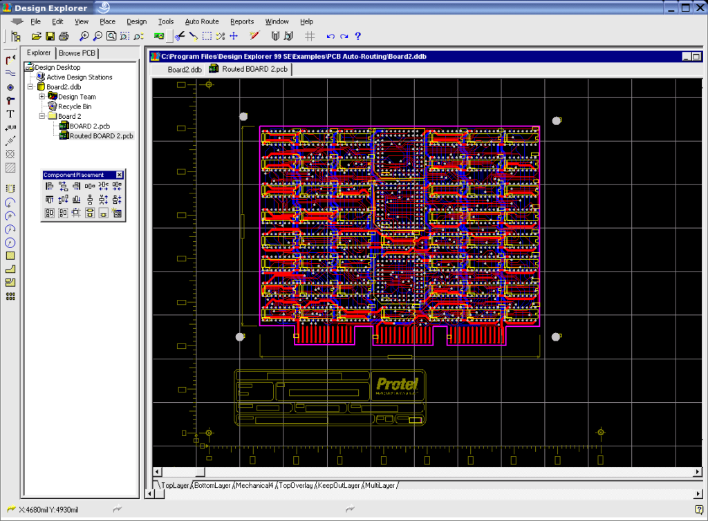
Protel 99SE can be viewed as a very outstanding one due to its component library is abundant, furthermore, it can download and upgrade the library from internel simutaneously to keep it updated consistently. This is very critical since the era of hand-drawing component when recreate circuit board has already passed, especially for those component with BGP package would cost far more than establishing library from the network automaticly.
In order to ensure the whole circuit system can be reliable and stable, designer should have large area of copper connect to POWER or GROUND layer which can decrease the impact of circuit noise and interference, so it will refers to the copper circuit network establishment issue. For a Printed Circuit board with extreme complicate network, there are lots of area need to be isolated or be connected, so we have to difine the network segment of different area and follow the principle as CONNECT SAME NETWORK segment & ISOLATE DIFFERENT NETWORK segment, just simply add copper into different network segment will cause short circuit easily.
Currently the most popular printed circuit board recreation software in the market is PROTEL 99SE, the other is QUICKPCB 2005 Ver 3.0 plus some other colorful PWB Recreation softwares. Protel 99SE is a kind of EDA design software which is applicable by operating system like WINDOW 9X/2000/NT, it has design library management system, it can instruct networking design and coordination, has very strong data exchange capabilities, and 3D model simulation capabilities, a 32-bit design software, you can complete the extracted PCB board circuit schematic design, printed circuit board design and programmable logic device design, etc., can be designed up to 32 signal layers, 16 power supply – ground layers and 16 machining layers.
The operation of QUICKPCB 2005 Ver 3.0 is in line with the majority of designers operating practices, can greatly enhance the efficiency of pcb card cloning, 1st time circuit board recreation passing rate can be further guaranteed.
Software features
Place the pads, holes, lines, arcs, vias, components, FILL, POLYGON, text;
The element attribute settings, grid settings;
Automatically capture the CTRL key element of the grid with the center;
SHIFT key to select, to select, cut, copy, delete, rotate, mirror and repeat functions;
32 level set function, Zoom;
PCB Modification Process
PCB Modification is a Process to re-edit the circuit board layout drawing, which can be converted to gerber file, and make improvement over the schematic diagram of printed circuit board after extract the schematic from it;
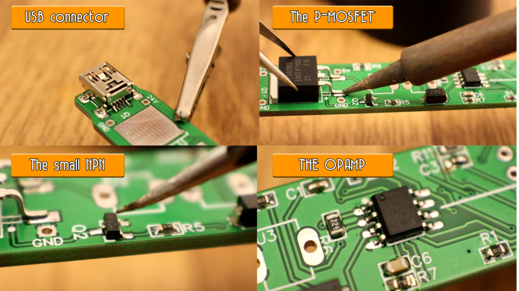
There is a 4 layer Printed Circuit Board need to being modified, all the components assembled on the surface have already been removed, PCB surface being cleaned, the process of acquire Printed circuit board gerber file for production through printed circuit board reverse engineering can be seen below:
1 Scan TOP layer circuit board, save the scanning picture and name as TOP.jpg, the DPI value can be set according to the density of PCB card, hereby we choose 400DPI as reference; Scan Bottom layer and name it as BOTTOM.jpg; Use sand paper to abrade the TOP layer copper and expose the 2nd layer copper circuit pattern, scan the circuit pattern after clean it out and name it as MID1.jpg; Use sand paper to abrade the 2nd layer copper and expose the 3nd layer copper circuit pattern, scan the circuit pattern after clean it out and name it as MID2.jpg;
2 Open PCB Board reverse engineering software, click on “file” from MAIN MENU, and then click “OPEN BMP”, select the TOP.bmp file and open it, set up DPI value and then choose the PCB Card layer feature as TOP layer, start to place components, through-hole and arrange PCB Card circuit line, after you have arranged everything on the TOP layer, save file as temporary and name as TOP-1.dpb ( save the files periodically under different name such as TOP-2, TOP-3, TOP-4 prevent files lost from unexpected power cut-off or computer breakdown );
3 Hereby comes to the final step of circuit card modification from a 4 layer circuit board.
Click on “file” from MAIN MENU, and then click “OPEN BMP”, select the BOTTOM.bmp file, at the same time open temporary file TOP-1.dpb, and you will find that circuit card TOP layer picture which has been finished already can’t align to circuit board BOTTOM layer background picture, so you have to use cursor “UP”, ”DOWN”, ”LEFT”, ”RIGHT” to move its location, now you can choose some reference points to align the layers and after you have finished alignment you can start to place components, through-hole and arrange circuit line on BOTTOM layer, what if circuit line on the TOP layer block your eyesight on BOTTOM layer? It is easy, just from the main menu “Options” select “layer color settings”, cancel the selection of TOP layer as well as silkscreen, after you have arranged everything on the BOTTOM layer, save file as temporary and name as BOTTOM-1.dpb, or as BOTTOM-1.pcb;
Repeat the process you have just been through then can output completed circuit card file from circuit card modification.
PCB Relayout Capabilities
PCB Relayout can also be defined as circuit board schematic diagram modification through which the electrical and electronic performance of printed circuit board will be improved;
—- We can handle single sided, double sided, multilayer up to 20 layers PCB Relayout;
—- No limit on nodes, holes and pads, holes refers to PCB Board with Blind & Buried via down to 0.1mm;
—- Circuit Board size range from 546*622mm due to the capability limitation, over that size;
—- No limitation on components type (through hole, surface mount, or mixed);
—- SMT pitch down to 0.2mm or less depending on board layout;
—- Application refers to Measurement, Telecommunication, Networking, Consumer Electronics, Industrial Automation;
Service Deliver:
We can send your emails containing all the information and files you need to remanufacture your electronic PCB card:
1 Schematic diagrams and drawing files; (Optional)
2 Bill of materials (BOM) list all components as well as individual description;
3 PCB plate Gerber files and drilling/outline files for the prototype or mass production;
4 Optional: A fully functional prototype PCB Assembled with all components as-specified for testing and evaluation.
PCA Reverse Engineering Introduction
PCA Reverse Engineering, also known as printed circuit board redesigning, is using clone technology onto the PCA which was designed and manufactured by others, it is to use PCB with mounted components related software to copy someone else’s PCA and then manufacture it by yourself.
This is the tradditional explanation for circuit card reverse engineering. with the PCB reverse engineering technology development, the impact and scope of this industry continues to expand rapidly, and the definition of PCB board reverse engineering also extend from the narrow sense that: PCB card clone only refers to extraction of PCB file from electronic circuit board and then restore it;
To the wide sense that pcb clone not only include PCB file extraction, Circuit Board Reverse Engineering and other related technical aspect, but also modify PCB file, the shape of the mold for electronic products, extraction of 3-dimensional model data on a variet of electronic products, compile the components list assembled on the PCA as well as individual data sheets on each component where available, decrypt microcontroller on the circuit board, crack encrypted IC on the PCB, moreover, inverse assemble the firmware of PCA Board and etc, a whole set of circuit board restoration technology.
PCB Development Accurary
Refers to the PCB Development Accurary, depends on two aspects, one is the accuracy of the software, one for the original image accuracy. Those companies who provide circuit board development service in the current market possess broad variety of precision technical capacity, and some of them have lower accuracy of PCB reverse engineering as a result of absence of high technical ability, but some of them can reach 1mil accuracy of PCB card cloning.
There is no restriction on precision if the software apply 32-bit floating point, so the most important thing depends on the accuracy of the original scanned image, for example, if with 100 million pixels, the picture can be washed 5-inch photos, but if we want it to wash into a 20-inch photos, it simply can not see, so for a high precision circuit board is, Choosing a higher DPI is necessary and critical when scaning the printed circuit board which will help to obtain an good solution pictures.
The definition of DPI is quantity of points per inch. It simply stand for the distance between two points of the scanned image is 1mil, so if DPI is 400, then the distance between two points on the image is 1000/400 = 2.5 mil, that means the accuracy is 2.5mil.
This is the most scientific measurement way, although some people claim the accurary can below 1mil, it is a prerequisite. In fact, the pcb development accurary largely depends on the original image accuracy.
To sum up, DPI value setting on the scaning machine should be determined by the requirement level of accurary of PCB board which is ready to be developped, for instance, line spacing of mobile phone circuit board usually below 1mil, then the value of DPI need to be set at more than 1000 . Scanner on the market today can satisfy this condition.
But it is hard to say the higher DPI being set, the better PCB circuitry pattern scanning job can be done.
Since higher DPI is too large to install and process in the hardware enviroment which has much higher requirement on the hardware, so the specific settings of DPI value should be adjustable according to specific pwb and their corresponding requirement. For the PCB board schematic diagram restoration with general accuracy requirement need to generally use 400DPI is enough.
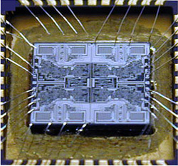
Reverse Engineering Microcontroller ATtiny85 Flash
Reverse Engineering Microcontroller ATtiny85 is able to locate the fuse bit of attiny85 then unlock the mcu attiny85 by focus ion beam, program of Flash memory will be readout directly from mcu attiny85;
Reverse Engineering Microcontroller ATtiny85 is able to locate the fuse bit of attiny85 then unlock the mcu attiny85 by focus ion beam, program of Flash memory will be readout directly from mcu attiny85
The AVR core combines a rich instruction set with 32 general purpose working registers. All the 32 registers are directly connected to the Arithmetic Logic Unit (ALU), allowing two independent registers to be accessed in one single instruction executed in one clock cycle when Recover mcu pic12ce518 bin.
The resulting architecture is more code efficient while achieving throughputs up to ten times faster than conventional CISC microcontrollers. The ATtiny24/44/84 provides the following features: 2/4/8K byte of In-System Programmable Flash, 128/256/512 bytes EEPROM, 128/256/512 bytes SRAM, 12 general purpose I/O lines, 32 general purpose working registers, a 8-bit Timer/Counter with two PWM channels, a 16-bit timer/counter with two PWM channels, Internal and External Interrupts, a 8-channel 10-bit ADC, programmable gain stage (1x, 20x) for 12 differential ADC channel pairs, a programmable Watchdog Timer with internal Oscillator, internal calibrated oscillator, and three software selectable power saving modes.
The Idle mode stops the CPU while allowing the SRAM, Timer/Counter, ADC, Analog Comparator, and Interrupt system to continue functioning. The Power-down mode saves the register contents, disabling all chip functions until the next Interrupt or Hardware Reset. The ADC Noise Reduction mode stops the CPU and all I/O modules except ADC, to minimize switching noise during ADC conversions. In Standby mode, the crystal/resonator Oscillator is running while the rest of the device is sleeping. This allows very fast start-up combined with low power consumption before Reverse engineering Microcontroller.
The device is manufactured ng Atmel’s high density non-volatile memory technology. The On-chip ISP Flash allows the Program memory to be re-programmed In-System through an SPI serial interface, by a conventional non-volatile memory programmer or by an On-chip boot code running on the AVR core. The ATtiny24/44/84 AVR is supported with a full suite of program and system development tools including: C Compilers, Macro Assemblers, Program Debugger/Simulators, In-Circuit Emulators, and Evaluation kits if Reverse engineering Microcontroller.