Archive for the ‘PCB Clone’ Category
 PCB Reverse Engineering Rationale
PCB Reverse Engineering Rationale is to extract wiring diagram from existing printed circuit board which has been out of production or not easy to get access to the new purchasing due to various reasons;
One method of controlling the high costs of replenishment spares is by pcb reverse engineering.
PCB Reverse engineering is the process of duplicating an item, functionally and dimensionally, by physically examining and measuring existing parts to develop the technical data (physical and material characteristics) required for competitive procurement.
The PCB reverse engineering process may be performed on specific items which are currently purchased sole-source. This may be due to limited data rights, in inadequate TDP, a diminished or non-existent source of supply, or as part of a Product Improvement Program (PIP).
Normally, PCB card cloning will not be cost effective unless the items under consideration are of a high dollar value or are procured in large quantities. Such items may be reverse engineered if an economical savings over their acquisition life cycle is demonstrated, and if other methods of acquiring the necessary technical data for competitive reprocurement are either more costly or not available.
Article quote from MLK-HDBK-115A(ARMY)
PCB Reverse Engineering Background in the U.S. department of Defense
PCB Reverse Engineering Background has a profound effect over the past years which is helping the engineer to restore circuit board schematic diagram from original physical samples include the gerber file, layout drawing and BOM list;
Defense contractors who supply systems, equipment and spare parts during the initial production phase of a weapon system acquisition in which they have performed in the development, frequently become the “sole-source” for follow-on procurements.
The cost of items procured under these sole source conditions are sometimes inflated beyond their true value. Consequently, procurement costs for spare parts consume an increasingly larger share of the defense dollar. Recent emphasis on the prices paid for spare parts dictates the need for competition.
Congress and the Department of Defense (DOD) directed the military services to increase competition in an effort to reduce the cost of spare parts. The Defense Acquisition Regulation Supplement No. 6 (DAR-S6), dated 1 June 1983, titled: DOD Replenishment Parts Breakout Program, was promulgated to encourage competition and reduce restrictive features which limit competitive procurement.
Article quote from MLK-HDBK-115A(ARMY)
PCB Reproduce Background and Legitimacy Dispute
PCB Reproduce is way to manufacture printed circuit board through circuit diagram extraction method which include PCB board gerber file, layout, schematic diagram, the reproduced circuit board will provide the same functions as originals;
Background of PCB Reproduce technology can trace from the eighties of last century, Western developed countries are all committed to develop science and technology, and during which a variety of high-end technology electronic product being invented and widely applied.
Inventors of these products possess the whole set of technology solution and monopolize it from other competitior as well as society, some of these enterprises even deliberately increase the price of these products to attain higher profit. Under this circumstance, some competitors intend to break this monopolization and pursuit the rational profit from it and set out to reproduce these products through Printed circuit board schematic diagram restoration technology, consequently start to engage in the reproduce research of high tech product, that is what we so call PCB Reverse Engineering today.
Circuit Board reproduction is belong to the scope of reverse engineering technology, from the birthday of this concept, it is always being viewed as one of the most controversial subjects, PCB card cloning technology is playing an extremely important role in the integrated circuit industry, almost every countries in this world are applying this technology to get better knowledge of their competitor products, if this kind of action being strictly prohibited will only damage the development of integrated circuit industry.
PCB Reengineering
PCB Reengineering is one of the related concept of PCB Reverse Engineering, it means to relayout or remodify the PCB Gerber File extracted from PCB Clone process for the purpose of functionality modification of original PCB Board which can provide a fast path to realize the product upgrade to satisfy the customized and personalized requirement from individual customer.
Reverse Engineering Schematic Diagram of Circuit Board
Schematic diagram is drawing formed by electrical simbol which can be applied to analyze the electronic circuit principle, it plays an indispensable part in the process of product adjustment, maintanence and modification. Reverse Engineering schematic diagram is the process base upon the physical circuit board sample or circuit board gerber file to obtain the result, which will facilitate the technology analysis and cooperate with the subsequent prototype adjustment and modification.
Reverse engineering schematic diagram start from the chip signal, designator of each lead’s signal are all given, at the same time, place emphasis on the corresponding relationship between package lead and physical sample lead, concentrate on the polarity of triode P/N and correctiveness of EBC, strict network verification must be made among the schematic diagram from reverse engineered and physical Printed circuit board sample. Ensure all the component’s designator, part number and network name are all clear and tracable, 100% correctiveness and readibility.
Besides, when reverse engineering schematic diagram from large size circuit card pattern, operator should understand the circuit layout relationship, and then divide the whole pattern into small blocks accompany with appropreaite signal indicator and explanation according to circuit functions, in stead of the traditional method like main bus as a whole plus net1 and net2 to express the connection relation. Which can effectively solve the problems of schematic diagram can’t be printed clearly.
Restore Wiring Schematic from existing Circuit Card
Not only the most updated Restoring Wiring Schematic of Circuit Card software we use, but also master numerous methods of PCB Reverse Engineering after all these years of practice and accumulated experience. We can provide service include various kinds of high-frequency circuit card restore wiring schematic service, multilayer blind/buried via HDI PCB circuit card wiring schematic restoration and design, even mobile phone circuit card restore wiring schematic and compile circuit card wiring schemaitc, which can be viewed as precise and detailed technical principle reference for the research, design and test on final stage of your product.
Restore Circuit Diagram from existing PCB Card
All the PCB card circuit diagrams we have restored are all proofreading by pcb card pattern network, all the component’s designation, part number and network name are all complete and easy to check. Also apply “relative centralization of components of functional module” onto module drawing method, it is readability can even equal to original designed circuit diagram after restoration. Customer can easily understand the original design idea of product, to capture some flash spot of high advanced design, moreover, customer’s unique idea can be integrate into it for launch the high advanced product after restore circuit diagram from pcb card service.
Restore Schematic Diagram from Existing Circuit Board
Restore Schematic Diagram from Existing Circuit Board can play an important effect when repairing printed circuit board in the absence of schematic diagram or related technical drawings from original Manufacturer;
Either analyzing Circuit Board principle and electronic product feature through PCB Card cloning, or as basement and technical support for Circuit Board design after PCB Restoration, extract wiring diagram from circuit board plays a very special role. Furthermore, it can also take an important effect during the process of product adjustment, repair and modification, restore schematic diagram from circuit board is critical part of our service catalogue. You just need to provide sample circuit board prototype, or circuit board layout file, we can recover schematic diagram from circuit board with 100% accuracy.
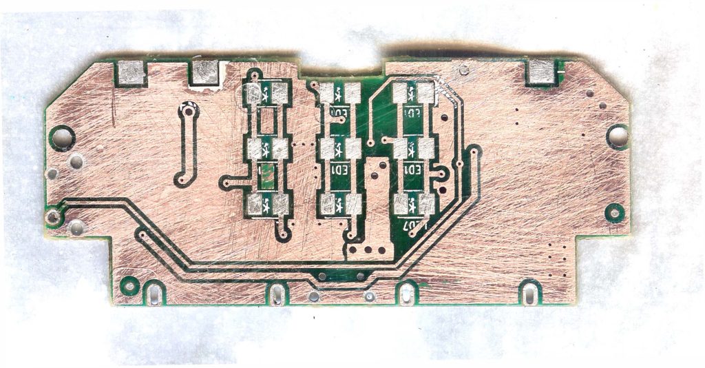
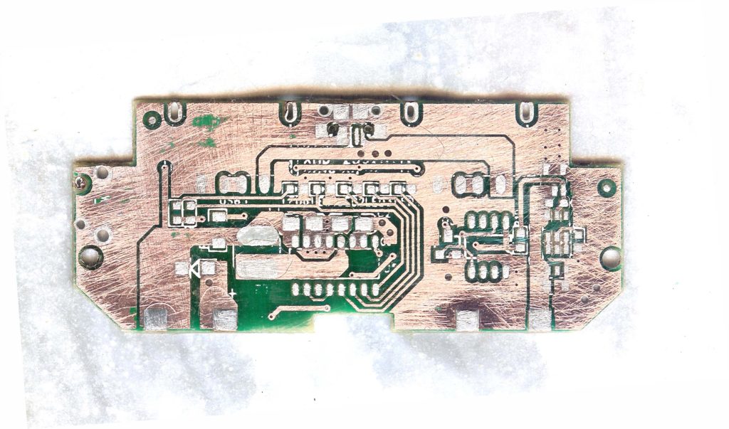
Reverse Engineering Wiring Diagram from existing PCB Board
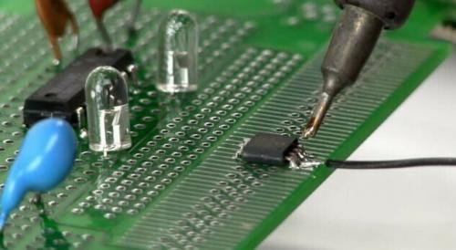
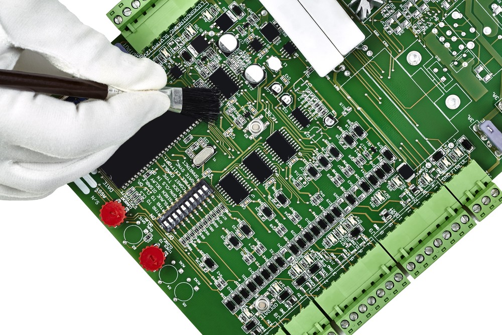
Reverse Engineering Wiring Diagram from existing PCB Board starts from desolder all the electronic parts off the circuit card, as well as stripping off the solder resist mask over the top and bottom layer;
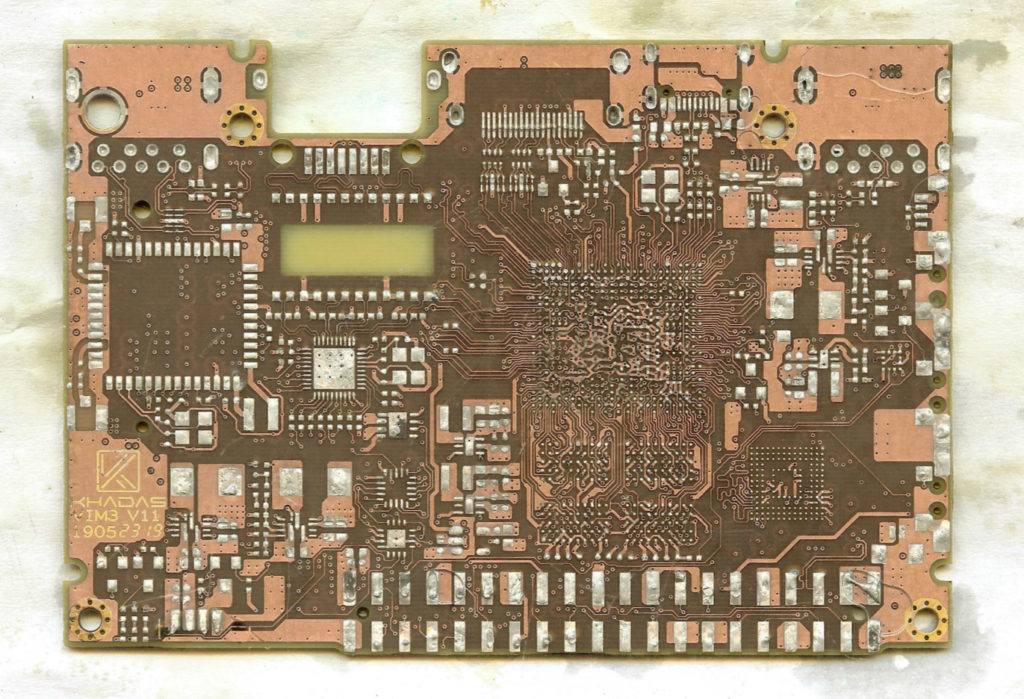
In the research of restoring schematic diagram from existing PCB Board, definition of Recreating existing PCB Board is regenerate PCB wiring diagram through PCB Board pattern file or directly draw it according to physical electronic PCB Board sample under the purpose of description of PCB Board principle and working environment.
Moreover, this wiring diagram from PCB Reverse engineering can also being used to analyze functional feature of electronic product.
Extract Wiring Diagram from Existing Circuit Board
Extract Wiring Diagram from Existing Circuit Board is able to help engineer to reproduce the printed circuit board which hasn’t been produced for a long time;
Checking and Optimization:
Whole process of extract wiring diagram from circuit board finish only after checking and testing done and approve pass, for nominal value of those distribution parameter sensitive components of circuit board need to check and optimizing, according to circuit board design, compare the extracted wiring diagram with circuit board design file to ensure the accuracy and completeness.