Archive for the ‘Break IC’ Category
 Restore IC Flash
 November 1st, 2012 |
  Author:
 Restore IC Flash memory content after disable the security fuse bit, crack Microcontroller protection and extract the code from MCU memory;
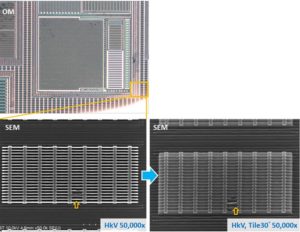
Restore IC Flash memory content after disable the security fuse bit, crack Microcontroller protection and extract the code from MCU memory
A non-invasive IC Flash Restore does not require any initial preparations of the device under test. The ic attacker can either tap the wires to the device, or plug it into a test circuit for the analysis. Once found, these ic breaks could be easily scaled and their reproduction does not involve very much cost. In addition, no tamper evidence is left after they are applied. Therefore they are considered to be the most serious threat to the hardware security of any device. At the same time it usually takes a lot of time and effort to find an ic copy on any particular device. This often involves reverse engineering the device in the sense of either disassembling its software or understanding its hardware layout.
 Posted in Break IC |
  Tags: chip flash restore, cpld flash restore, cypress ic flash restore, dsp flash restore, dsp mcu flash restore, fpga flash restore, mcu flash restore, pld flash restore, smartcard flash restore |
  Comments Closed
Break Chip ATmega1280 Flash
Break Chip ATmega1280 Flash memory normally is in the status of reading protective model, through our Microcontroller unlocking technique, flash memory and eeprom memory from ATmega1280 MCU can be readout;

Break Chip ATmega1280 Flash memory normally is in the status of reading protective model, through our Microcontroller unlocking technique, flash memory and eeprom memory from ATmega1280 MCU can be readout
Please view the chip ATMEGA1280 features for your reference:
The ATMEGA1280 has three lock bits that can be left unprogrammed (U) or can be programmed (P) to obtain the additional features listed in the following table.
When lock bit 1 is programmed, the logic level at the EA pin is sampled and latched during reset. If the device is powered up without a reset, the latch initializes to a random value and holds that value until reset is activated.
The latched value of EA must agree with the current logic level at that pin in order for the device to function properly. Once programmed, the lock bits can only be unprogrammed with the Chip Erase operations in either the parallel or serial modes before MCU PIC16F887 flash program attacking.
Atmel’s ATMEGA1280 Flash chip offers 12K bytes of in-system reprogrammable Flash Code memory. The ATMEGA1280 is normally shipped with the on-chip Flash Code memory array in the erased state (i.e. contents = FFH) and ready to be programmed.
This device supports a High-Voltage (12V) Parallel programming mode and a Low-Voltage (5V) Serial programming mode. The serial programming mode provides a convenient way to download the ATMEGA1280 inside the user’s system same as chip PIC18F66K90 flash attacking .
The parallel programming mode is compatible with conventional third party Flash or EPROM programmers. The Code memory array occupies one contiguous address space from 0000H to 2FFFH if break chip flash.
The Code array on the ATMEGA1280 is programmed byte-by-byte in either programming mode. An auto-erase cycle is provided with the self-timed programming operation in the serial programming mode before break chip flash.
There is no need to perform the Chip Erase operation to reprogram any memory location in the serial programming mode unless any of the lock bits have been programmed.
In the parallel programming mode, there is no auto-erase cycle. To reprogram any non-blank byte, the user needs to use the Chip Erase operation first to erase the entire Code memory array.
Decrypt IC Flash
Decrypt IC Flash memory, reset the Microcontroller security fuse bit when crack microcontroller using focus ion beam, and extract IC flash memory code in the format of heximal;
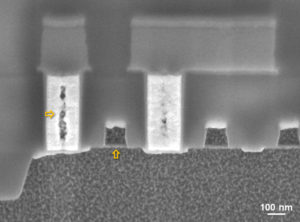
Decrypt IC Flash memory, reset the Microcontroller security fuse bit when crack microcontroller using focus ion beam, and extract IC flash memory code in the format of heximal
Invasive MCU breaking start with partial or full removal of the chip package in order to expose the silicon die. There are several methods, depending upon the package type and the requirements for further analysis. For microcontrollers, partial decapsulation is normally used, so that the device can be placed in a standard programmer unit and tested.
Some devices cannot be decapsulated and still maintain their electrical integrity. In this case the chip die has to be bonded to a chip carrier using a bonding machine which connects to the bonding pads on the die with thin aluminium or gold wire. Such bonding machines are available from different manufacturers and can be bought second-hand for less than £5,000. The contacts to the die can be also established using microprobing needles on a probing station.
To undertake further work under a FIB or a SEM the chip surface has to be coated with a thin gold layer making it conductive, otherwise it will very quickly accumulate charge and the picture become dark. We used an Emitech K550 gold sputter coater to coat samples prior to the FIB work. Some modern FIB machines have a built-in video camera for optical navigation, eliminating the need for the special coating.
Posted in Break IC |
Tags: cpld flash decrypt, cypress ic flash decrypt, dsp flash decrypt, dsp mcu flash decrypt, fpga flash decrypt, mcu flash decrypt, pld flash decrypt, smartcard flash decrypt |
Comments Closed
Break MCU ATmega1280V Eeprom
Break MCU ATmega1280V Eeprom memory for its data, and flash memory for its program, then extract files from both Microcontroller memories, disable the fuse bit by Microprocessor cracking;
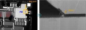
Break MCU ATmega1280V Eeprom memory for its data, and flash memory for its program, then extract files from both Microcontroller memories, disable the fuse bit by Microprocessor cracking
Please view the MCU ATMEGA1280V features for your reference:
To program and verify the AT89S53 in the parallel programming mode, the following sequence is recommended after break MCU eeprom:
Power-up sequence:
Apply power between VCC and GND pins.
Set RST pin to “H”.
Apply a 3 MHz to 24 MHz clock to XTAL1 pin and wait for at least 10 milliseconds to break MCU dsPIC30F4011 eeprom.
Set PSEN pin to “L”
ALE pin to “H”
EA pin to “H” and all other pins to “H”.
Apply the appropriate combination of “H” or “L” logic levels to pins P2.6, P2.7, P3.6, P3.7 to select one of the programming operations shown in the eeprom Programming Modes table.
Apply the desired byte address to pins P1.0 to P1.7 and P2.0 to P2.5.
Apply data to pins P0.0 to P0.7 for Write Code operation.
Raise EA/VPP to 12V to enable eeprom programming, erase or verification.
Pulse ALE/PROG once to program a byte in the Code memory array, or the lock bits. The byte-write cycle is self-timed and typically takes 1.5 ms.
To verify the byte just programmed, bring pin P2.7 to “L” and read the programmed data at pins P0.0 to P0.7.
Repeat steps 3 through 7 changing the address and data for the entire 12K-byte array or until the end of the object file is reached.
Power-off sequence will affect the process of break MCU SAF-C164CI-8EM firmware eeprom:
Set XTAL1 to “L”.
Set RST and EA pins to “L”.
Turn VCC power off.
The AT89S53 features DATA Polling to indicate the end of a write cycle. During a write cycle in the parallel or serial programming mode, an attempted read of the last byte written will result in the complement of the written datum on P0.7 (parallel mode), and on the MSB of the serial output byte on MISO (serial mode).
Once the write cycle has been completed, true data are valid on all outputs, and the next cycle may begin. DATA Polling may begin any time after a write cycle has been initiated.
The progress of byte programming in the parallel programming mode can also be monitored by the RDY/BSY output signal. Pin P3.4 is pulled Low after ALE goes High during programming to indicate BUSY. P3.4 is pulled High again when programming is done to indicate READY.
Reverse Engineering IC Flash
Reverse Engineering IC Flash is starting point of Microcontroller reverse engineering, target MCU will be delayer one by one in the reverse order of Microprocessor manufacturing, the purpose is to figure out the security fuse bit and cut it off;
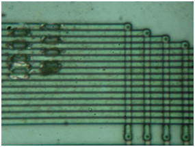
Reverse Engineering IC Flash is starting point of Microcontroller reverse engineering, target MCU will be delayer one by one in the reverse order of Microprocessor manufacturing, the purpose is to figure out the security fuse bit and cut it off
Read program and data out from Microcontroller memory requires direct access to the internal components of the device. If it is a security module or a USB dongle, then it has to be opened to get access to the internal memory chips. In the case of a smartcard or a microcontroller, the packaging should be removed followed by FIB or laser depassivation to get access to the internal wires buried deep under the passivation layer of the chip.
Such ic decryption method normally require a well equipped and knowledgeable ic attacker to succeed. Meanwhile, invasive ic extraction are becoming constantly more demanding and expensive, as feature sizes shrink and device complexity increases.
Posted in Break IC |
Tags: cpld flash reverse engineering, cypress ic flash reverse engineering, dsp flash reverse engineering, dsp mcu flash reverse engineering, fpga flash reverse engineering, mcu flash reverse engineering, pld flash reverse engineering, smartcard flash reverse engineering |
Comments Closed
Break IC Flash
Break IC flash could be also applied to the device communication protocol in order to find any hidden functions embedded by the software developer for testing and upgrade purposes.
Break IC flash could be also applied to the device communication protocol in order to find any hidden functions embedded by the software developer for testing and upgrade purposes
IC Chip manufacturers very often embed hardware test interfaces for postproduction testing of their semiconductor devices. If the security protection for these interfaces is not properly designed, the ic attacker can exploit it to get access to the on-chip memory. In smartcards such test interfaces are normally located outside the chip circuit and physically removed after the test operation, eliminating any possibility of use by outsiders.
Any security system, either software or hardware, could also have holes in its design and there is always a small chance that an ic cloner would eventually find one with brute force random testing. Careful design of the security protection, followed by proper evaluation, could help avoid many problems and make such MCU attack virtually impossible.
Posted in Break IC |
Tags: chip flash break, cpld flash break, cypress ic flash break, dsp flash break, dsp mcu flash break, fpga flash break, mcu flash break, pld flash break, smartcard flash break |
Comments Closed
Read IC Program
Another possible brute force ic decryption when you are trying to Read IC Program, applicable to many semiconductor chips, is applying an external high voltage signal (normally twice the power supply) to the chip’s pins to find out whether one of them has any transaction like entering into a factory test or programming mode.
Another possible brute force ic decryption when you are trying to Read IC Program, applicable to many semiconductor chips, is applying an external high voltage signal (normally twice the power supply) to the chip’s pins to find out whether one of them has any transaction like entering into a factory test or programming mode
In fact, such pins can be easily found with a digital multimeter because they do not have a protection diode to the power supply line. Once sensitivity to a high voltage is found for any pin, MCU Cracker can try a systematic search on possible combinations of logic signals applied to other pins to figure out which of them are used for the test/programming mode and exploit this opportunity.
Posted in Break IC |
Tags: cpld program read, cypress ic program read, dsp mcu program read, dsp program read, fpga program read, mcu program read, pld program read |
Comments Closed
Clone IC Program
Clone IC Program from memory which include flash and eeprom memory, reset the status of Microcontroller Chip from locked to open one;
Clone IC Program from memory which include flash and eeprom memory,
One of the most effective ways of IC Clone is by Brute force MCU cracking, can be also applied to a hardware design implemented into an ASIC or a CPLD. In this case the IC attacker tries to apply all possible logic combinations to the input of the device while observing all its outputs. That kind of ic break could be also called black-box analysis because the ic decryption expert does not have to know anything about the design of the device under test.
He only tries to understand the function of the device by trying all possible combinations of signals. This approach works well only for relatively small logic devices. Another problem when extracting program from IC memory will face is that designs implemented in CPLDs or ASICs have flip-flops, so the output will probably be function of both the previous state and the input. But the search space can be significantly reduced if the signals are observed and analysed beforehand. For example, clock inputs, data buses and some control signals could be easily identified, significantly reducing the area of search.
Posted in Break IC |
Tags: cpld program clone, cypress ic program clone, dsp mcu program clone, dsp program clone, fpga program clone, mcu program clone, pld program clone |
Comments Closed
Crack IC Flash
Crack IC Flash memory and extract the content inside flash memory, the program can be reprogramme to new MCU which can provide the same functions as originals;
Crack IC Flash memory and extract the content inside flash memory, the program can be reprogramme to new MCU which can provide the same functions as originals
‘Brute force’ has different meanings for cryptography and semiconductor hardware. A brute force MCU breaking would be defined as the methodical application of a large set of trials for a key to the system. This is usually done with a computer or an array of FPGAs delivering patterns at high speed and looking for success.
One example could be the password protection scheme used in microcontrollers, such as the Texas Instruments MSP430 family. The password itself is 32 bytes (256 bits) long which is more than enough to withstand direct brute force ic decode. But the password is allocated at the same memory addresses as the CPU interrupt vectors.
That, firstly, reduces the area of search as the vectors always point to even addresses within memory. Secondly, when the software gets updated, only a small part of the password is changed because most of the interrupt subroutines pointed to by the vectors are very likely to stay at the same addresses. As a result, if the ic breaker knows one of the previous passwords he could easily do a systematic search and find the correct password in a reasonable time.
Posted in Break IC |
Tags: chip flash crack, cpld flash crack, cypress ic flash crack, dsp flash crack, dsp mcu flash crack, fpga flash crack, mcu flash crack, pld flash crack, smartcard flash crack |
Comments Closed
Hack IC Program
Hack IC Program locked in the flash memory, remove the fuse bit of the Microcontroller by cracking technique, extract code from master MCU and reprogramme the file to new MCU;
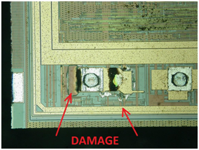
Hack IC Program locked in the flash memory, remove the fuse bit of the Microcontroller by cracking technique, extract code from master MCU and reprogramme the file to new MCU
As one of the most effective method of IC crack, To prevent these ic program attack happen, the designer should carefully calculate the number of CPU cycles that take place when the password is compared and make sure they are the same for correct and incorrect passwords. For example, in the Motorola 68HC08 microcontrollers family the internal ROM bootloader allows access to the Flash memory only if the correct eight-byte password was entered first. To achieve that, extra NOP commands were added to the program making the processing time equal for both correct and incorrect bytes of the password. That gives good protection against timing mcu attacks. Some microcontrollers have an internal RC generator mode of operation in which the CPU running frequency depends upon the power supply voltage and the die temperature. This makes timing analysis more difficult as the mcu cracker has to stabilize the device temperature and reduce any fluctuations and noise on the power supply line. Some smartcards have an internally randomised clock signal to make measurements of the time delays useless for the ic break.
Posted in Break IC |
Tags: cpld program hack, cypress ic program hack, dsp mcu program hack, dsp program hack, fpga program hack, mcu program hack, pld program hack |
Comments Closed