Archive for the ‘Break IC’ Category
 Microchip controller PIC18F25K80 Locked Memory Breaking
 June 19th, 2020 |
  Author:
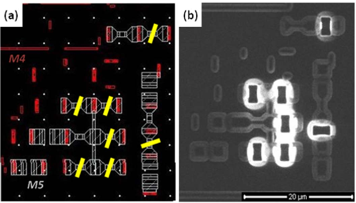
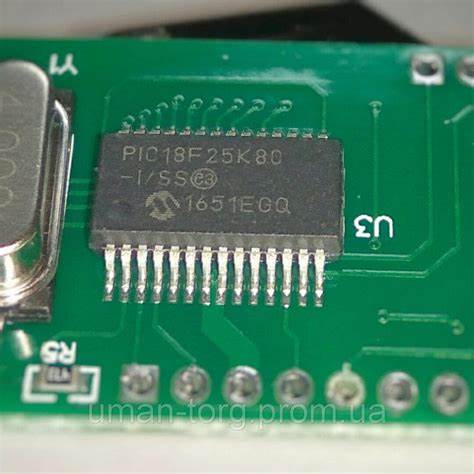
 Microchip controller PIC18F25K80 Locked Memory Breaking starts from unlock mcu pic18f25k80 fuse bit by focus ion beam and readout microprocessor flash heximal;
All of the devices in the PIC18F25K80 family incorpo- rate a range of features that can significantly reduce power consumption during operation. Key items include:
La mémoire du programme flash du microcontrôleur sécurisé par puce PIC18F25K80 et la décapsulation de la mémoire de données eeprom commencent à partir du décryptage du MCU de protection PIC18F25K80 fusible par faisceau d’ions focalisé et extrait le microprocesseur crypté PIC18F25K80 du micrologiciel intégré du fichier binaire ou des données heximales ;
- Alternate Run Modes: By clocking the controller from the Timer1 source or the Internal RC oscilla- tor, power consumption during code execution can be reduced.
- Multiple Idle Modes: The controller can also run with its CPU core disabled but the peripherals still active. In these states, power consumption can be reduced even further.
- On-the-Fly Mode Switching: The power-managed modes are invoked by user code during operation, allowing the user to incorporate power-saving ideas into their application’s software design.
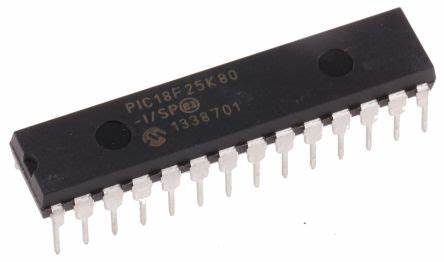
마이크로칩 보안 마이크로컨트롤러 PIC18F25K80 플래시 프로그램 메모리 및 eeprom 데이터 메모리 캡슐화는 포커스 이온 빔에 의한 보호 MCU PIC18F25K80 퓨즈 비트를 해독하고 바이너리 파일 또는 16진수 데이터의 암호화된 마이크로프로세서 PIC18F25K80 내장 펌웨어를 추출하는 것부터 시작됩니다.
XLP: An extra low-power BOR and low-power Watchdog timer
All of the devices in the PIC18F25K80 family offer different oscillator options, allowing users a range of choices in developing application hardware as well as unlocking pic18f26k80 flash memory. These include:
- External Resistor/Capacitor (RC); RA6 available
- External Resistor/Capacitor with Clock Out (RCIO)
- Three External Clock modes:
- External Clock (EC); RA6 available
- External Clock with Clock Out (ECIO)
External Crystal (XT, HS, LP)
- A Phase Lock Loop (PLL) frequency multiplier, available to the external oscillator modes which allows clock speeds of up to 64 MHz. PLL can also be used with the internal oscillator.
- An internal oscillator block that provides a 16 MHz clock (±2% accuracy) and an INTOSC source (approximately 31 kHz, stable over temperature and VDD)
- Operates as HF-INTOSC or MF-INTOSC when block is selected for 16 MHz or 500 kHz
- Frees the two oscillator pins for use as additional general purpose I/O
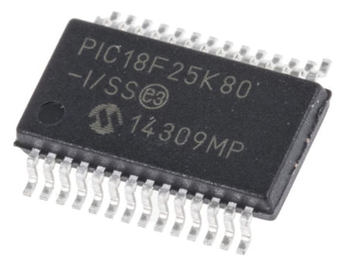
माइक्रोचिप सुरक्षित माइक्रोकंट्रोलर PIC18F25K80 फ्लैश प्रोग्राम मेमोरी और ईप्रोम डेटा मेमोरी डिकैप्सुलेशन फोकस आयन बीम द्वारा डिक्रिप्ट सुरक्षात्मक MCU PIC18F25K80 फ्यूज बिट से शुरू होता है और एन्क्रिप्टेड माइक्रोप्रोसेसर PIC18F25K80 बाइनरी फ़ाइल या हेक्सिमल डेटा के एम्बेडेड फर्मवेयर को निकालता है;
The internal oscillator block provides a stable reference source that gives the family additional features for robust operation:
 Posted in
Microprocessor PIC18F46K20 Flash Program Replication
Microprocessor PIC18F46K20 Flash Program Replication needs to crack mcu pic18f46k20 fuse bit by focus ion beam and extract code from embedded IC chip memory;
The Table Pointer (TBLPTR) register addresses a byte within the program memory. The TBLPTR is comprised of three SFR registers: Table Pointer Upper Byte, Table Pointer High Byte and Table Pointer Low Byte (TBLPTRU:TBLPTRH:TBLPTRL).
These three registers join to form a 22-bit wide pointer. The low-order 21 bits allow the device to address up to 2 Mbytes of program memory space. The 22nd bit allows access to the device ID, the user ID and the Configuration bits will be required also in the process of pic18f24k20 program and data recovery.
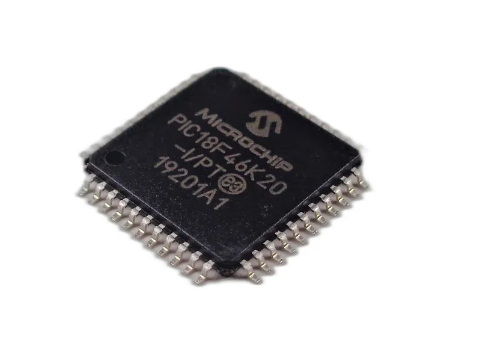
La replica del programma flash del microprocessore protetto PIC18F46K20 necessita di crackare il fusibile protetto dell’MCU PIC18F46K20 tramite raggio ionico focalizzato ed estrarre il codice sorgente dal controller del microchip incorporato Dati binari della memoria flash PIC18F46K20 e file esagonale della memoria eeprom;
The Table Pointer register, TBLPTR, is used by the TBLRD and TBLWT instructions. These instructions can update the TBLPTR in one of four ways based on the table operation. These operations are shown in Table 6-2. These operations on the TBLPTR affect only the low-order 21 bits.
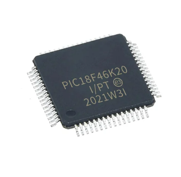
wyodrębnij kod źródłowy zabezpieczonego mikrokontrolera PIC18F26J13 zaczynając od bitu bezpiecznika zabezpieczającego PIC18F26J13 mikroprocesora i zrzuć wbudowane oprogramowanie sprzętowe w formacie pliku binarnego lub danych szesnastkowych z zablokowanej pamięci flash MCU PIC18F26J13 lub pamięci eeprom;
TBLPTR is used in reads, writes and erases of the Flash program memory. When a TBLRD is executed, all 22 bits of the TBLPTR determine which byte is read from program memory directly into the TABLAT register. When a TBLWT is executed the byte in the TABLAT register is written, not to Flash memory but, to a holding register in preparation for a program memory write.
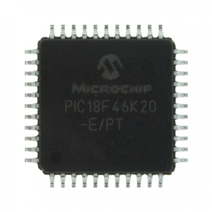
يبدأ استخراج الكود المصدري لوحدة التحكم الدقيقة المؤمنة PIC18F26J13 من وحدة حماية المعالج الدقيق PIC18F26J13 وتفريغ البرامج الثابتة المضمنة بتنسيق ملف ثنائي أو بيانات سداسية من ذاكرة فلاش MCU المقفلة PIC18F26J13 أو ذاكرة eeprom؛
The holding registers constitute a write block which varies depending on the device.The 3, 4, or 5 LSbs of the TBLPTRL register determine which specific address within the holding register block is written to. The MSBs of the Table Pointer have no effect during TBLWT operations.
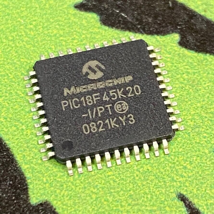
Attack Microchip PIC18F45K20 MCU Memory Protection
Attack Microchip PIC18F45K20 MCU Memory Protection and unlock microcontroller pic18f45k20 flash and eeprom memory, read embedded heximal from mcu with programmer;
The table read operation retrieves one byte of data directly from program memory and places it into the TABLAT register.
The table write operation stores one byte of data from the TABLAT register into a write block holding register. The procedure to write the contents of the holding registers into program memory is detailed in Section 6.5 “Writing to Flash Program Memory”.
Figure 6-2 shows the operation of a table write with program memory and data RAM. Table operations work with byte entities. Tables contain- ing data, rather than program instructions, are not required to be word aligned. Therefore, a table can start and end at any byte address. If a table write is being used to write executable code into program memory, program instructions will need to be word aligned for pic18f43k20 flash memory breaking.

protezione della memoria MCU del microchip PIC18F45K20 protetta dall’attacco e sblocco protetto della memoria flash ed eeprom del microcontrollore PIC18F45K20, lettura dei dati esagonali incorporati o del codice sorgente binario dalla memoria flash crittografata PIC18F45K20 del microprocessore e dal firmware incorporato della memoria eeprom con programmatore;
The EECON1 register (Register 6-1) is the control register for memory accesses. The EECON2 register is not a physical register; it is used exclusively in the memory write and erase sequences. Reading EECON2 will read all ‘0’s.
The EEPGD control bit determines if the access will be a program or data EEPROM memory access. When EEPGD is clear, any subsequent operations will operate on the data EEPROM memory.

zabezpieczony przed atakiem mikrochip PIC18F45K20 ochrona pamięci MCU i odblokowanie chronionego mikrokontrolera PIC18F45K20 pamięć flash i eeprom, odczyt osadzonych danych szesnastkowych lub binarnego kodu źródłowego z zaszyfrowanej mikroprocesorem pamięci flash PIC18F45K20 i wbudowanego oprogramowania sprzętowego pamięci eeprom z programatorem;
When EEPGD is set, any subsequent operations will operate on the program memory. The CFGS control bit determines if the access will be to the Configuration/Calibration registers or to program memory/data EEPROM memory.
When CFGS is set, subsequent operations will operate on Configuration registers regardless of EEPGD (see Section 23.0“Special Features of the CPU”). When CFGS is clear, memory selection access is determined by EEPGD.
مهاجمة حماية ذاكرة الرقاقة الدقيقة PIC18F45K20 MCU وفتح وحدة التحكم الدقيقة المحمية PIC18F45K20 ذاكرة فلاش وذاكرة eeprom، وقراءة البيانات السداسية المضمنة أو كود المصدر الثنائي من ذاكرة فلاش PIC18F45K20 المشفرة بالمعالج الدقيق والبرامج الثابتة المضمنة بذاكرة eeprom مع مبرمج؛
Break PIC18F43K20 Microcontroller Flash Memory
Break PIC18F43K20 Microcontroller Flash Memory is a process to crack mcu pic18f43k20 fuse bit by focus ion beam and then readout MCU heximal;
Enabling the PIC18 extended instruction set (XINST Configuration bit = 1) significantly changes certain aspects of data memory and its addressing. Specifi- cally, the use of the Access Bank for many of the core PIC18 instructions is different; this is due to the intro- duction of a new addressing mode for the data memory space.
quebrar a memória flash do microcontrolador de proteção PIC18F43K20 é um processo para desabilitar / atacar o bit de fusível MCU PIC18F43K20 protegido por feixe de íons de foco e, em seguida, ler o firmware incorporado do microprocessador criptografado por microchip, memória flash PIC18F43K20 e memória eeprom no formato de código-fonte heximal ou dados de arquivo binário;
What does not change is just as important. The size of the data memory space is unchanged, as well as its linear addressing. The SFR map remains the same. Core PIC18 instructions can still operate in both Direct and Indirect Addressing mode; inherent and literal instructions do not change at all. Indirect addressing with FSR0 and FSR1 also remain unchanged.

взлом флэш-памяти защитного микроконтроллера PIC18F43K20 – это процесс отключения / атаки защищенного плавкого бита MCU PIC18F43K20 с помощью фокуса ионного луча, а затем считывания встроенной прошивки из зашифрованной микрочипом флэш-памяти микропроцессора PIC18F43K20 и памяти EEPROM в формате шестнадцатеричного исходного кода или данных двоичного файла;
Enabling the PIC18 extended instruction set changes the behavior of indirect addressing using the FSR2 register pair within Access RAM. Under the proper conditions, instructions that use the Access Bank – that is, most bit-oriented and byte-oriented instructions – can invoke a form of indexed addressing using an offset specified in the instruction by . This special addressing mode is known as Indexed Addressing with Literal Offset, or Indexed Literal Offset mode by breaking mcu pic18f14k22 flash memory;
شکستن حافظه فلش میکروکنترلر محافظ PIC18F43K20 فرآیندی است برای غیرفعال کردن/حمله کردن فیوز ایمن MCU PIC18F43K20 توسط پرتو یونی فوکوس و سپس بازخوانی سیستم عامل تعبیه شده از ریزپردازنده رمزگذاری شده با ریزتراشه PIC18F43K20 حافظه فلش منبع و حافظه فایل کد باینری eeprom با فرمت یا فرمت Head.
When using the extended instruction set, this addressing mode requires the following:
- The use of the Access Bank is forced (‘a’ = 0) and
The file address argument is less than or equal to 5Fh.
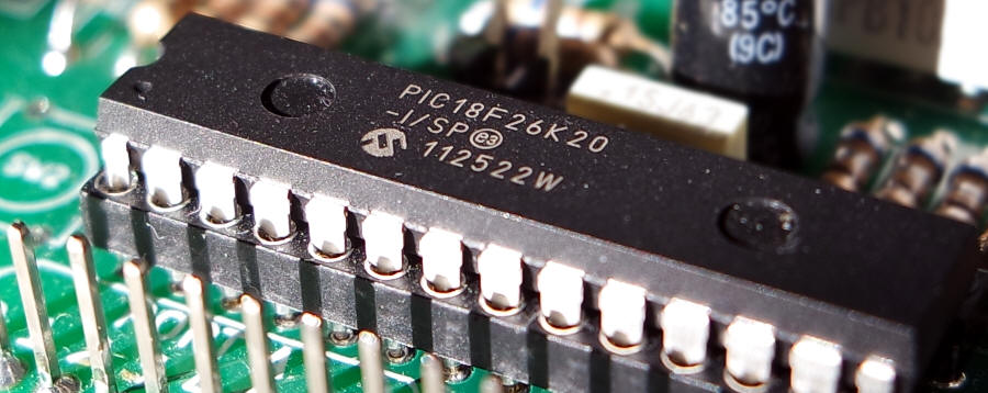
Duplicate Microchip MCU PIC18F26K20 Source Code
Duplicate Microchip MCU PIC18F26K20 Source Code needs to crack microcontroller pic18f26k20 flash and eeprom memory, read the embedded firmware out from microcontroller;
The Access RAM bit ‘a’ determines how the address is interpreted. When ‘a’ is ‘1’, the contents of the BSR (Section 5.3.1 “Bank Select Register (BSR)”) are used with the address to determine the complete 12-bit address of the register. When ‘a’ is ‘0’, the address is interpreted as being a register in the Access Bank. Addressing that uses the Access RAM is sometimes also known as Direct Forced Addressing mode.
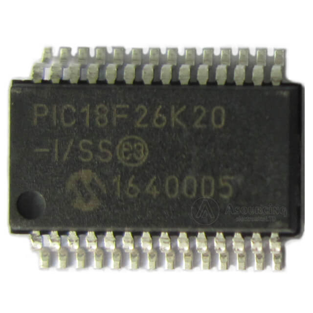
o código-fonte criptografado MCU PIC18F26K20 protegido por Microchip duplicado precisa quebrar a memória flash e eeprom do microcontrolador protetor PIC18F26K20, despejar o firmware incorporado do microprocessador PIC18F26K20 com bits bloqueados como um software binário ou arquivo de dados heximal;
A few instructions, such as MOVFF, include the entire 12-bit address (either source or destination) in their opcodes. In these cases, the BSR is ignored entirely. The destination of the operation’s results is determined by the destination bit ‘d’. When ‘d’ is ‘1’, the results are stored back in the source register, overwriting its origi- nal contents.
When ‘d’ is ‘0’, the results are stored in the W register. Instructions without the ‘d’ argument have a destination that is implicit in the instruction; their destination is either the target register being operated on or the W register.
дубликат зашифрованного исходного кода MCU PIC18F26K20, защищенного микрочипом, необходимо взломать защитную флэш-память микроконтроллера PIC18F26K20 и память EEPROM, выгрузить встроенную прошивку из микропроцессора PIC18F26K20 с заблокированными битами в виде двоичного программного обеспечения или шестнадцатеричного файла данных;
Indirect addressing allows the user to access a location in data memory without giving a fixed address in the instruction. This is done by using File Select Registers (FSRs) as pointers to the locations which are to be read or written. Since the FSRs are themselves located in RAM as Special File Registers, they can also be directly manipulated under program control.
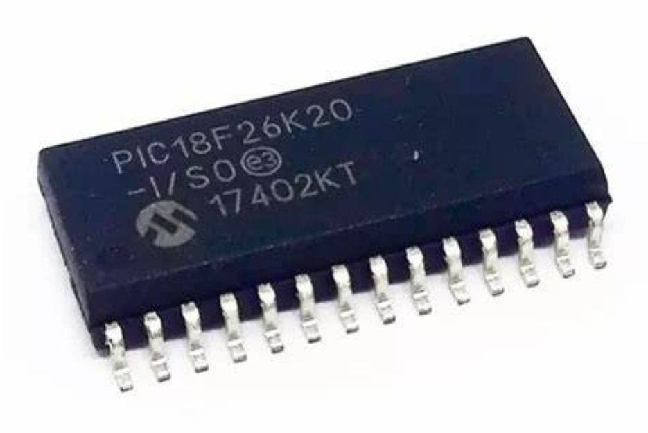
کد منبع رمزگذاری شده MCU PIC18F26K20 ایمن شده با ریزتراشه تکراری نیاز به شکستن میکروکنترلر محافظ PIC18F26K20 فلش و حافظه eeprom دارد، سیستم عامل تعبیه شده را از ریزپردازنده PIC18F26K20 با بیت های قفل شده به عنوان یک نرم افزار باینری یا فایل داده هگزیمال خارج می کند.
This makes FSRs very useful in implementing data structures, such as tables and arrays in data memory. The registers for indirect addressing are also implemented with Indirect File Operands (INDFs) that permit automatic manipulation of the pointer value with auto-incrementing, auto-decrementing or offsetting with another value to increase the success rate of pic18f13k22 microchip microcontroller attacking. This allows for efficient code, using loops, such as the example of clearing an entire RAM bank
Revese Microcontroller PIC18F25K20 Locked Heximal
Revese Microcontroller PIC18F25K20 Locked Heximal is a way to crack mcu pic18f25k20 fuse bit and extract embedded code from flash memory;
While the program memory can be addressed in only one way – through the program counter – information in the data memory space can be addressed in several ways. For most instructions, the addressing mode is fixed. Other instructions may use up to three modes, depending on which operands are used and whether or not the extended instruction set is enabled.
The addressing modes are:
- Inherent
- Literal
- Direct
- Indirect
- Literal
An additional addressing mode, Indexed Literal Offset, is available when the extended instruction set is enabled (XINST Configuration bit = 1). Its operation is discussed in greater detail in Section 5.5.1 “Indexed Addressing with Literal Offset”.
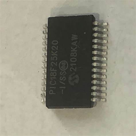
Защищенный микроконтроллер Revese Engineering PIC18F25K20 заблокированным шестнадцатеричным файлом или двоичными данными – это способ взлома защитного микроконтроллера PIC18F25K20 бита предохранителя и извлечения исходного кода встроенной прошивки из зашифрованного микропроцессора PIC18F25K20 флэш-памяти и памяти EEPROM;
Many PIC18 control instructions do not need any argu- ment at all; they either perform an operation that glob- ally affects the device or they operate implicitly on one register. This addressing mode is known as Inherent Addressing.
Examples include SLEEP, RESET and DAW. Other instructions work in a similar way but require an additional explicit argument in the opcode when breaking microchip mcu pic18f14k50 flash memory. This is known as Literal Addressing mode because they require some literal value as an argument. Examples include ADDLW and MOVLW, which respectively, add or move a literal value to the W register. Other examples include CALL and GOTO, which include a 20-bit program memory address.
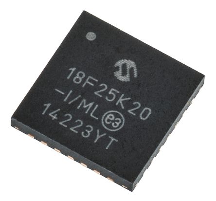
revese engenharia microcontrolador seguro PIC18F25K20 bloqueado arquivo heximal ou dados binários é uma maneira de quebrar MCU protetor PIC18F25K20 fusível bit e extrair o código-fonte de firmware incorporado do microprocessador criptografado PIC18F25K20 memória flash e memória eeprom;
Direct addressing specifies all or part of the source and/or destination address of the operation within the opcode itself. The options are specified by the arguments accompanying the instruction. In the core PIC18 instruction set, bit-oriented and byte-oriented instructions use some version of direct addressing by default which can faciliate the process of pic18f23k20 memory unit attacking.
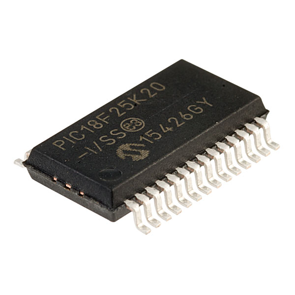
revese مهندسی میکروکنترلر امن PIC18F25K20 فایل هگزیمال قفل شده و یا داده های باینری یک راه برای کرک محافظ MCU PIC18F25K20 فیوز بیت و استخراج کد منبع سیستم عامل تعبیه شده از ریزپردازنده رمزگذاری شده PIC18F25K20 حافظه فلش و حافظه eeprom است؛
All of these instructions include some 8-bit literal address as their Least Significant Byte. This address specifies either a register address in one of the banks of data RAM (Section 5.3.3 “GeneralPurpose Register File”) or a location in the Access Bank (Section 5.3.2 “Access Bank”) as the data source for the instruction.
Recovery Protected Microcontroller PIC18F24K20 Program and Data
Recovery Protected Microcontroller PIC18F24K20 Program and Data from locked flash and eeprom memory needs to crack pic18f24k20 mcu protective system and disable the tamper resistance, then extract code from IC chip pic18f24k20;

- Memory Endurance: The Flash cells for both program memory and data EEPROM are rated to last for many thousands of erase/write cycles – up to 10K for program memory and 100K for EEPROM. Data retention without refresh is conservatively estimated to be greater than 40 years.
- Self-programmability: These devices can write to their own program memory spaces under inter- nal software control. By using a bootloader rou- tine located in the protected Boot Block at the top of program memory, it becomes possible to create an application that can update itself in the field.

Защищенный микроконтроллер для восстановления PIC18F24K20 встроенной прошивки Данные флэш-памяти и EEPROM из заблокированной флэш-памяти и памяти EEPROM должны взломать защищенный микропроцессор PIC18F24K20 систему защиты от несанкционированного доступа и отключить защиту, затем считывать исходный код в формате двоичного файла или шестнадцатеричных данных с зашифрованных микросхемами PIC18F24K20;
- Extended Instruction Set: The PIC18F2XK20/ 4XK20 family introduces an optional extension to the PIC18 instruction set, which adds 8 new instructions and an Indexed Addressing mode. This extension, enabled as a device configuration option, has been specifically designed to optimize re-entrant application code originally developed in high-level languages, such as C.
- Enhanced CCP module: In PWM mode, this module provides 1, 2 or 4 modulated outputs for controlling half-bridge and full-bridge drivers. Other features include:
- Auto-Shutdown, for disabling PWM outputs on interrupt or other select conditions
- Auto-Restart, to reactivate outputs once the condition has cleared
- Output steering to selectively enable one or more of 4 outputs to provide the PWM signal.
- Enhanced Addressable USART: This serial communication module is capable of standard
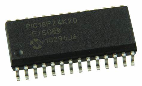
recuperação protegida microcontrolador PIC18F24K20 incorporado firmware flash programa e dados eeprom de flash bloqueado e memória eeprom precisa quebrar microprocessador seguro PIC18F24K20 sistema de resistência a violação e desativar a segurança, em seguida, ler o código-fonte no formato de arquivo binário ou dados heximal de microchip criptografado MCU PIC18F24K20;
RS-232 operation and provides support for the LIN bus protocol. Other enhancements include automatic baud rate detection and a 16-bit Baud Rate Generator for improved resolution. When the microcontroller is using the internal oscillator block, the USART provides stable operation for applications that talk to the outside world without using an external crystal (or its accompanying power requirement).
- 10-bit A/D Converter: This module incorporates programmable acquisition time, allowing for a channel to be selected and a conversion to be initiated without waiting for a sampling period and thus, reduce code overhead which can effectively increase the success rate of mcu pic18f4450 memory data recovery.
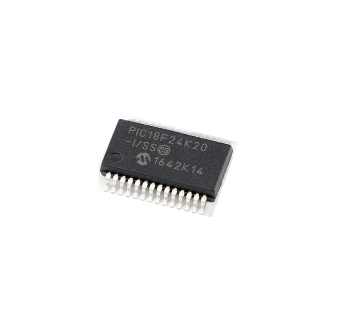
بازیابی میکروکنترلر محافظت شده PIC18F24K20 برنامه فلش سیستم عامل تعبیه شده و داده های eeprom از فلش قفل شده و حافظه eeprom نیاز به شکستن ریزپردازنده امن PIC18F24K20 سیستم مقاومت در برابر دستکاری و غیر فعال کردن امنیت، سپس کد منبع را در قالب فایل باینری یا داده های هگزیمال از میکروچیپ رمزگذاری شده MCU PIC18F24K20 بخوانید؛
Extended Watchdog Timer (WDT): This enhanced version incorporates a 16-bit postscaler, allowing an extended time-out range that is stable across operating voltage and temperature. See Section 26.0 “Electrical Characteristics” for time-out periods.
Attack Microchip MCU PIC18F23K20 Memory Unit
Attack Microchip MCU PIC18F23K20 Memory Unit and extract locked heximal from embedded microcontroller after crack microprocessor pic18f23k20 security fuse bit;
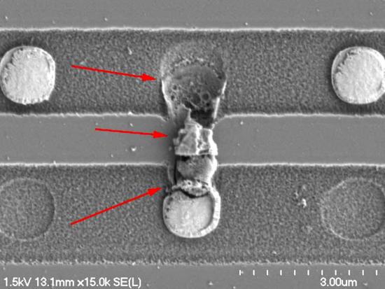
All of the devices in the PIC18F23K20 family incorporate a range of features that can significantly reduce power consumption during operation. Key items include:
- Alternate Run Modes: By clocking the controller from the Timer1 source or the internal oscillator block, power consumption during code execution can be reduced by as much as 90%.
- Multiple Idle Modes: The controller can also run with its CPU core disabled but the peripherals still active. In these states, power consumption can be reduced even further, to as little as 4% of normal operation requirements.
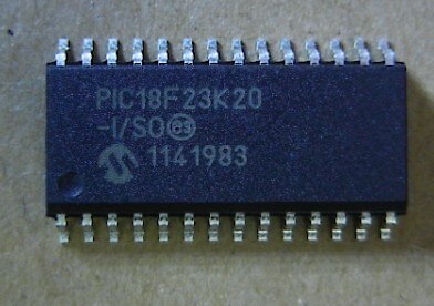
atacar o bit de fusível de segurança MCU PIC18F23K20 protegido pela Microchip e extrair dados heximais bloqueados ou arquivo binário da memória de programa flash do microcontrolador PIC18F23K20 incorporado ou memória de dados eeprom;
- On-the-fly Mode Switching: The power- managed modes are invoked by user code during operation, allowing the user to incorporate power- saving ideas into their application’s software design.
- Low Consumption in Key Modules: The power requirements for both Timer1 and the Watchdog Timer are minimized. See Section 26.0 “Electrical Characteristics” for values.
All of the devices in the PIC18F2XK20/4XK20 family offer ten different oscillator options, allowing users a wide range of choices in developing application hardware. These include:
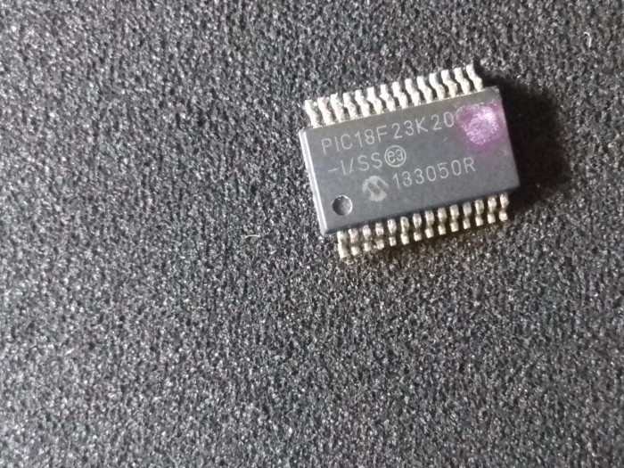
حمله میکروچیپ ایمن MCU PIC18F23K20 بیت فیوز امنیتی و استخراج داده های هگزیمال قفل شده یا فایل باینری از حافظه برنامه فلش میکروکنترلر تعبیه شده PIC18F23K20 یا حافظه داده eeprom.
- Four Crystal modes, using crystals or ceramic resonators
- Two External Clock modes, offering the option of using two pins (oscillator input and a divide-by-4 clock output) or one pin (oscillator input, with the second pin reassigned as general I/O)
- Two External RC Oscillator modes with the same pin options as the External Clock modes
- An internal oscillator block which contains a 16 MHz HFINTOSC oscillator and a 31 kHz LFINTOSC oscillator which together provide 8
user selectable clock frequencies, from 31 kHz to 16 MHz. This option frees the two oscillator pins for use as additional general purpose I/O. A Phase Lock Loop (PLL) frequency multiplier, available to both the high-speed crystal and internal oscillator modes which can be manipulted for breaking microcontroller pic18f14k50 memory, which allows clock speeds of up to 64 MHz.
атаковать микрочип, защищенный битом предохранителя MCU PIC18F23K20, и извлечь заблокированные шестнадцатеричные данные или двоичный файл из встроенной флэш-памяти программ микроконтроллера PIC18F23K20 или памяти данных EEPROM;
Used with the internal oscillator, the PLL gives users a complete selection of clock speeds, from 31 kHz to 64 MHz – all without using an external crystal or clock circuit.
Microcontroller PIC18F13K50 Flash Memory Attacking
Microcontroller PIC18F13K50 Flash Memory Attacking needs to crack pic18f13k50 protective system and read embedded heximal from mcu pic18f13k50;
- Memory Endurance: The Flash cells for both program memory and data EEPROM are rated to last for many thousands of erase/write cycles – up to 1K for program memory and 100K for EEPROM. Data retention without refresh is conservatively estimated to be greater than 40 years which has provide the PIC18F2520 flash binary recovery become possible.
- Self-programmability: These devices can write to their own program memory spaces under internal software control. Using a bootloader routine located in the code protected Boot Block, it is possible to create an application that can update itself in the field.
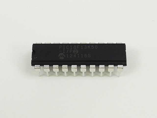
memória flash do microcontrolador seguro PIC18F13K50 e ataque à memória eeprom precisa quebrar o sistema de proteção do microprocessador PIC18F13K50 e ler o firmware incorporado no formato de dados heximais ou arquivo binário do MCU PIC18F13K50 criptografado;
- Extended Instruction Set: The PIC18(L)F1XK50 family introduces an optional extension to the PIC18 instruction set, which adds eight new instructions and an Indexed Addressing mode. This extension has been specifically designed to optimize re-entrant application code originally developed in high-level languages, such as C.
- Enhanced CCP module: In PWM mode, this module provides 1, 2 or 4 modulated outputs for controlling half-bridge and full-bridge drivers. Other features include:
- Auto-Shutdown, for disabling PWM outputs on interrupt or other select conditions
- Auto-Restart, to reactivate outputs once the condition has cleared
- Output steering to selectively enable one or more of four outputs to provide the PWM signal.
- Enhanced Addressable USART: This serial communication module is capable of standard
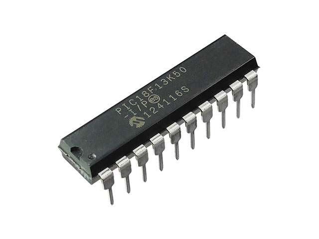
میکروکنترلر ایمن فلش مموری PIC18F13K50 و حمله به حافظه eeprom باید سیستم حفاظتی ریزپردازنده PIC18F13K50 را شکسته و سیستم عامل تعبیه شده را در قالب داده هگزیمال یا فایل باینری از MCU رمزگذاری شده PIC18F13K50 بخواند.
RS-232 operation and provides support for the LIN bus protocol. Other enhancements include automatic baud rate detection and a 16-bit Baud Rate Generator for improved resolution.
- 10-bit A/D Converter: This module incorporates programmable acquisition time, allowing for a channel to be selected and a conversion to be initiated without waiting for a sampling period and thus, reduce code overhead.
Extended Watchdog Timer (WDT): This enhanced version incorporates a 16-bit postscaler, allowing an extended time-out range that is stable across operating voltage and temperature.
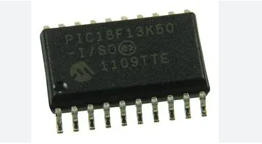
атака защищенной флэш-памяти микроконтроллера PIC18F13K50 и памяти EEPROM требует взлома защитной системы микропроцессора PIC18F13K50 и считывания встроенной прошивки в формате шестнадцатеричных данных или двоичного файла из зашифрованного MCU PIC18F13K50;
Microchip Processor PIC18F14K50 Flash Memory Breaking
Microchip Processor PIC18F14K50 Flash Memory Breaking is a process to crack pic18f14k50 microcontroller fuse bit and then extract heximal from IC chip memory.
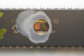
All of the devices in the PIC18(L)F1XK50 family incor- porate a range of features that can significantly reduce power consumption during operation. Key items include:
- Alternate Run Modes: By clocking the controller from the Timer1 source or the internal oscillator block, power consumption during code execution can be reduced by as much as 90%.
- Multiple Idle Modes: The controller can also run with its CPU core disabled but the peripherals still active. In these states, power consumption can be reduced even further, to as little as 4% of normal operation requirements.
- On-the-fly Mode Switching: The power- managed modes are invoked by user code during operation, allowing the user to incorporate power- saving ideas into their application’s software design.
- Low Consumption in Key Modules: The power requirements for both Timer1 and the Watchdog Timer are minimized. See Section 27.0 “Electrical Specifications” for values.
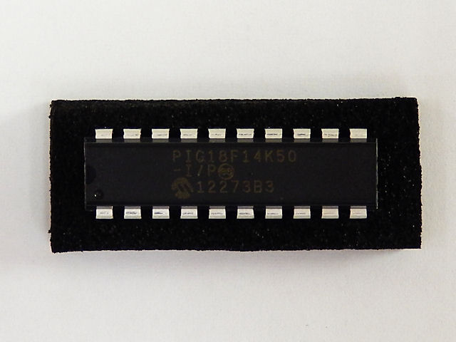
crackear la protección de la memoria del MCU del microchip PIC18F14K50 protegido y recuperar el contenido flash del microcontrolador PIC18F14K50 protegido y el software eeprom de la memoria, copiar datos heximales incorporados o código fuente binario del microprocesador PIC18F14K50 cifrado;
All of the devices in the PIC18(L)F1XK50 family offer ten different oscillator options, allowing users a wide range of choices in developing application hardware. These include:
- Four Crystal modes, using crystals or ceramic resonators
- External Clock modes, offering the option of using two pins (oscillator input and a divide-by-4 clock output) or one pin (oscillator input, with the second pin reassigned as general I/O)
- External RC Oscillator modes with the same pin options as the External Clock modes
- An internal oscillator block which contains a 16 MHz HFINTOSC oscillator and a 31 kHz LFINTOSC oscillator which together provide 8
- user selectable clock frequencies, from 31 kHz to 16 MHz. This option frees the two oscillator pins for use as additional general purpose I/O.
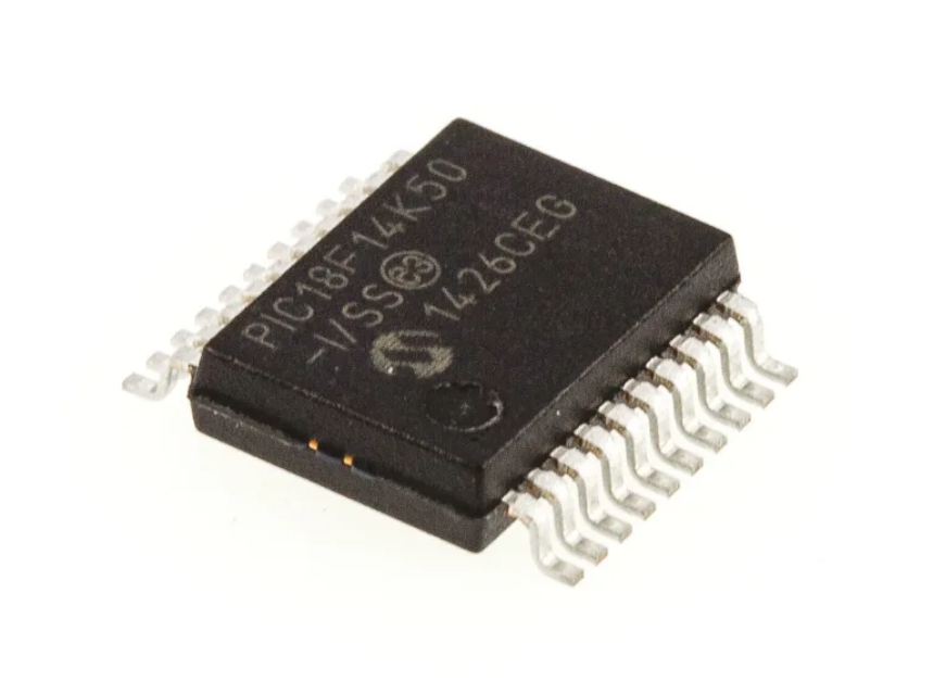
كسر حماية ذاكرة الشريحة الدقيقة PIC18F14K50 MCU واستعادة محتوى الفلاش المحمي PIC18F14K50 وبرنامج eeprom من الذاكرة، ونسخ البيانات السداسية المضمنة أو كود المصدر الثنائي من المعالج الدقيق المشفر PIC18F14K50؛
- A Phase Lock Loop (PLL) frequency multiplier, available to both the high-speed crystal and inter- nal oscillator modes, which allows clock speeds of up to 48 MHz. Used with the internal oscillator, the PLL gives users a complete selection of clock speeds, from 31 kHz to 32 MHz – all without using an external crystal or clock circuit which is a critical flaw for cracking pic18f4550 mcu memory.
Besides its availability as a clock source, the internal oscillator block provides a stable reference source that gives the family additional features for robust operation:
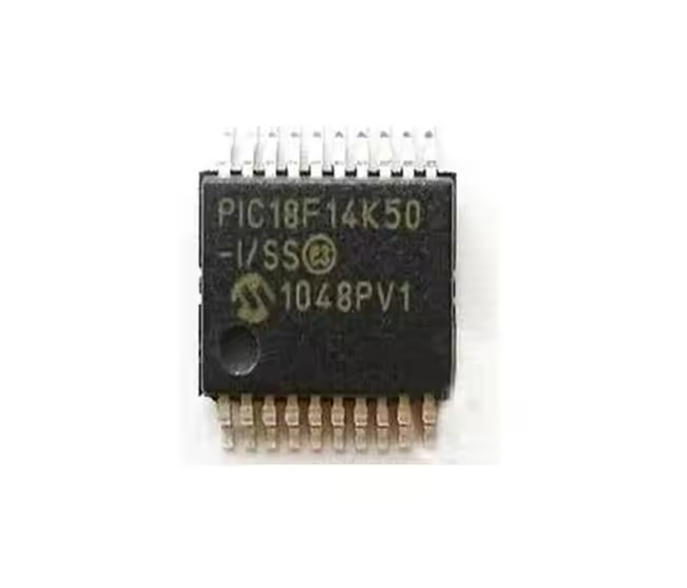
सुरक्षित माइक्रोचिप PIC18F14K50 MCU मेमोरी सुरक्षा को क्रैक करें और मेमोरी से संरक्षित माइक्रोकंट्रोलर PIC18F14K50 फ़्लैश सामग्री और ईप्रोम सॉफ़्टवेयर को पुनर्प्राप्त करें, माइक्रोप्रोसेसर एन्क्रिप्टेड PIC18F14K50 से एम्बेडेड हेक्सिमल डेटा या बाइनरी स्रोत कोड की प्रतिलिपि बनाएँ;