Archive for the ‘Break IC’ Category
 STMicrocontroller STM8L052C6T6 Locked Flash Memory Decryption
 January 1st, 2021 |
  Author:
 The stm8l052c6t6 is a compact low-power mcu from stmicro designed for embedded products where energy efficiency, reliable control, and long operating life are important. Its capabilities make this microcontroller suitable for applications including industrial monitoring, smart meters, battery-powered instruments, consumer electronics, access-control equipment, sensor nodes, portable measurement devices, and specialized control modules.
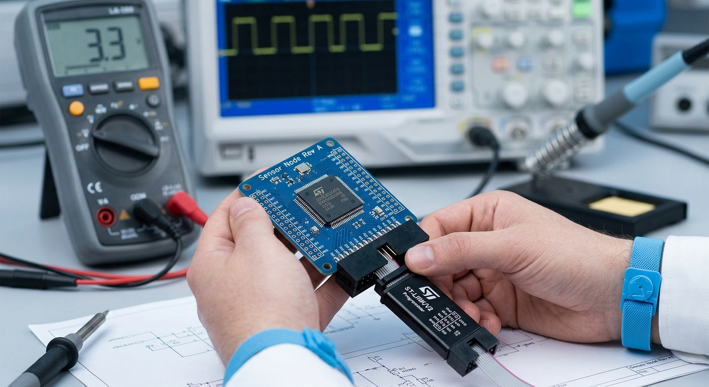
Within these products, the microprocessor can execute application logic while internal flash, eeprom, and memory resources preserve firmware, configuration data, calibration values, and program information. For manufacturers, this embedded information can represent years of engineering investment. However, original source code, development projects, binary, heximal, and engineering archive files may become unavailable as products age.
At the same time, internal storage can be configured as protected, locked, secured, or otherwise encrypted, creating a significant challenge when an organization needs to maintain an existing product. Our “stmicrocontroller stm8l052c6t6 locked flash memory decryption” service is designed to address authorized firmware preservation and engineering recovery requirements involving this type of embedded system.
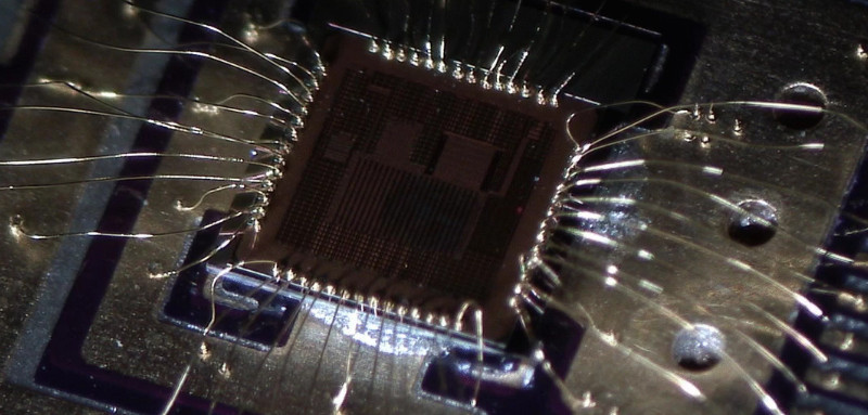
The high-density and medium+ density STM8L15xx6/8x devices feature a nested vectored interrupt controller:
Nested interrupts with 3 software priority levels
32 interrupt vectors with hardware priority
Up to 40 external interrupt sources on 11 vectors
Trap and reset interrupts
The device requires a 1.65 V to 3.6 V operating supply voltage (VDD). The external power supply pins must be connected as follows:
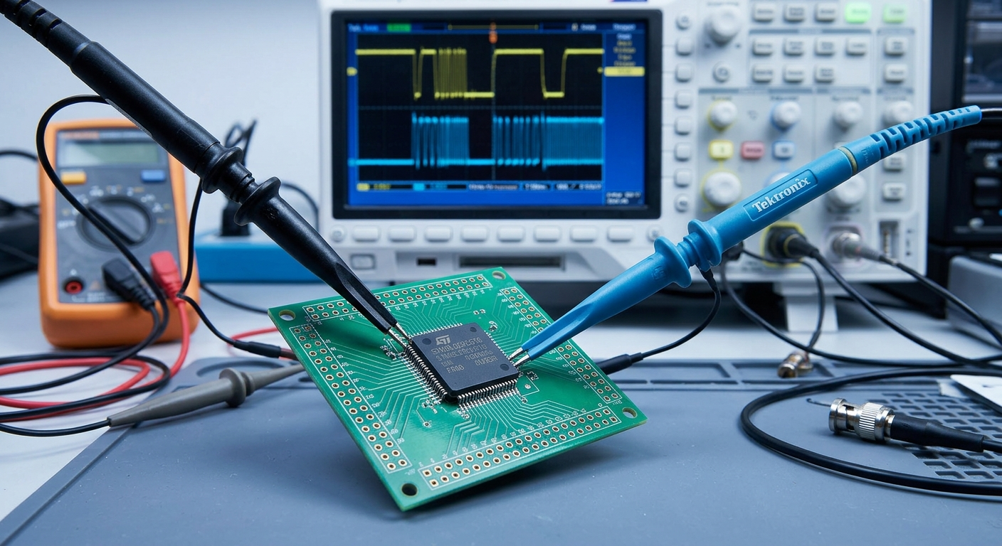
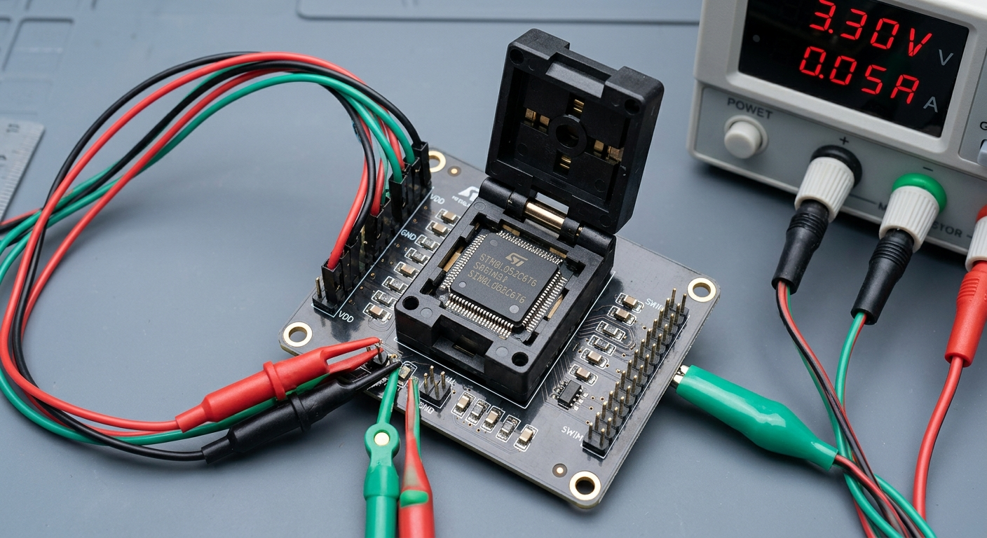
Our service begins with a detailed assessment of the target stm8l052c6t6, its circuit environment, physical condition, and available engineering documentation. Rather than assuming that every locked device can simply be attacked, breaken, or hacked, our engineers first determine the architecture and establish what information can realistically be recovered. Depending on the device and project requirements, controlled semiconductor investigation may be considered, including specialized decapsulate analysis where appropriate and authorized. Available flash, eeprom, and memory information can then be evaluated to determine whether useful firmware, binary, heximal, or configuration data remains accessible. Advanced analysis can retrieve relevant information and decode it into organized file and archive resources for engineering evaluation.
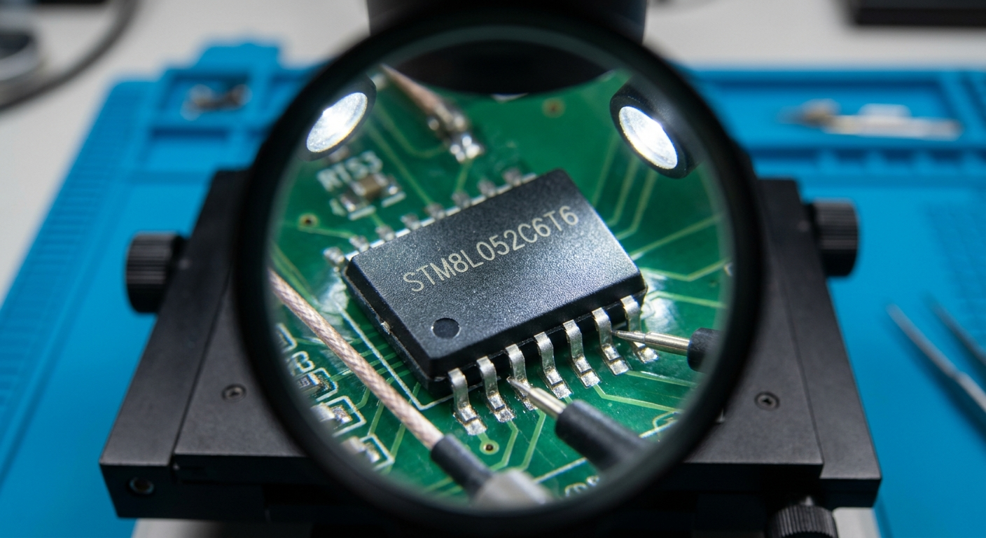
When the customer describes the requirement as locked flash memory decryption, the practical objective is to recover and interpret customer-owned embedded resources rather than provide unauthorized access techniques. Where technically feasible, recovered program information may support controlled clone evaluation, duplicate development, compatibility verification, product repair, or reconstruction of missing documentation. Each protected, locked, or secured device is assessed individually because recovery feasibility depends on the semiconductor architecture and implemented protection mechanism.
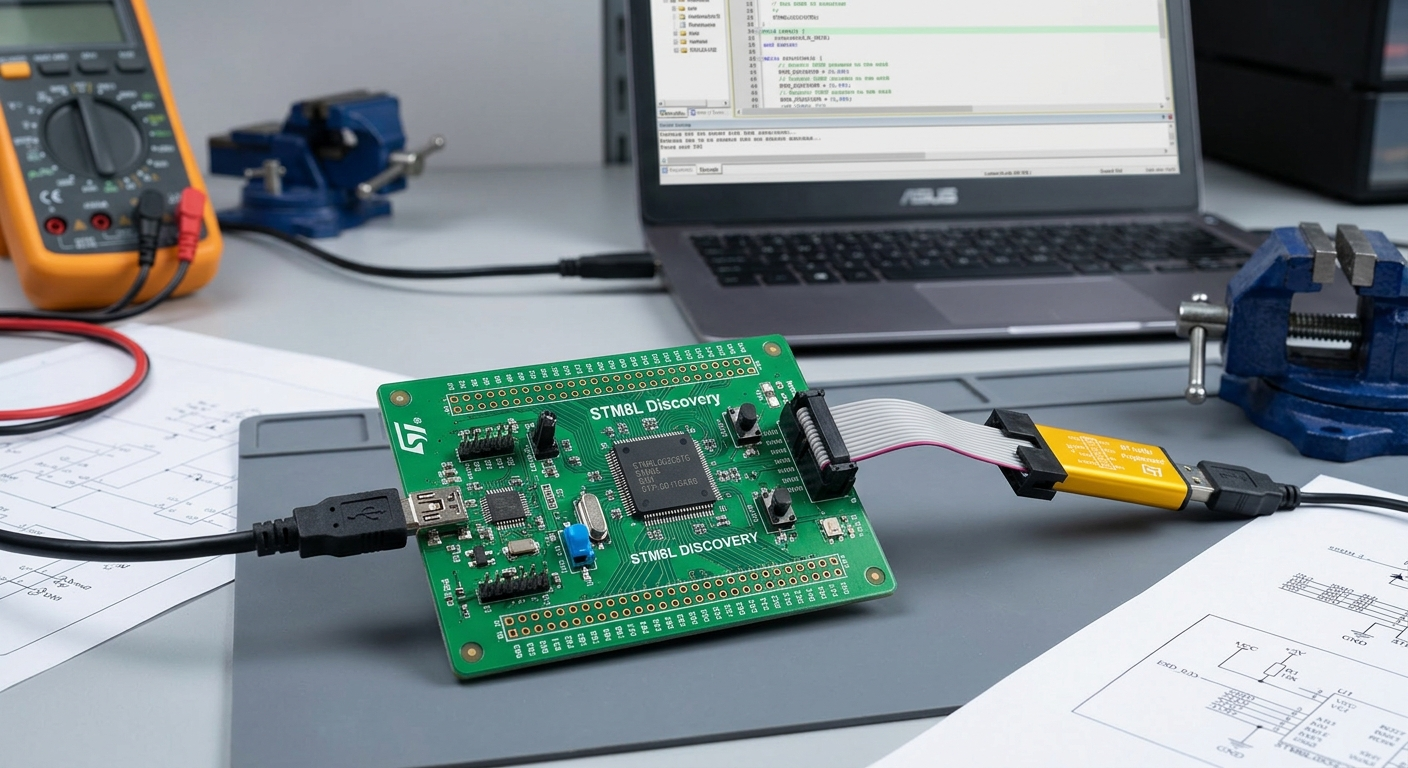
The engineering value of this process extends beyond obtaining a raw memory image. Compiled firmware normally consists of machine-level binary information rather than the developer’s original source code, so professional analysis is required to interpret its functional structure. Engineers can correlate recovered data with PCB connections, peripheral behavior, communication interfaces, timing characteristics, and other system functions to build a more complete understanding of the original product.
Where suitable, laboratory-level decapsulate investigation can complement conventional firmware analysis and help clarify inaccessible internal structures. The resulting technical package may include validated firmware information, organized binary or heximal files, memory observations, program documentation, and engineering archive records. This approach is particularly valuable when an obsolete product must remain operational but its original development environment, programmer configuration, or source files have disappeared.
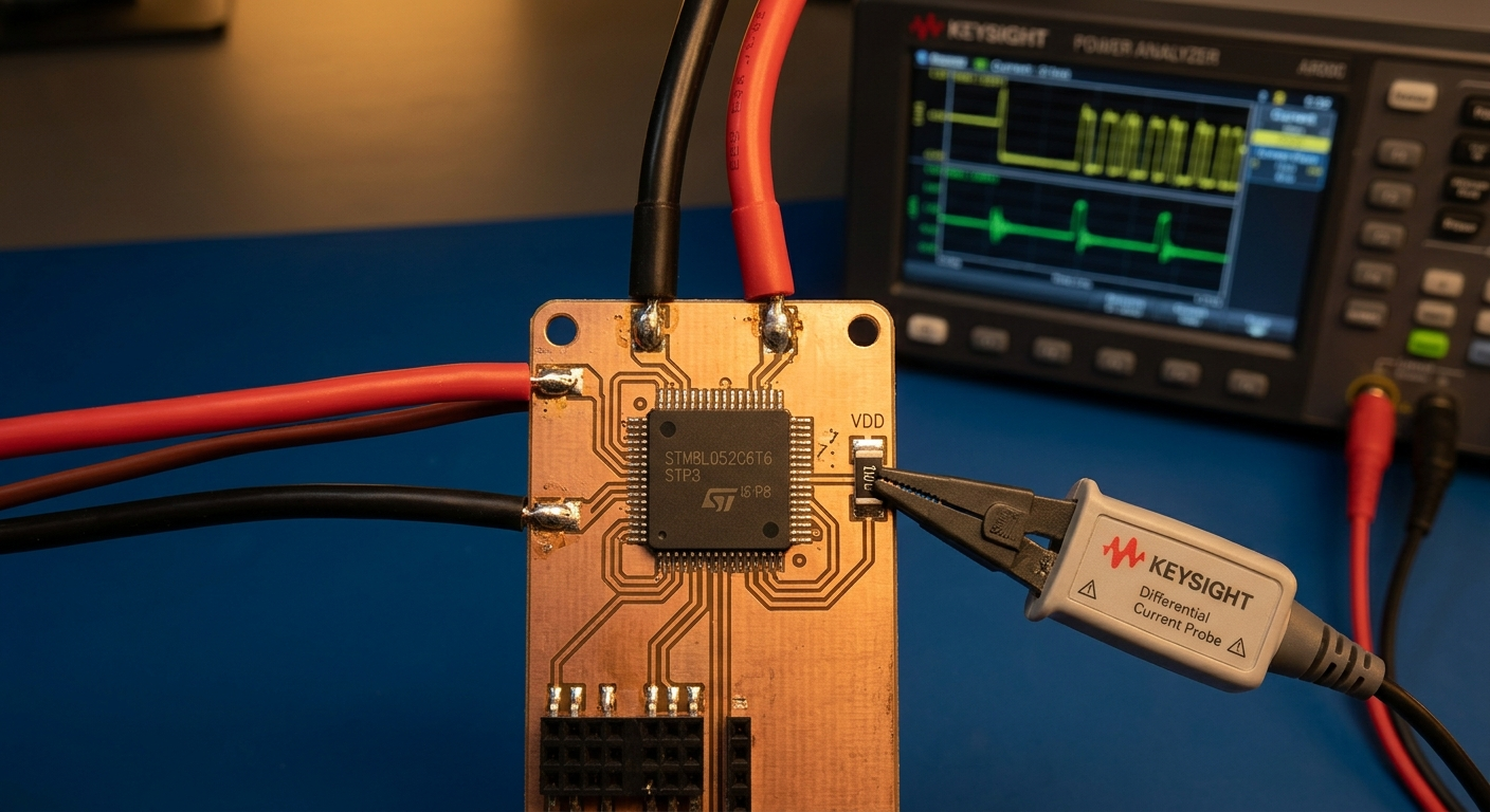
For equipment manufacturers, maintenance organizations, and authorized product owners, professional recovery of stm8l052c6t6 flash information can reduce redevelopment costs and extend the service life of established products. Recovered firmware, program, and data resources can assist with troubleshooting, replacement-board development, product migration, documentation reconstruction, and future modernization.
Instead of recreating a mature embedded system entirely from the beginning, engineering teams can use information recovered from an existing mcu as a technical reference for continued development. Our service combines embedded-system expertise, stmicro device analysis, memory investigation, and firmware reconstruction to help customers preserve valuable engineering knowledge contained within existing hardware and maintain continuity across long-life electronic products.
 Posted in
Duplicate DSP TMS320F28055PNT Microcontroller Binary
The TMS320F28055PNT is a digital signal controller from Texas Instruments’ C2000 family, designed for embedded systems that require fast real-time processing, accurate control, and integrated peripheral resources. As a DSP-oriented microcontroller, it is particularly suitable for applications where control algorithms, signal processing, feedback monitoring, and precise timing need to operate together within a dedicated electronic system.
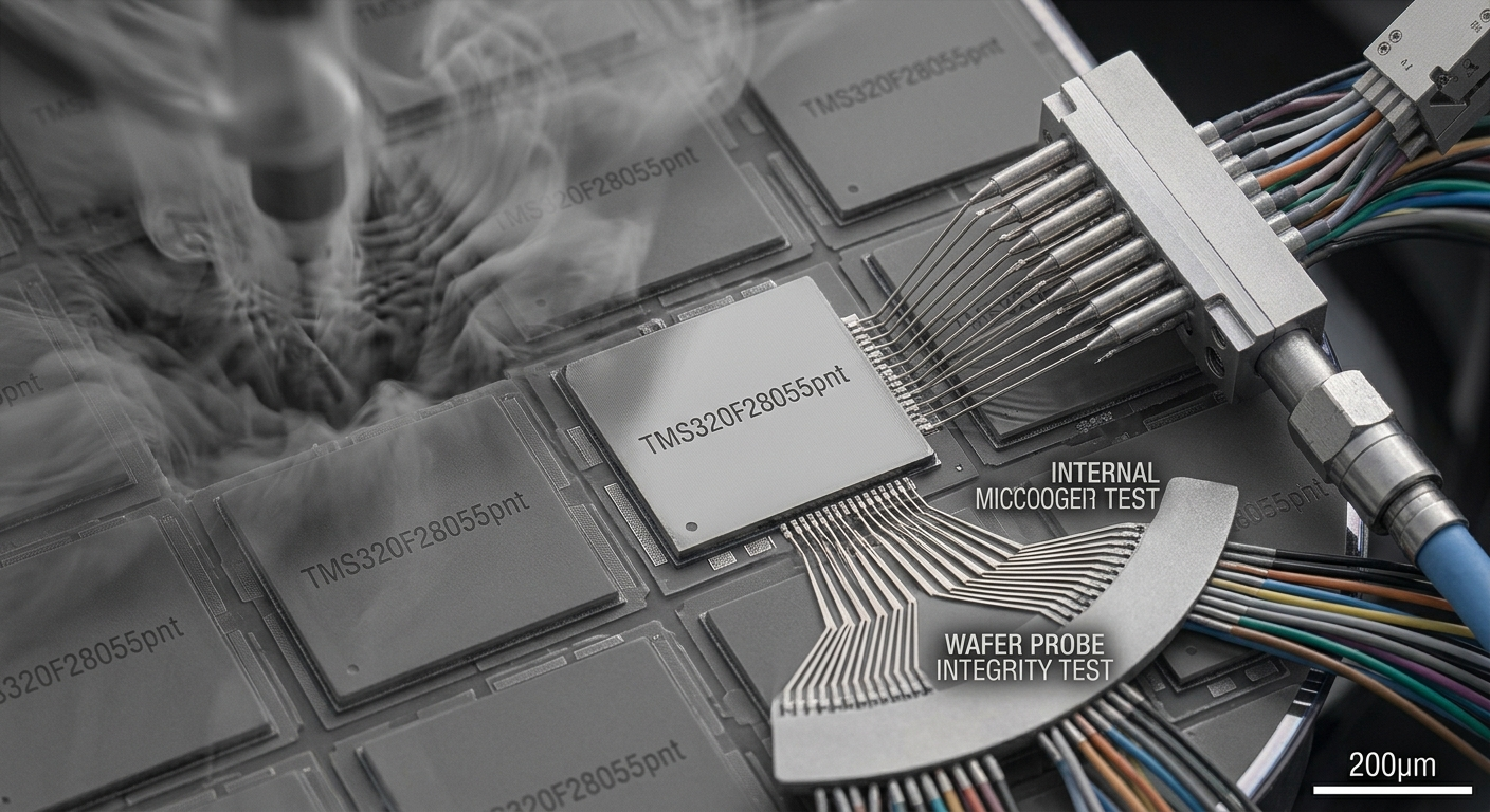
Its capabilities make it applicable to motor drives, industrial automation, digital power supplies, solar and renewable-energy equipment, inverters, power conversion systems, energy-management equipment, and other industrial control platforms. In these applications, the programmed controller can contain essential operating logic that determines how the equipment responds to sensors, power stages, motors, communications, and other hardware, making preservation of its binary information important when maintaining established products.
To designate the stages in the product development cycle, TI assigns prefixes to the part numbers of all TMS320™ MCU devices and support tools. Each TMS320 MCU commercial family member has one of three prefixes: TMX, TMP, or TMS (for example, TMS320F28069). Texas Instruments recommends two of three possible prefix designators for its support tools: TMDX and TMDS. These prefixes represent evolutionary stages of product development from engineering prototypes (with TMX for devices and TMDX for tools) to fully qualified production devices/tools (with TMS for devices and TMDS for tools).

Device development evolutionary flow:
When an electronic controller has been operating successfully for years, the original development environment may no longer be available even though the programmed TMS320F28055PNT remains functional. Missing source code, firmware projects, engineering documentation, software backups, or archived production files can create difficulties when a controller needs to be repaired or reproduced. A protective, secured, encrypted, or locked device can add another layer of difficulty by preventing conventional access to its internal program memory. For authorized equipment owners and engineers, recovering the available firmware or binary information can support replacement-board development, discontinued-product maintenance, controller duplication, troubleshooting, functional comparison, and long-term preservation. In particular, an accessible binary image can provide a valuable reference when the objective is to reproduce an existing controller without having to recreate the original embedded application entirely from the beginning.
TMP Final silicon die that conforms to the device’s electrical specifications but has not completed quality and reliability verification
TMS Fully qualified production device Support tool development evolutionary flow:
For a TMS32F28055PNT binary recovery project, engineers can first inspect the target hardware, identify the processor and its programming or debugging interfaces, and evaluate its memory organization and protection configuration. Depending on the device condition and authorized objective, technical methods can be investigated to determine whether firmware, source code, data, software, memory, archive, flash, or eeprom information can be retrieved, decoded, duplicated, or cloned.

If a protective, secured, encrypted, or locked configuration restricts normal readout, specialists may evaluate appropriate approaches to break or attack the relevant access restriction. Where conventional interface methods cannot provide sufficient information, advanced semiconductor analysis may include controlled decapsulation of the microcontroller, microprocessor, MCU, chip, or IC. The practical result depends on the specific protection condition, physical state, memory contents, available interfaces, and recovery requirements of the target TMS32F28055PNT; therefore, the feasibility of producing a usable binary from another TMS32F28055PNT must be assessed individually, while any work involving a third TMS32F28055PNT should likewise be based on its actual device condition rather than a universal recovery assumption.

Our TMS320F28055PNT binary duplication and firmware recovery service helps authorized manufacturers, equipment owners, repair companies, and engineering teams preserve important embedded software from existing control systems. We can examine the target board, identify the installed DSP controller, investigate available programming and debugging paths, and evaluate memory and protection conditions before selecting a suitable recovery strategy.

Where technically feasible, our service can assist with obtaining recoverable firmware or binary information and preparing it for authorized replacement-controller programming, product restoration, redesign, engineering analysis, or maintenance. This is particularly useful when the original source-code archive has disappeared but a working or partially functional controller remains available. By combining device identification, hardware investigation, memory analysis, firmware examination, and specialized recovery techniques, we help customers preserve valuable binary information and support the continued operation or reproduction of established electronic control equipment.

Decode ST CPU ST72F321R9 Processor Locked Memory File
Decode ST CPU ST72F321R9 Processor Locked Memory File needs to use laser cutting to remove the security fuse bit of microcontroller, and then copy embedded flash firmware from mcu st72f321r9;
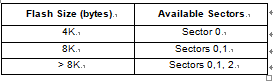
The Flash memory is organised in sectors and can be used for both code and data storage.
Depending on the overall Flash memory size in the micro-controller device, there are up to three user sectors (see below Table). Each of these sectors can be erased independently to avoid unnecessary erasing of the whole Flash memory when only a partial erasing is required after breaking st72f32ak1 mcu flash memory protection.
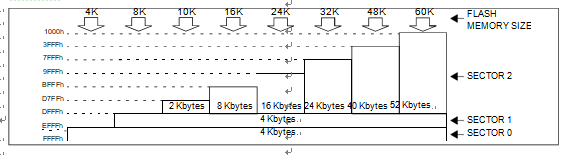
The first two sectors have a fixed size of 4 Kbytes (see below Figure). They are mapped in the upper part of the ST7 addressing space so the reset and in- terrupt vectors are located in Sector 0 (F000h- FFFFh).
3.5.1 Power supply schemes
- VDD = 2.4 to 3.6 V: external power supply for I/Os and the internal regulator. Provided externally through VDD pins.
- VDDA = from VDD to 3.6 V: external analog power supply for ADC, Reset blocks, RCs and PLL. The VDDA voltage level must be always greater or equal to the VDD voltage level and must be provided first.
Decrypt ST72F321BK MCU Flash Memory Program
Decrypt ST72F321BK MCU Flash Memory Program is a process to pull the embedded firmware from st72f321bk mcu flash memory and then copy the heximal to new microcontroller;
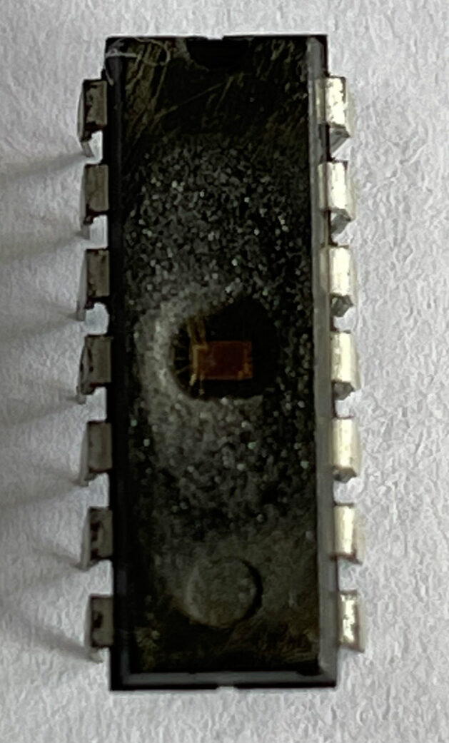
The ST7 dual voltage High Density Flash (HDFlash) is a non-volatile memory that can be electrically erased as a single block or by individu- al sectors and programmed on a Byte-by-Byte ba- sis using an external VPP supply.
The HDFlash devices can be programmed and erased off-board (plugged in a programming tool) or on-board using ICP (In-Circuit Programming) or IAP (In-Application Programming) which can be applied for breaking mcu st72f321j9 flash memory.
The array matrix organisation allows each sector to be erased and reprogrammed without affecting other sectors.
- Three Flash programming modes:
- Insertion in a programming tool. In this mode, all sectors including option bytes can be pro- grammed or erased.
- ICP (In-Circuit Programming). In this mode, all sectors including option bytes can be pro- grammed or erased without removing the de- vice from the application board.
- IAP (In-Application Programming) In this mode, all sectors except Sector 0, can be pro- grammed or erased without removing the de- vice from the application board and while the application is running.
- ICT (In-Circuit Testing) for downloading and executing user application test patterns in RAM when attacking st72f321ar mcu protected flash memory
- Read-out protection
- Register Access Security System (RASS) to prevent accidental programming or erasing
Attack STMicro ST72F321AR IC Chip Secured Memory
Attack STMicro ST72F321AR IC Chip Secured Memory and extract embedded MCU heximal file from flash memory, the firmware can be rewrite to new microprocessor st72f321ar for cloning;
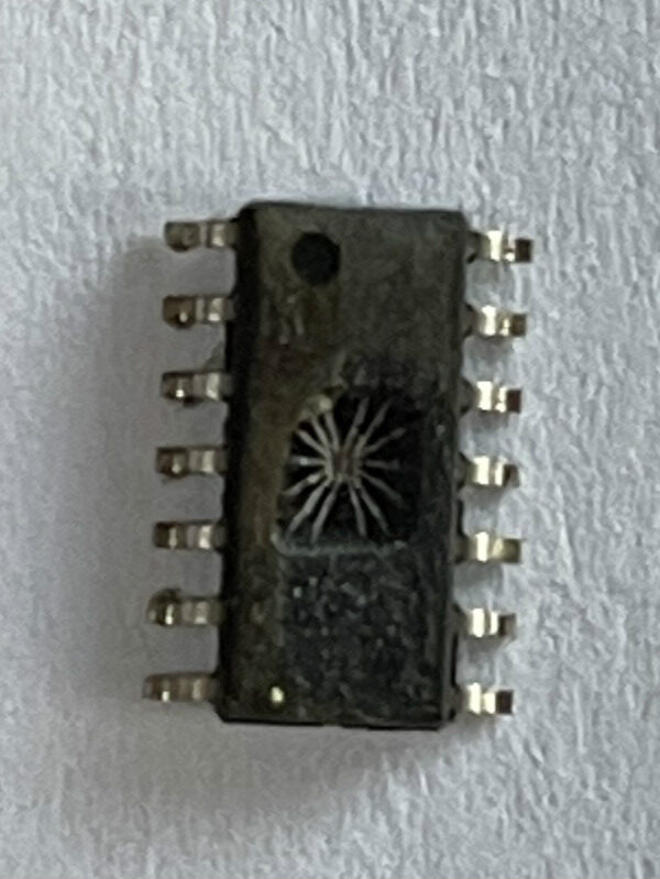
the MCU is capable of ad- dressing 64K bytes of memories and I/O registers.
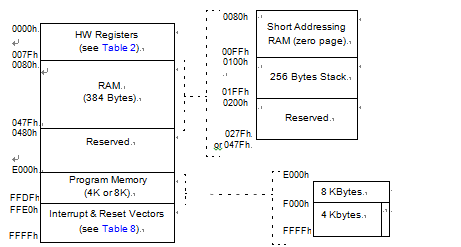
The available memory locations consist of 128 bytes of register locations, up to 384 bytes of RAM and up to 8 Kbytes of user program memory. The RAM space includes up to 256 bytes for the stack from 0100h to 01FFh by reversing microcontroller st72f32aj1 microcontroller flash memory binary.
The highest address bytes contain the user reset and interrupt vectors.
IMPORTANT: Memory locations marked as “Re- served” must never be accessed. Accessing a re- served area can have unpredictable effects on the devices.
The contents of the I/O port DR registers are readable only in output configuration. In input configuration, the values of the I/O pins are returned instead of the DR register contents after breaking st72f321aj mcu flash memory fuse bit.
The bits associated with unavailable pins must always keep their reset value.
Break ST72F321J9 Microcontroller Flash/ROM Memory
Break ST72F321J9 Microcontroller Flash/ROM Memory and extract embedded data from secured flash controlled by microprocessor ST72F321J9, and then crack secured mcu st72f321j9 security fuse bit;
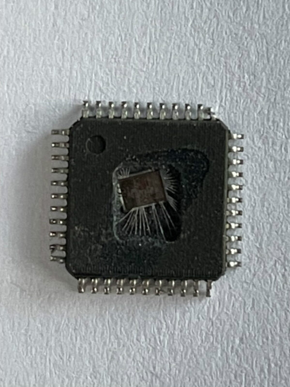
PIN DESCRIPTION (Cont’d)
For external pin connection guidelines, refer to See “ELECTRICAL CHARACTERISTICS” on page 113.
Legend / Abbreviations for Table 1:
Type: I = input, O = output, S = supply
Input level: A = Dedicated analog input In/Output level: C = CMOS 0.3VDD/0.7VDD
CT= CMOS 0.3VDD/0.7VDD with input trigger Output level:
HS = 20mA high sink (on N-buffer only)
Port and control configuration:
- Input:
- float = floating, wpu = weak pull-up, int = interrupt 1), ana = analog ports
- Output: OD = open drain 2), PP = push-pull
Refer to “I/O PORTS” on page 42 for more details on the software configuration of the I/O ports.
The RESET configuration of each pin is shown in bold. This configuration is valid as long as the device is in reset state.
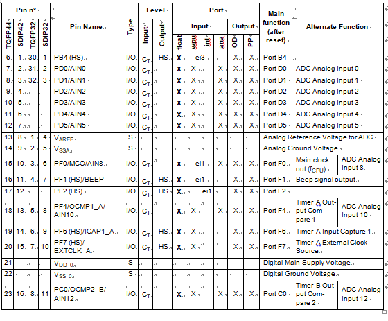
- In the interrupt input column, “eiX” defines the associated external interrupt vector. If the weak pull-up column (wpu) is merged with the interrupt column (int) when breaking st72f32ak1 microcontroller flash memory, then the I/O configuration is pull-up interrupt input, else the configuration is floating interrupt input.
- In the open drain output column, “T” defines a true open drain I/O (P-Buffer and protection diode to VDD are not implemented). See See “I/O PORTS” on page 42. and Section 12.8 I/O PORT PIN CHARACTER- ISTICS for more details.
- OSC1 and OSC2 pins connect a crystal/ceramic resonator, or an external source to the on-chip oscil- lator; see Section 1 INTRODUCTION and Section 12.5 CLOCK AND TIMING CHARACTERISTICS for more details.
- On the chip, each I/O port has 8 pads. Pads that are not bonded to external pins are in input pull-up configuration after reset and restore st72f32ak2 mcu encrypted flash heximal. The configuration of these pads must be kept at reset state to avoid added current consumption.
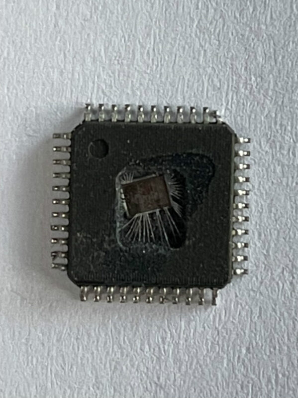
Break STMicrocontroller ST72F32AK1 Flash Memory Protection
Break STMicrocontroller ST72F32AK1 Flash Memory Protection needs to remove the fuse bit of mcu embedded system and readout the locked memory firmware from processor;
8K dual voltage High Density Flash (HDFlash) or ROM with read-out protection capability. In- Application Programming and In-Circuit Pro- gramming for HDFlash devices
384 bytes RAM
HDFlash endurance: 100 cycles, data reten- tion: 40 years at 85°C
■ Clock, Reset And Supply Management
Clock sources: crystal/ceramic resonator os- cillators and bypass for external clock
PLL for 2x frequency multiplication
Four Power Saving Modes: Halt, Active-Halt, Wait and Slow
■ Interrupt Management
Nested interrupt controller
14 interrupt vectors plus TRAP and RESET
6 external interrupt lines (on 4 vectors)
■ Up to 32 I/O Ports
32/24 multifunctional bidirectional I/O lines
22/17 alternate function lines
12/10 high sink outputs
■ 4Timers
Main Clock Controller with: Real time base, Beep and Clock-out capabilities
Configurable watchdog timer in order to break stm8s207k6 locked mcu memory
Two 16-bit Timers with: 2 input captures, 2 output compares, PWM and pulse generator modes
■ 2 Communications Interfaces
SPI synchronous serial interface
SCI asynchronous serial interface
– 10-bit ADC with up to 12 robust input ports
■ Instruction Set
8-bit Data Manipulation
63 Basic Instructions when recover secured stm8s207c6 microcontroller heximal file
17 main Addressing Modes
8 x 8 Unsigned Multiply Instruction
■ Development Tools
Full hardware/software development package
In-Circuit Testing capability
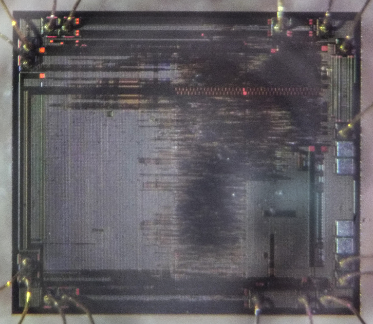
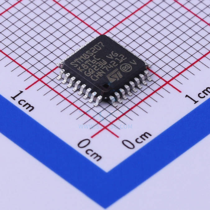
Secured Microcontroller STM8S207K8T6 Flash Heximal Code Unlocking
Secured Microcontroller STM8S207K8T6 Flash Heximal Code Unlocking will be able to reset the MCU status and readout software from stm8s207k8 program flash memory directly, the fuse bit of processor’s stm8s207k8 will be cracked by focus ion beam;
Susceptibility tests are performed on a sample basis during product characterization.
Functional EMS (electromagnetic susceptibility)
While executing a simple application (toggling 2 LEDs through I/O ports), the product is stressed by two electromagnetic events until a failure occurs (indicated by the LEDs).
ESD: Electrostatic discharge (positive and negative) is applied on all pins of the device until a functional disturbance occurs. This test conforms with the IEC 61000-4-2 standard.
güvenli mikrodenetleyici STM8S207K8T6 flaş onaltılık kod kilidini açma, MCU durumunu sıfırlayabilecek ve yazılımı doğrudan stm8s207k8 program flash belleğinden okuyabilecek, işlemcinin stm8s207k8’inin sigorta biti odak iyon ışını ile kırılacaktır;
FTB: A burst of fast transient voltage (positive and negative) is applied to VDD and VSS through a 100 pF capacitor, until a functional disturbance occurs. This test conforms with the IEC 61000-4-4 standard which is an important fact for reversing stm8s005 mcu flash memory code.
A device reset allows normal operations to be resumed. The test results are given in the table below based on the EMS levels and classes defined in application note AN1709 (EMC design guide for STM microcontrollers).
Designing hardened software to avoid noise problems
EMC characterization and optimization are performed at component level with a typical application environment and simplified MCU software. It should be noted that good EMC performance is highly dependent on the user application and the software in particular by recovering stm8s005k6 microcontroller data eeprom content.
Therefore it is recommended that the user applies EMC software optimization and prequalification tests in relation with the EMC level requested for his application.
ST STM8S207K6 Locked Microcontroller Memory Breaking
ST STM8S207K6 Locked Microcontroller Memory Breaking is a process to reverse engineering stm8s207k6 microcontroller structure and disable its protection and reset the status from locked to unlocked, copy embedded firmware from stm8s207k6 mcu flash content;
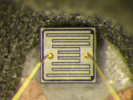
Write protection of Flash program memory and data EEPROM is provided to avoid unintentional overwriting of memory that could result from a user software malfunction.
There are two levels of write protection. The first level is known as MASS (memory access security system). MASS is always enabled and protects the main Flash program memory, data EEPROM and option bytes and we have to use technique to reverse mcu stm8s005c6 flash memory code.
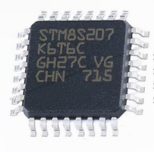
ST STM8S207K6 gesperrter Mikrocontroller-Speicherbruch ist ein Prozess zum Reverse Engineering von STM8S207K6-Mikrocontrollern
Strukturieren und deaktivieren Sie den Schutz und setzen Sie den Status von gesperrt auf entsperrt zurück, kopieren Sie die eingebettete Firmware aus dem MCU-Flash-Inhalt STM8S207K6
To perform in-application programming (IAP), this write protection can be removed by writing a MASS key sequence in a control register. This allows the application to write to data EEPROM, modify the contents of main program memory or the device option bytes.
A second level of write protection, can be enabled to further protect a specific area of memory known as UBC (user boot code).
The size of the UBC is programmable through the UBC option byte, in increments of 1 page (512 bytes) by programming the UBC option byte in ICP mode when break mcu stm8s103f3 flash memory.
This divides the program memory into two areas:
Main program memory: Up to 128 Kbytes minus UBC
User-specific boot code (UBC): Configurable up to 128 Kbytes
The UBC area remains write-protected during in-application programming. This means that the MASS keys do not unlock the UBC area. It protects the memory used to store the boot program, specific code libraries, reset and interrupt vectors, the reset routine and usually the IAP and communication routines.
Hack STM8S105C6T3 Microprocessor Flash and Eeprom Memory
Hack STM8S105C6T3 Microprocessor Flash and Eeprom Memory needs to crack stm8s105 mcu protective system including remove its security fuse bit and then copy locked program from flash and eeprom memory of microcontroller;
Write protection of Flash program memory and data EEPROM is provided to avoid unintentional overwriting of memory that could result from a user software malfunction.
There are two levels of write protection. The first level is known as MASS (memory access security system) when reverse engineering stm8s105k6 data eeprom and program flash system. MASS is always enabled and protects the main Flash program memory, data EEPROM and option bytes.
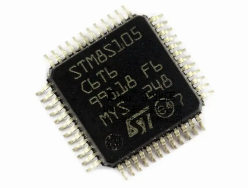
pirater le flash du microprocesseur STM8S105C6T3 et la mémoire eeprom doit craquer le système de protection stm8s105 mcu, y compris retirer son bit de fusible de sécurité, puis copier le programme verrouillé à partir de la mémoire flash et eeprom du microcontrôleur ;
To perform in-application programming (IAP), this write protection can be removed by writing a MASS key sequence in a control register. This allows the application to write to data EEPROM, modify the contents of main program memory or the device option bytes to break mcu stm8s105k4 protective flash and eeprom memory.
A second level of write protection, can be enabled to further protect a specific area of memory known as UBC (user boot code). Refer to the figure below. The size of the UBC is programmable through the UBC option byte, in increments of 1 page (64-byte block) by programming the UBC option byte in ICP mode.